Research on an On-Chip MEMS Based Safety and Arming Device with a Mechanical Encryption System

Abstract
:1. Introduction
2. System Composition
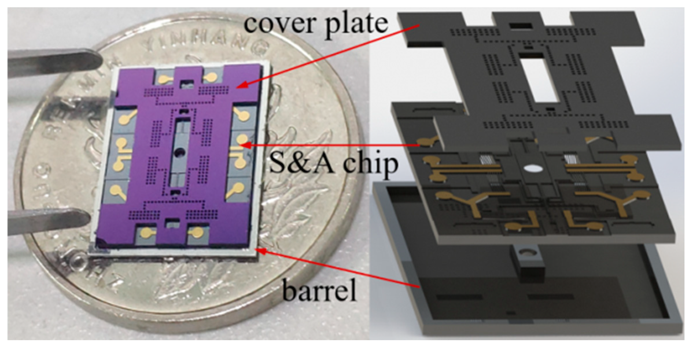
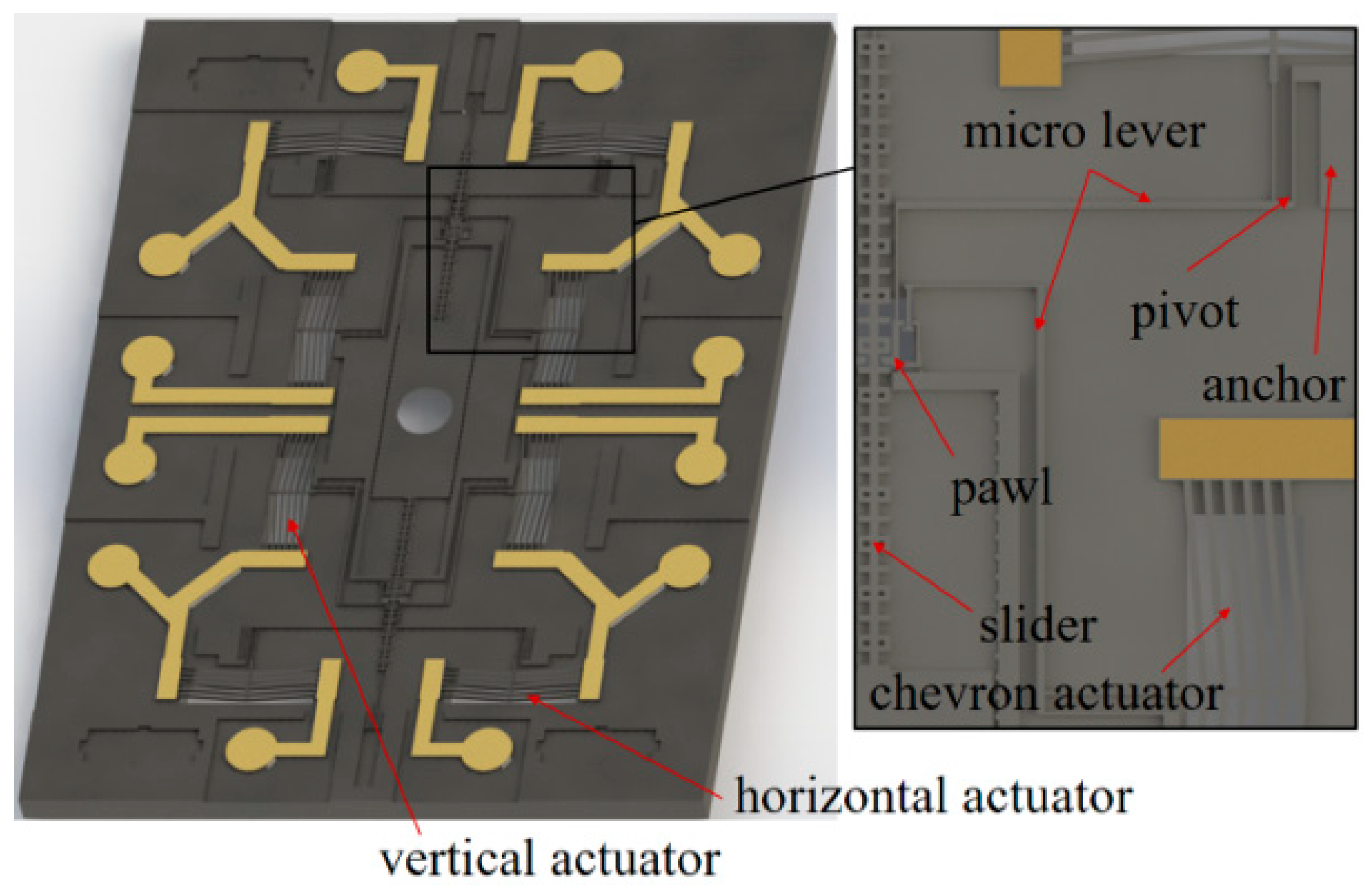
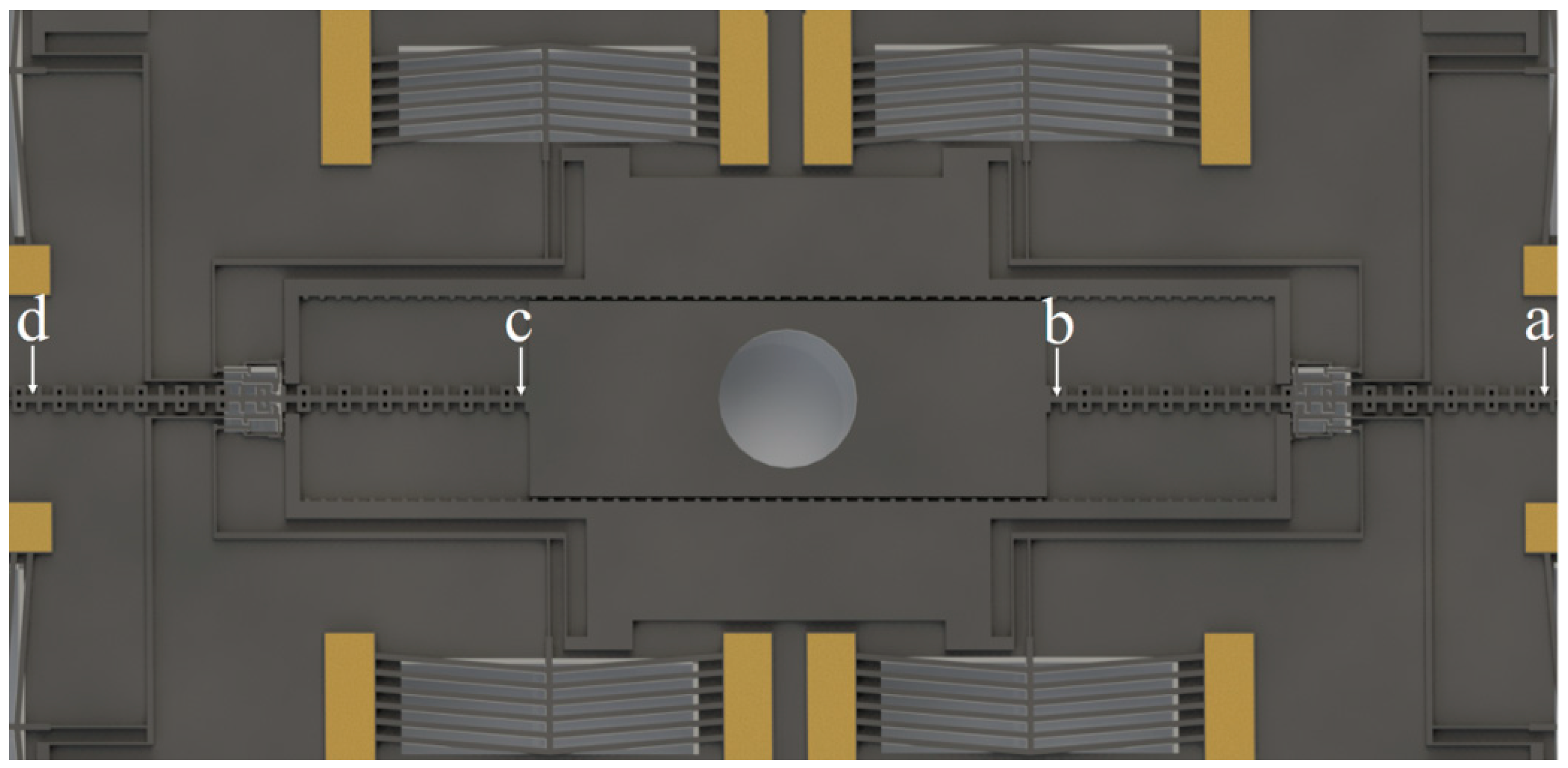
2.1. Device Description
2.2. Working Principle
3. Theoretical Analysis
4. Test and Discussion
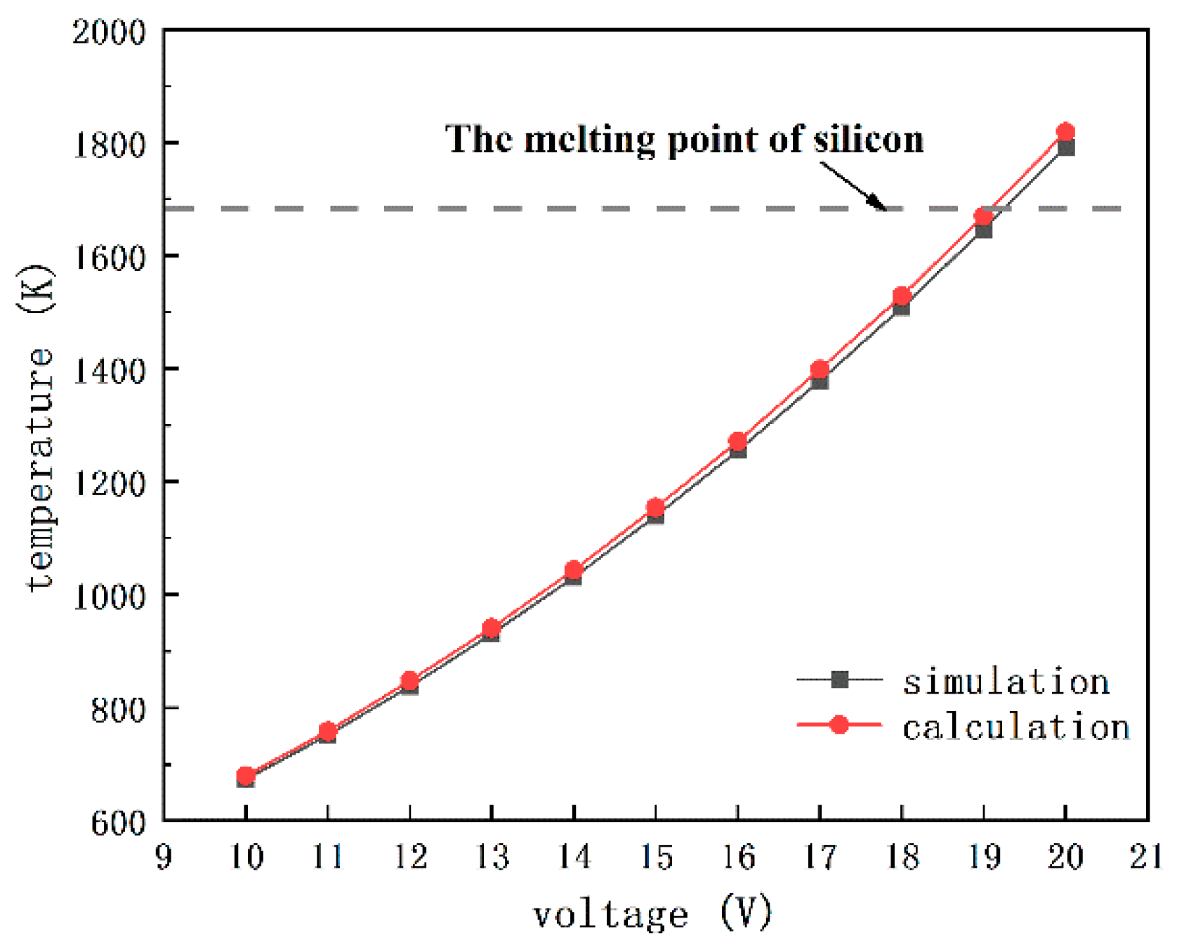
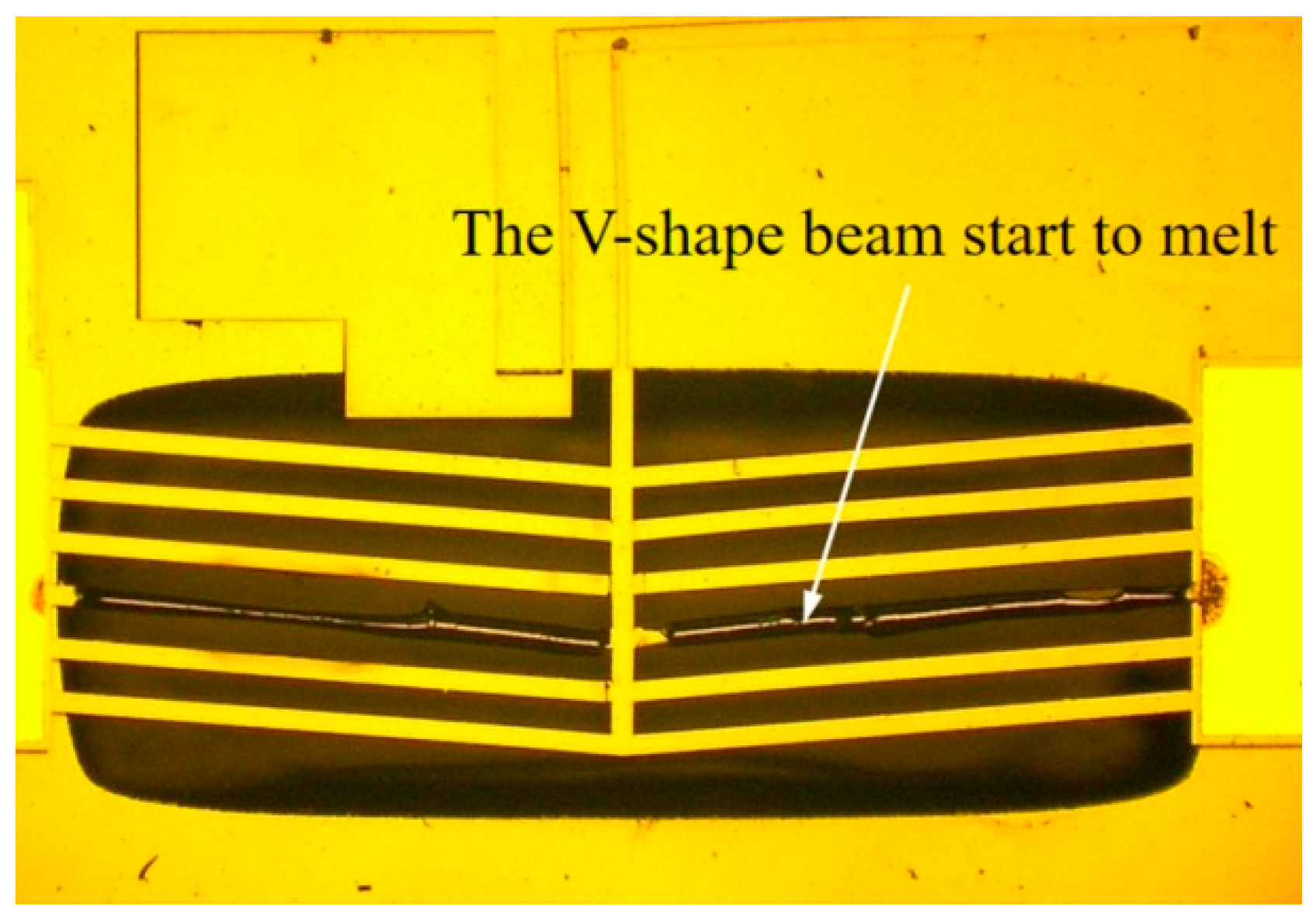
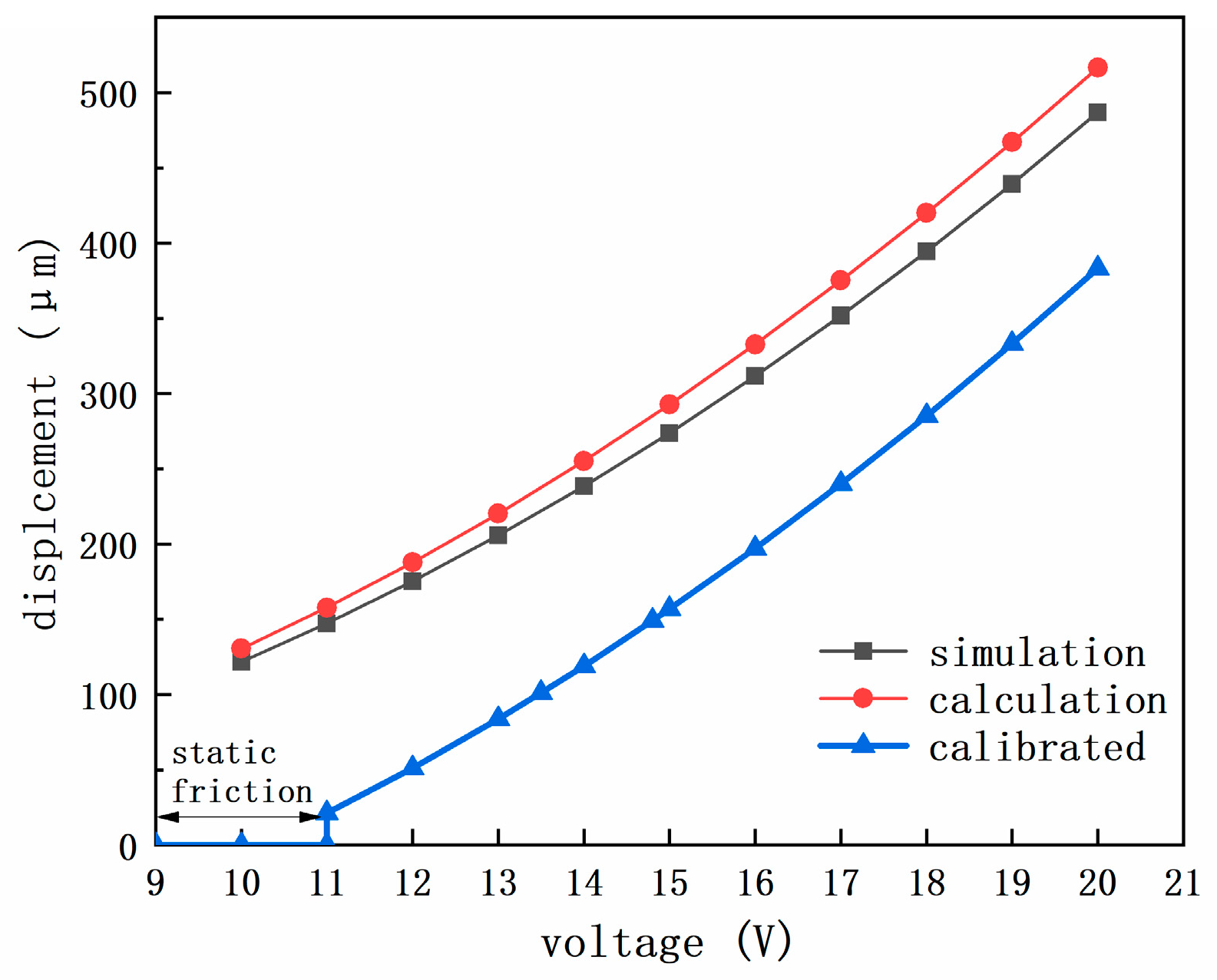
4.1. The Maximum Working Voltage
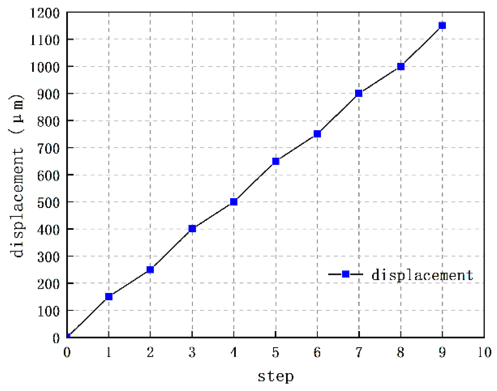
4.2. Moving Test
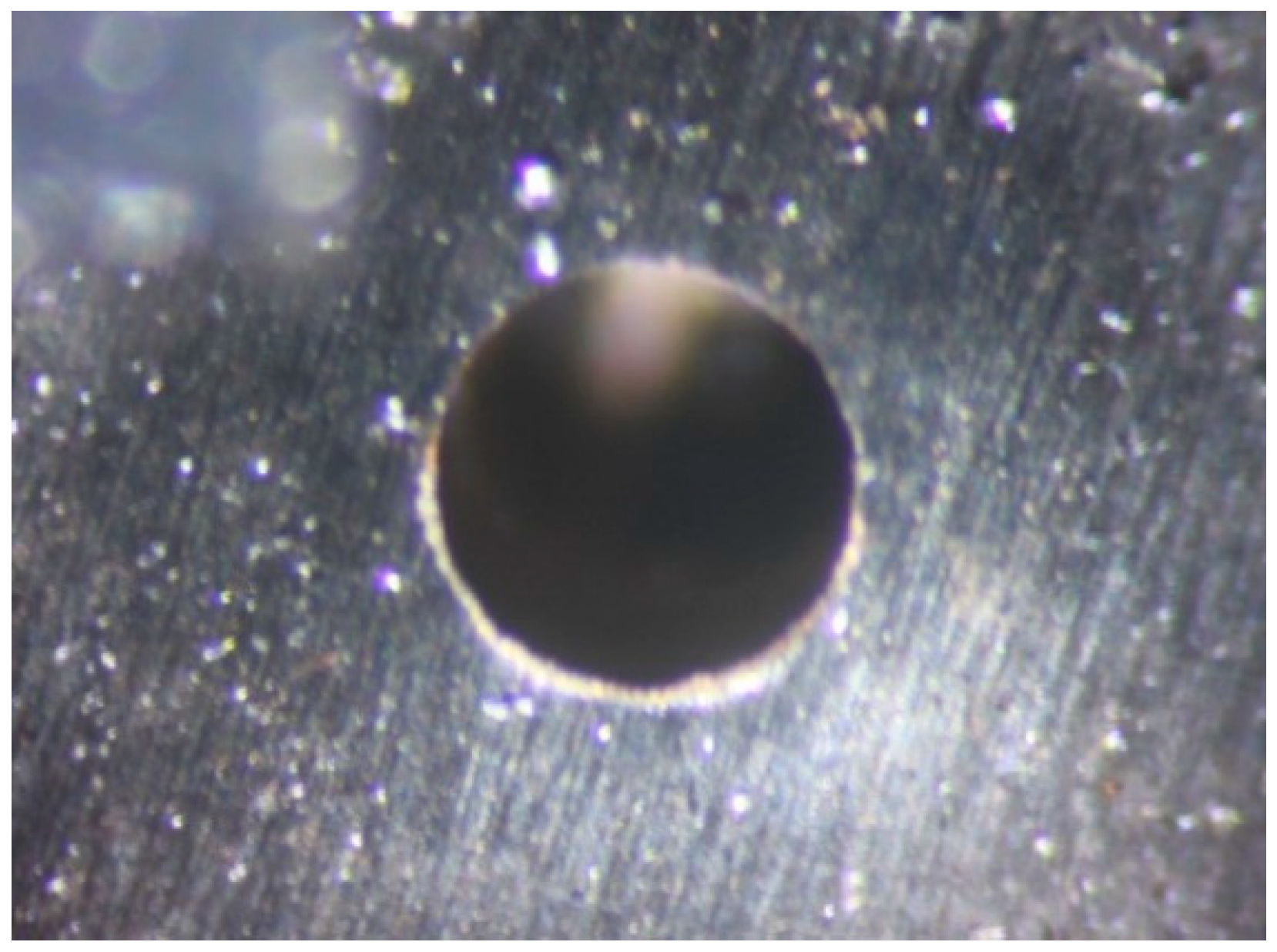
4.3. Firing Test
5. Conclusions and Perspective
- (a)
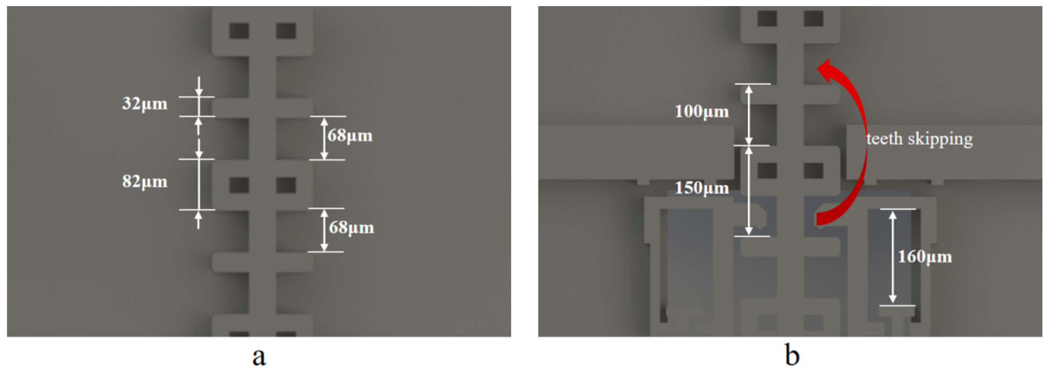
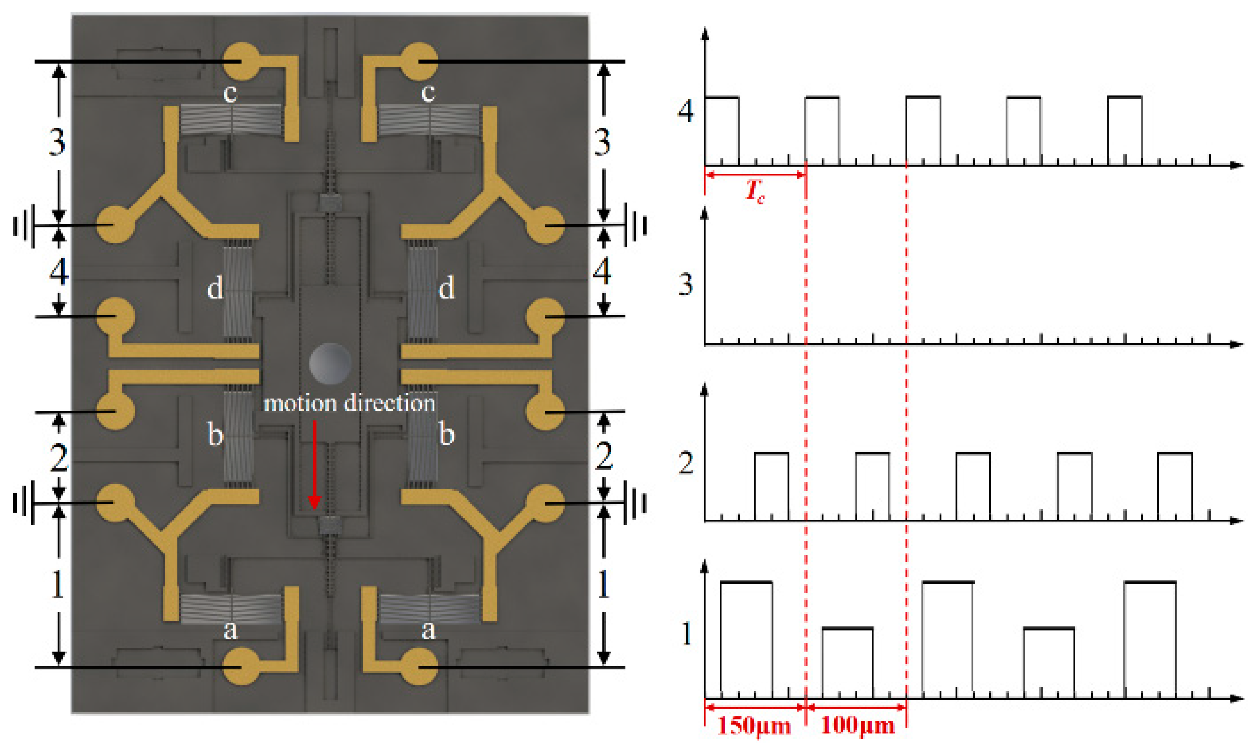
- The amplitude and the timing sequence recognition of input voltages have been achieved through the meshing between the pawl and the teeth on the slider with different width.
- (b)
- The bidirectional actuation design makes the conversion between safe status and arm status reversible. The travel range of interrupter in the SAD will only be limited by the chip dimension due to the feature of motion retention, which indicates that the design method is able to cover a wide range of microfuze with different requirement on the travel range of interrupter.
- (c)
- The relationship between the input voltage and output of the pawl has been analyzed. Based on our design method, the prototype of encryption system can evolve into numerous kinds of variants for application in the microfuze.
- (d)
- According to the firing test, after a flight of about 753 μm in the SAD, the titanium flyer is still able to reach an average velocity about Vavg = 1873.3 m/s, which indicates that there is not any obvious negative effect on flyer acceleration that is caused by the integration of the SAD on the explosive train.
- (e)
- For the dynamic performance optimization, the microtribology on the interface between the slider and the substrate is worthwhile to investigate in future work.
Author Contributions
Funding
Acknowledgments
Conflicts of Interest
References
- Seok, J.O.; Jeong, J.H.; Eom, J.; Lee, S.S.; Lee, C.J.; Ryu, S.M.; Oh, J.S. Ball driven type MEMS SAD for artillery fuse. J. Micromech. Microeng. 2017, 27, 015032. [Google Scholar] [CrossRef]
- Pezous, H.; Rossi, C.; Sanchez, M.; Mathieu, F.; Dollat, X.; Charlot, S.; Salvagnac, L.; Conédéra, V. Integration of a MEMS based safe arm and fire device. Sens. Actuators A Phys. 2010, 159, 157–167. [Google Scholar] [CrossRef]
- Mukhopadhyay, D.; Dong, J.; Pengwang, E.; Ferreira, P. A SOI-MEMS-based 3-DOF planar parallel-kinematics nanopositioning stage. Sens. Actuators A Phys. 2008, 147, 340–351. [Google Scholar] [CrossRef]
- Kim, Y.S.; Yoo, J.M.; Yang, S.H.; Choi, Y.M.; Dagalakis, N.G.; Gupta, S.K. Design, fabrication and testing of a serial kinematic MEMS XY stage for multifinger manipulation. J. Micromech. Microeng. 2012, 22, 085029. [Google Scholar] [CrossRef]
- Kim, Y.S.; Shi, H.; Dagalakis, N.G.; Gupta, S.K. Design of a MEMS-based motion stagebased on a lever mechanism for generating large displacements and forces. J. Micromech. Microeng. 2016, 26, 095008. [Google Scholar] [CrossRef]
- Sinclair, M.J. A High Force Low Area MEMS Thermal Actuator. In Proceedings of the Seventh Intersociety Conference on Thermal and Thermomechanical Phenomena in Electronic Systems, Las Vegas, NV, USA, 23–26 May 2000; IEEE: Piscataway, NJ, USA, 2000; Volume 1, pp. 127–132. [Google Scholar]
- Reid, J.R.; Bright, V.M.; Comtois, J.H. Force Measurements of Polysilicon Thermal Micro-Actuators. Proc. SPIE Int. Soc. Opt. Eng. 1996, 2882, 296–306. [Google Scholar]
- Cochran, K.R.; Fan, L.; DeVoe, D.L. High-power optical microswitch based on direct fiber actuation. Sens. Actuators A Phys. 2005, 119, 512–519. [Google Scholar] [CrossRef]
- Li, X.; Zhao, Y.; Hu, T.; Xu, W.; Zhao, Y.; Bai, Y.; Ren, W. Design of a large displacement thermal actuator with a cascaded V-beam amplification for MEMS safety-and-arming devices. Microsyst. Technol. 2015, 21, 2367–2374. [Google Scholar] [CrossRef]
- Ostrow, S.A., II; Lake, R.A.; Lombardi, J.P., III; Coutu, R.A.; Starman, L.A. Fabrication Process Comparison and Dynamics Evaluation of Electrothermal Actuators for a Prototype MEMS Safe and Arming Devices. Exp. Mech. 2012, 52, 1229–1238. [Google Scholar] [CrossRef]
- Hu, T.; Fang, K.; Zhang, Z.; Jiang, X.; Zhao, Y. Design and research on large displacement bidirectional MEMS stage with interlock mechanism. Sens. Actuators A Phys. 2018, 283, 26–33. [Google Scholar] [CrossRef]
- Zhang, Y.; Huang, Q.A.; Li, R.G.; Li, W. Macro-modeling for polysilicon cascaded bent beam electrothermal microactuators. Sens. Actuators A Phys. 2006, 128, 165–175. [Google Scholar] [CrossRef]
- Yang, Y.S.; Lin, Y.H.; Hu, Y.C.; Liu, C.H. A large-displacement thermal actuator designed for MEMS pitch-tunable grating. J. Micromech. Microeng. 2009, 19, 015001. [Google Scholar] [CrossRef]
- Kolesar, E.S.; Ko, S.Y.; Howard, J.T.; Allen, P.B.; Wilken, J.M.; Boydston, N.C.; Ruff, M.D.; Wilks, R.J. In-plane tip deflection and force achieved with asymmetrical polysilicon electrothermal microactuators. Thin Solid Films 2000, 377, 719–726. [Google Scholar] [CrossRef]
- Su, X.P.S.; Yang, H.S. Design of compliant microleverage mechanisms. Sens. Actuators A Phys. 2001, 87, 146–156. [Google Scholar] [CrossRef]
- Su, X.P.; Yang, H.S. Single-stage microleverage mechanism optimization in a resonant accelerometer. Struct. Multidiscip. Optim. 2001, 21, 246–252. [Google Scholar] [CrossRef]
- Huang, Q.A.; Lee, N.K.S. Analysis and design of polysilicon thermal flexure actuator. J. Micromech. Microeng. 1999, 9, 64–70. [Google Scholar] [CrossRef]
- Lott, C.D.; McLain, T.W.; Harb, J.N.; Howell, L.L. Howell. Modeling of the thermal behavior of a surface-micromachined linear-displacement thermomechanical microactuator. Sens. Actuators A Phys. 2002, 101, 239–250. [Google Scholar] [CrossRef]
- Enikov, E.T.; Kedar, S.S.; Lazarov, K.V. Analytical model for analysis and design of V-shaped thermal microactuators. J. Microelectromec. Syst. 2005, 14, 788–798. [Google Scholar] [CrossRef]
- Mankame, N.D.; Ananthasuresh, G.K. Comprehensive thermal modelling and characterization of an electro-thermal-compliant microactuator. J. Micromech. Microeng. 2001, 11, 452–462. [Google Scholar] [CrossRef]
- Lai, Y.; McDonald, J.; Kujath, M.; Hubbard, T. Force, deflection and power measurements of toggled microthermal actuators. J. Micromech. Microeng. 2004, 14, 49–56. [Google Scholar] [CrossRef]
- Que, L.; Park, J.S.; Gianchandani, Y.B. Bent-beam electrothermal actuators-Part I: Single beam and cascaded devices. J. Microelectromec. Syst. 2001, 10, 247–254. [Google Scholar]
- Guo, Z.; Feng, Z.; Fan, S.; Zheng, D.; Zhuang, H. Research development of measuring methods on the tribology characters for movable MEMS devices: A review. Microsyst. Technol. 2009, 15, 343–354. [Google Scholar] [CrossRef]
- Kim, S.H.; Asay, D.B.; Dugger, M.T. Nanotribology and MEMS. Nano Today 2007, 2, 22–29. [Google Scholar] [CrossRef]
- Komvopoulos, K. Surface engineering and microtribology for microelectromechanical systems. Wear 1996, 200, 305–327. [Google Scholar] [CrossRef]
- Zeng, Q.; Li, B.; Li, M.; Wu, X. A Miniature Device for Shock Initiation of Hexanitrostilbene by High-Speed Flyer. Propellants Explos. Pyrotech. 2016, 41, 864–869. [Google Scholar] [CrossRef]


© 2019 by the authors. Licensee MDPI, Basel, Switzerland. This article is an open access article distributed under the terms and conditions of the Creative Commons Attribution (CC BY) license (http://creativecommons.org/licenses/by/4.0/).
Share and Cite
Fang, K.; Hu, T.; Zhang, X.; Zhang, Z.; Jiang, X.; Zhao, Y. Research on an On-Chip MEMS Based Safety and Arming Device with a Mechanical Encryption System. Micromachines 2019, 10, 407. https://doi.org/10.3390/mi10060407
Fang K, Hu T, Zhang X, Zhang Z, Jiang X, Zhao Y. Research on an On-Chip MEMS Based Safety and Arming Device with a Mechanical Encryption System. Micromachines. 2019; 10(6):407. https://doi.org/10.3390/mi10060407
Chicago/Turabian StyleFang, Kuang, Tengjiang Hu, Xueting Zhang, Zhiming Zhang, Xiaohua Jiang, and Yulong Zhao. 2019. "Research on an On-Chip MEMS Based Safety and Arming Device with a Mechanical Encryption System" Micromachines 10, no. 6: 407. https://doi.org/10.3390/mi10060407