A 135-190 GHz Broadband Self-Biased Frequency Doubler using Four-Anode Schottky Diodes


Abstract
:1. Introduction
2. Materials and Methods
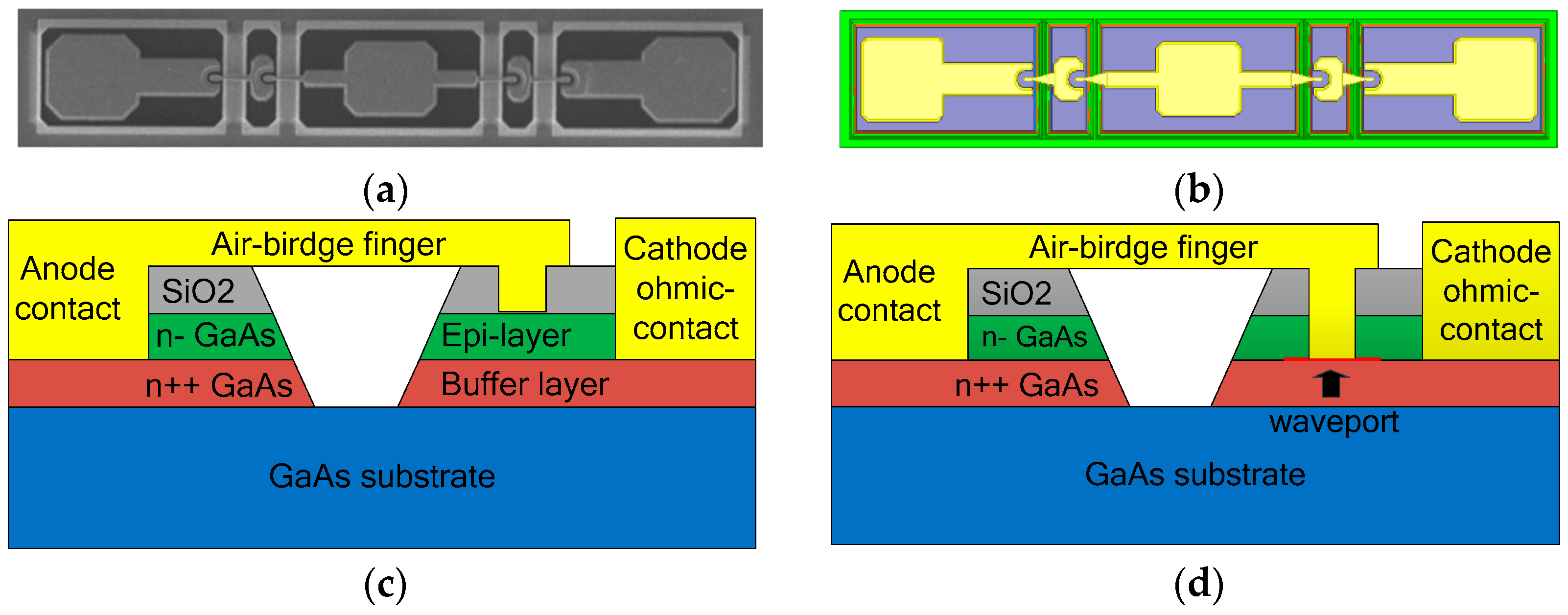
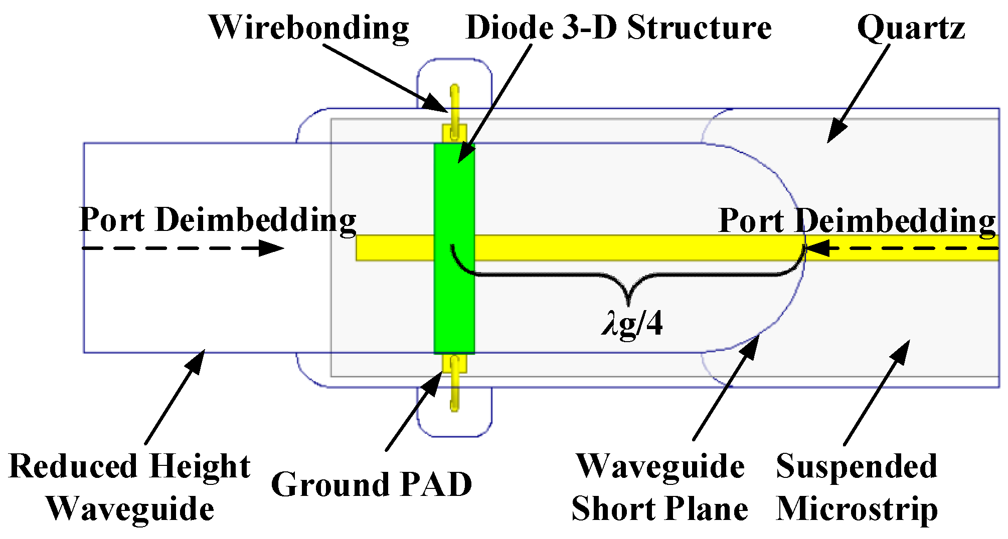
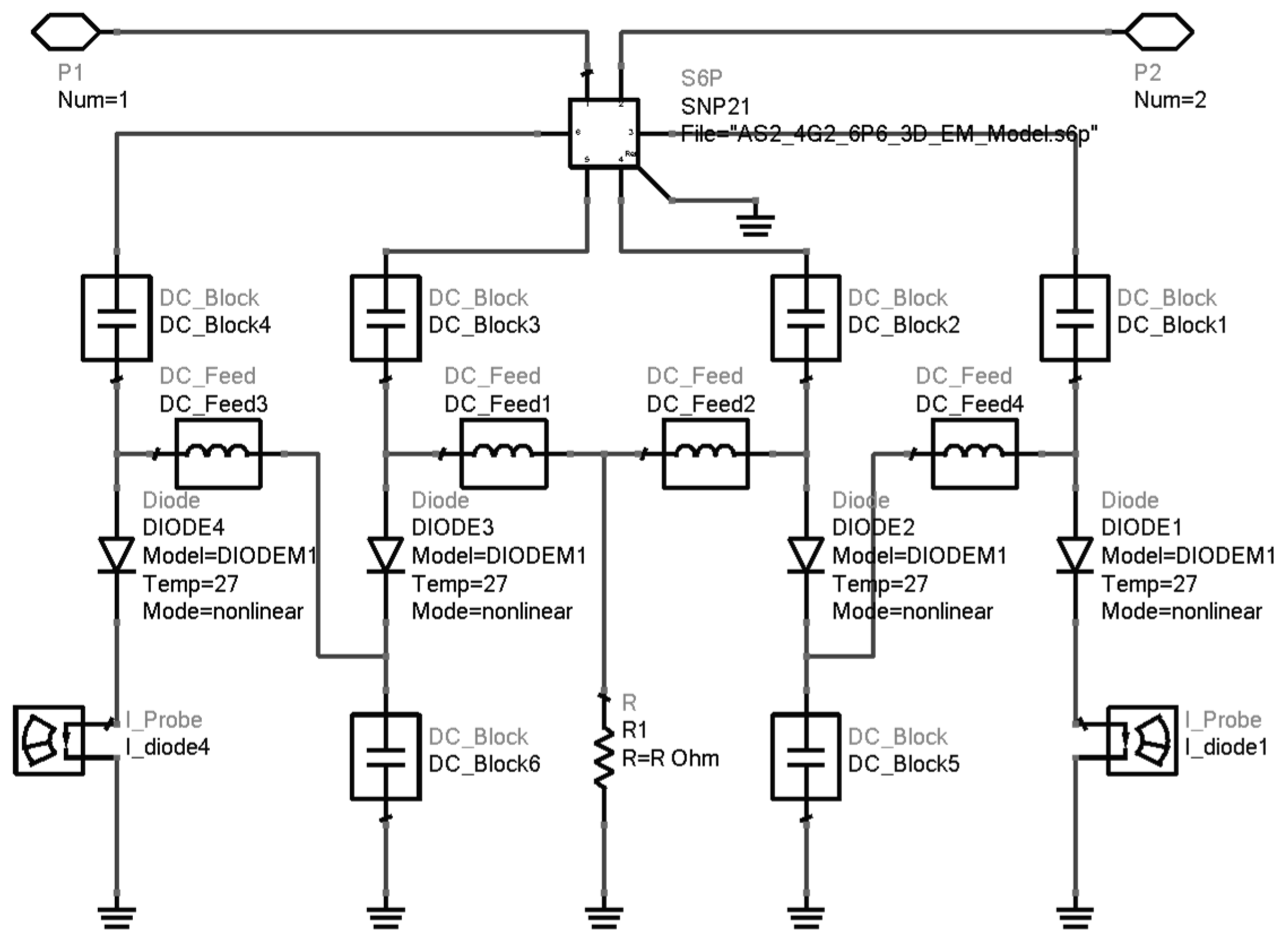
2.1. Diode Modeling
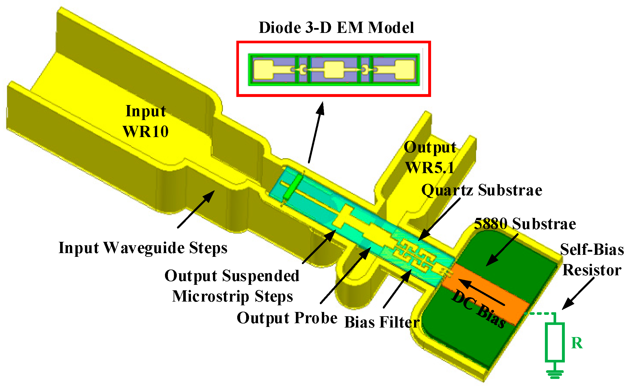
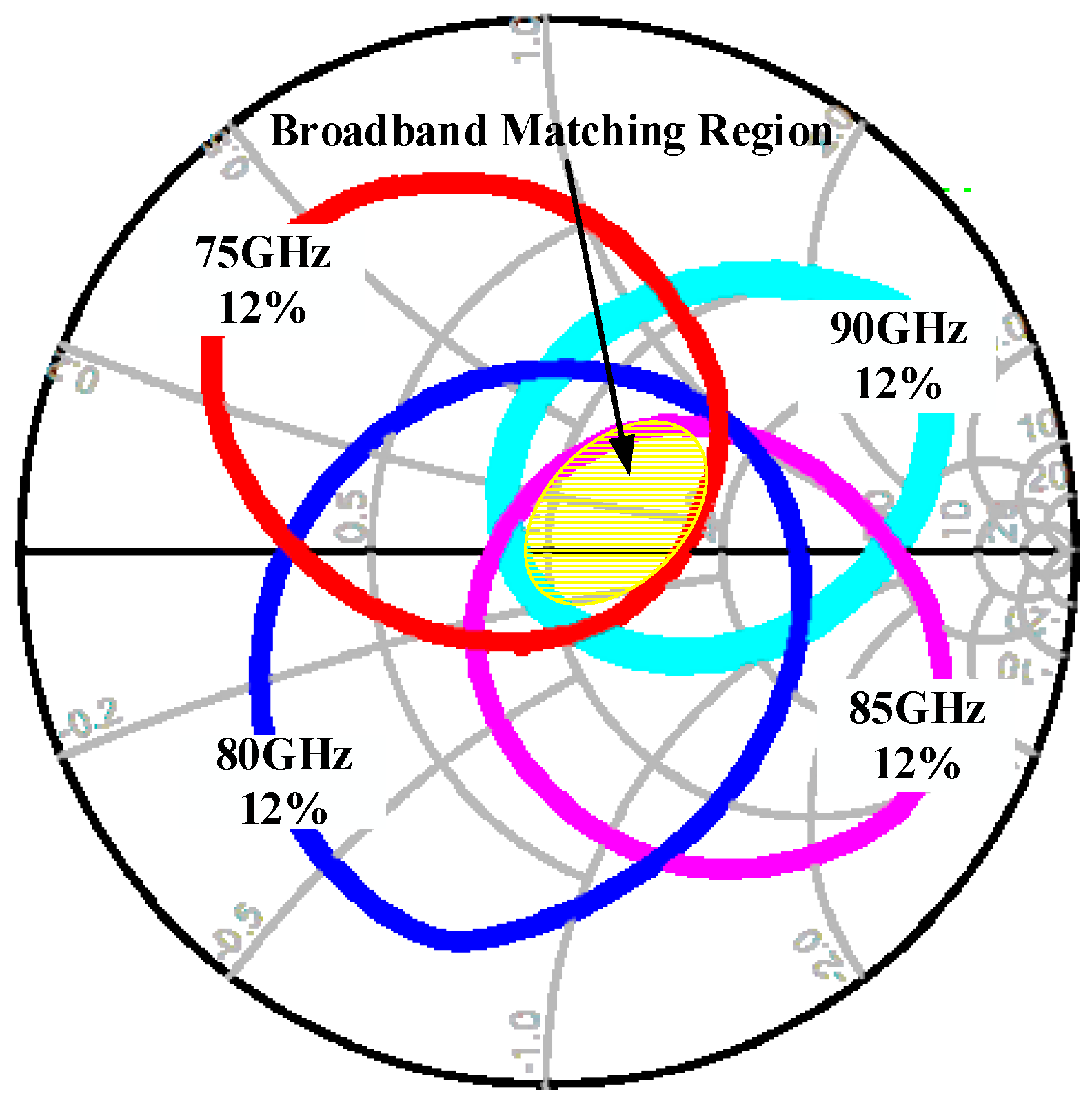
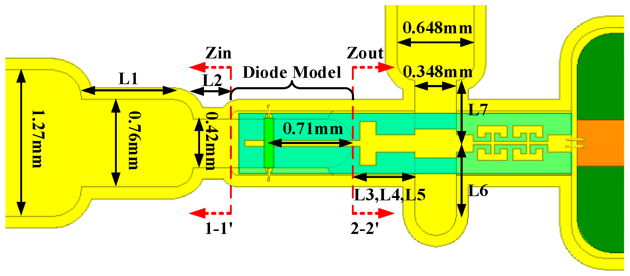
2.2. Doubler Design
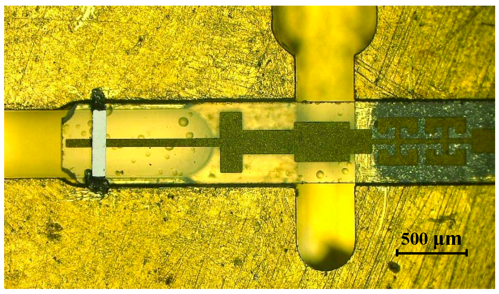
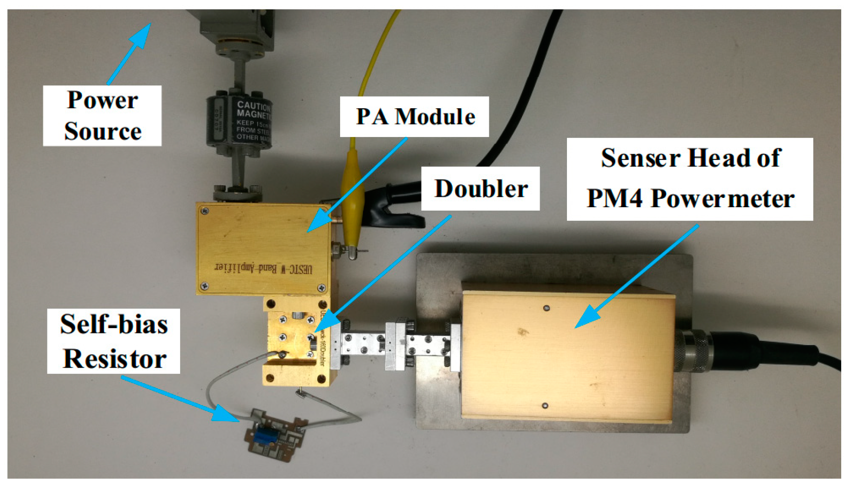
2.3. Fabrication and Measurement
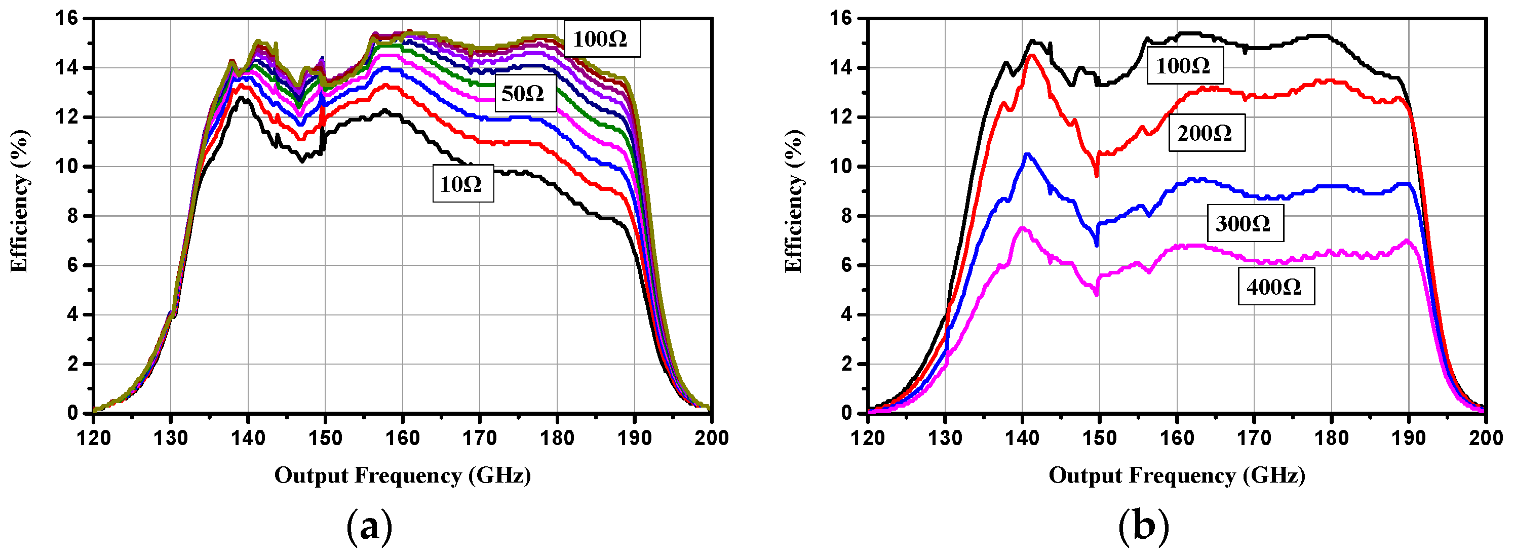
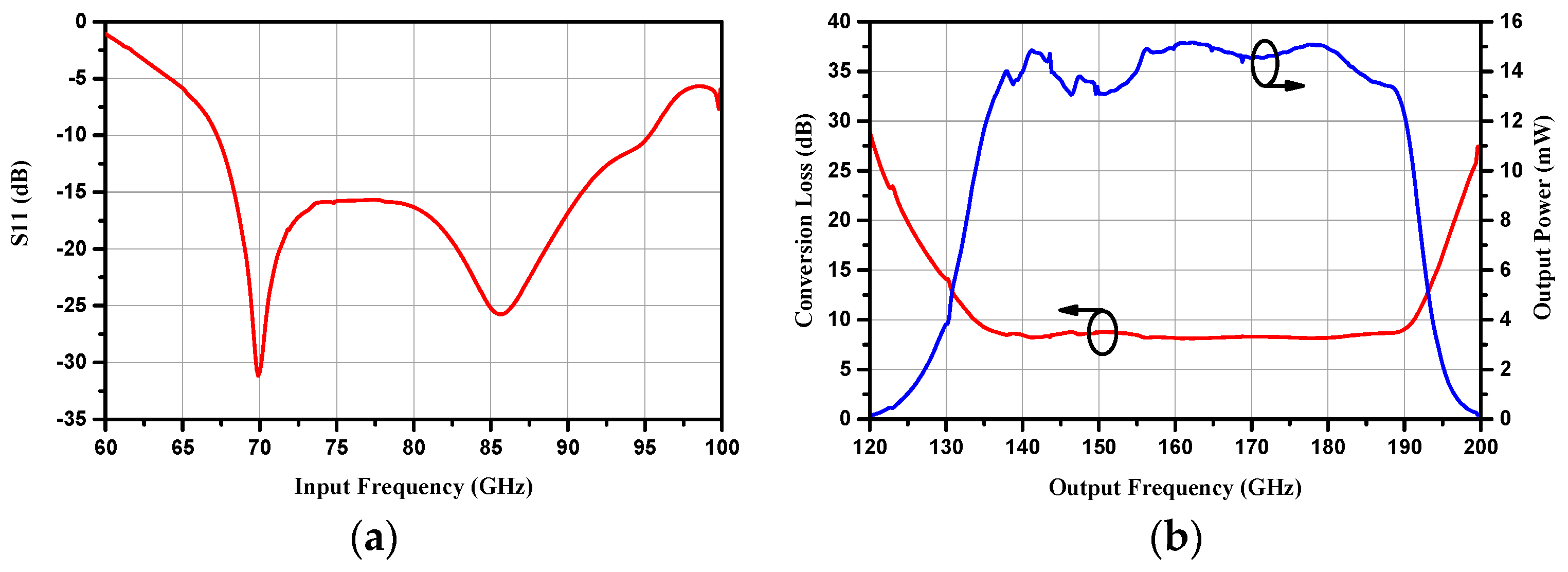
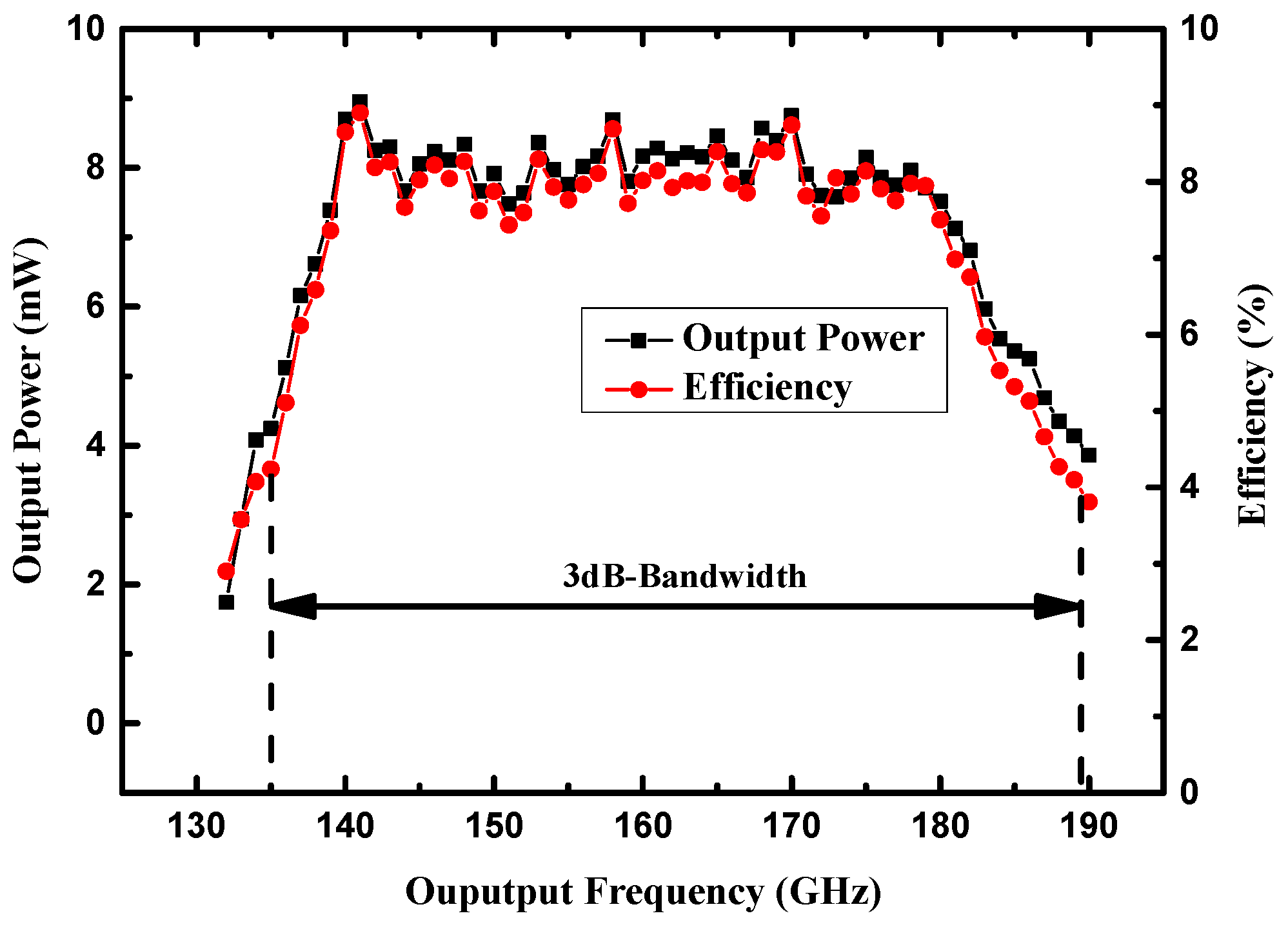
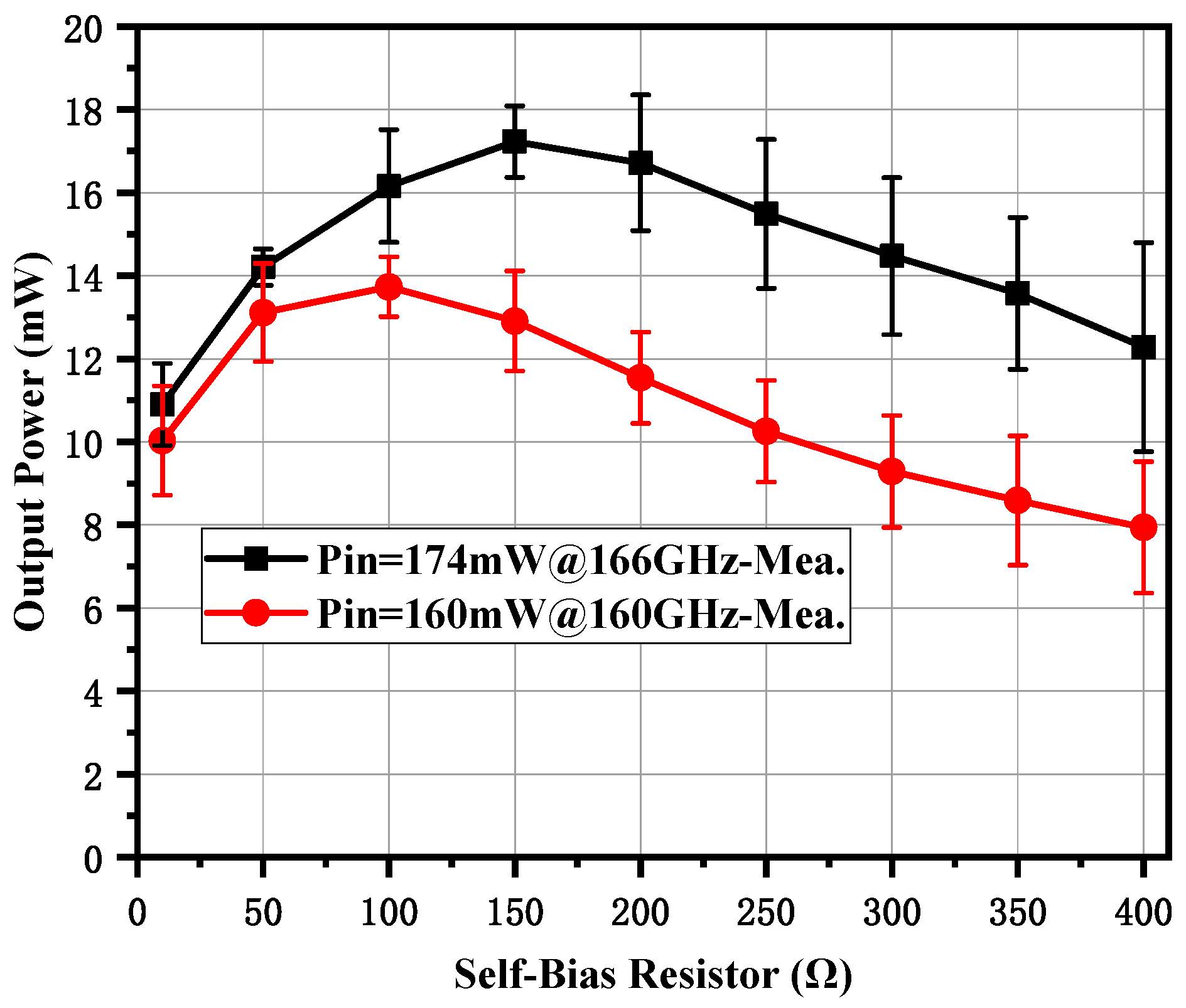
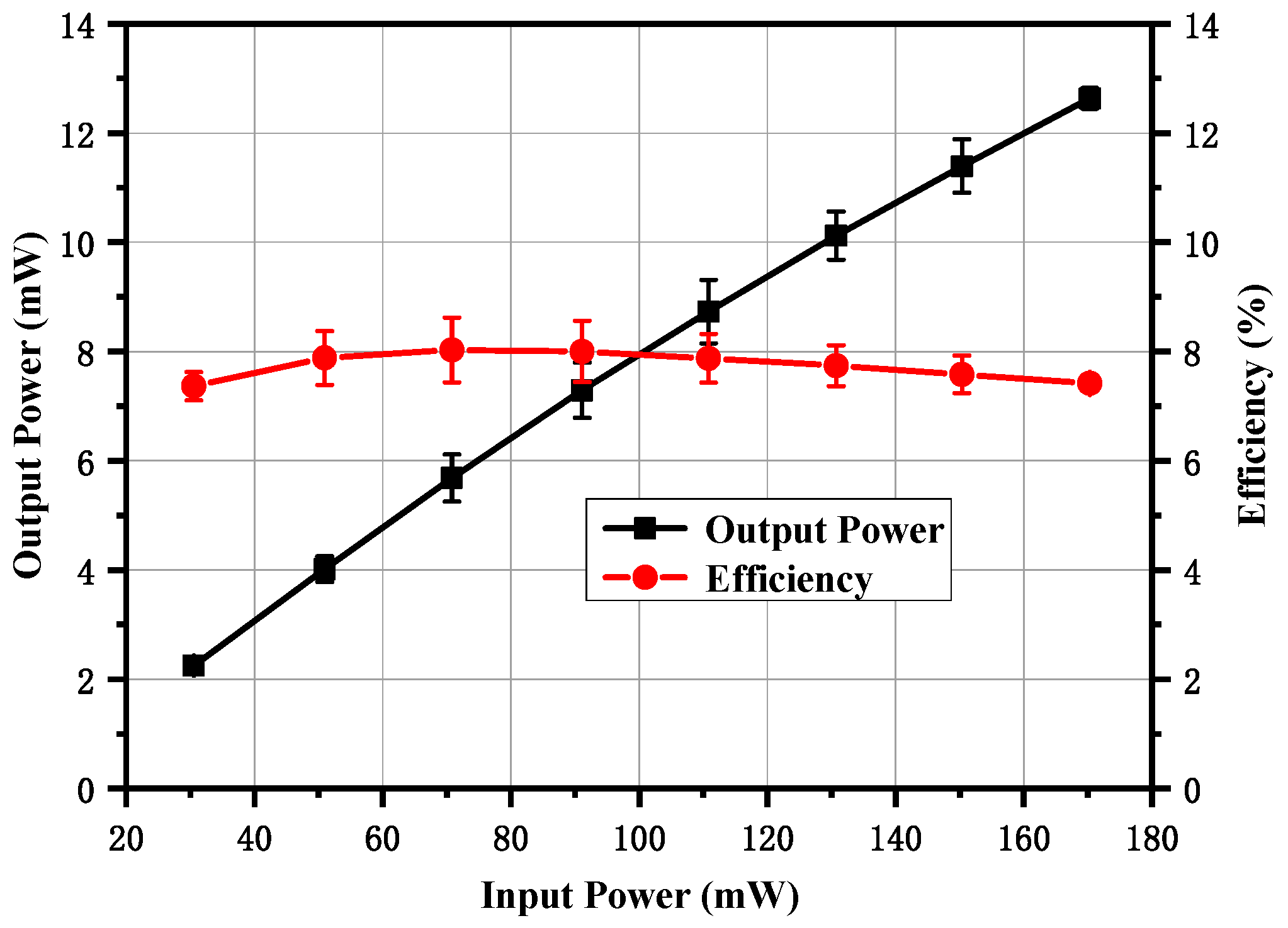
3. Results and Discussion
4. Conclusions
Author Contributions
Funding
Conflicts of Interest
References
- Siegel, P.H. Terahertz technology. IEEE Trans. Microw. Theory Tech. 2002, 50, 910–928. [Google Scholar] [CrossRef]
- Song, H.; Nagatsuma, T. Present and Future of Terahertz Communications. IEEE Trans. Terahertz Sci. Technol. 2011, 1, 256–263. [Google Scholar] [CrossRef]
- Paoloni, C.; Di Carlo, A.; Brunetti, F.; Mineo, M.; Ulisse, G.; Durand, A.; Krozer, V.; Kotiranta, M.; Fiorello, A.M.; Dispenza, M.; et al. Design and Fabrication of a 1 THz Backward Wave Amplifier. Terahertz Sci. Technol. 2011, 4, 149–163. [Google Scholar]
- Samoska, L.A. An Overview of Solid-State Integrated Circuit Amplifiers in the Submillimeter-Wave and THz Regime. IEEE Trans. Terahertz Sci. Technol. 2011, 1, 9–24. [Google Scholar] [CrossRef] [Green Version]
- Chattopadhyay, G. Technology, Capabilities, and Performance of Low Power Terahertz Sources. IEEE Trans. Terahertz Sci. Technol. 2011, 1, 33–53. [Google Scholar] [CrossRef]
- Maestrojuan, I.; Ederra, I.; Gonzalo, R. Fourth-Harmonic Schottky Diode Mixer Development at Sub-Millimeter Frequencies. IEEE Trans. Terahertz Sci. Technol. 2015, 5, 518–520. [Google Scholar] [CrossRef]
- Sadeghzadeh, R.A.; Alibakhshi-Kenari, M.; Naser-Moghadasi, M. UWB antenna based on SCRLH-TLs for portable wireless devices. Microw. Opt. Technol. Lett. 2016, 58, 69–71. [Google Scholar] [CrossRef]
- Alibakhshikenari, M.; Virdee, B.S.; Khalily, M.; Shukla, P.; See, C.H.; Abd-Alhameed, R.A.; Falcone, F.; Limiti, E. Beam-scanning leaky-wave antenna based on CRLH-metamaterial for millimeter-wave applications. IET Microw. Antennas Propag. 2019. [Google Scholar] [CrossRef]
- Liu, Y.; Lu, H.; Wu, Y.; Cui, M.; Li, B.; Zhao, P.; Lv, X. Millimeterwave and Terahertz Waveguide-Fed Circularly Polarized Antipodal Curvedly Tapered Slot Antennas. IEEE Trans. Antennas Propag. 2016, 64, 1607–1614. [Google Scholar] [CrossRef]
- Deng, X.; Li, Y.; Liu, C.; Wu, W.; Xiong, Y. 340 GHz On-Chip 3-D Antenna With 10 dBi Gain and 80% Radiation Efficiency. IEEE Trans. Terahertz Sci. Technol. 2015, 5, 619–627. [Google Scholar] [CrossRef]
- Hirata, A.; Kosugi, T.; Takahashi, H.; Takeuchi, J.; Togo, H.; Yaita, M.; Kukutsu, N.; Aihara, K.; Murata, K.; Sato, Y.; et al. 120-GHz-Band Wireless Link Technologies for Outdoor 10-Gbit/s Data Transmission. IEEE Trans. Microw. Theory Tech. 2012, 60, 881–895. [Google Scholar] [CrossRef]
- Ducournau, G.; Szriftgiser, P.; Beck, A.; Bacquet, D.; Pavanello, F.; Peytavit, E.; Zaknoune, M.; Akalin, T.; Lampin, J.F. Ultrawide-Bandwidth Single-Channel 0.4-THz Wireless Link Combining Broadband Quasi-Optic Photomixer and Coherent Detection. IEEE Trans. Terahertz Sci. Technol. 2014, 4, 328–337. [Google Scholar] [CrossRef]
- Li, C.; Ko, C.; Kuo, M.; Chang, D. A 340-GHz Heterodyne Receiver Front End in 40-nm CMOS for THz Biomedical Imaging Applications. IEEE Trans. Terahertz Sci. Technol. 2016, 6, 625–636. [Google Scholar] [CrossRef]
- Chattopadhyay, G.; Schlecht, E.; Ward, J.S.; Gill, J.J.; Javadi, H.H.; Maiwald, F.; Mehdi, I. An all-solid-state broad-band frequency multiplier chain at 1500 GHz. IEEE Trans. Microw. Theory Tech. 2004, 52, 1538–1547. [Google Scholar] [CrossRef]
- Crowe, T.W.; Bishop, W.L.; Porterfield, D.W.; Hesler, J.L.; Weikle, R.M. Opening the terahertz window with integrated diode circuits. IEEE J. Solid State Circuits 2005, 40, 2104–2110. [Google Scholar] [CrossRef]
- Mehdi, I.; Siles, J.V.; Lee, C.; Schlecht, E. THz Diode Technology: Status, Prospects, and Applications. Proc. IEEE 2017, 105, 990–1007. [Google Scholar] [CrossRef]
- Hesler, J.L.; Hall, W.R.; Crowe, T.W.; Weikle, R.M.; Deaver, B.S.; Bradley, R.F.; Pan, S.K. Fixed-tuned submillimeter wavelength waveguide mixers using planar schottky-barrier diodes. IEEE Trans. Microw. Theory Tech. 1997, 45, 653–658. [Google Scholar] [CrossRef]
- Siles, J.V.; Grajal, J. Physics-Based Design and Optimization of Schottky Diode Frequency Multipliers for Terahertz Applications. IEEE Trans. Microw. Theory Tech. 2010, 58, 1933–1942. [Google Scholar] [CrossRef]
- Xu, H.; Schoenthal, G.S.; Liu, L.; Xiao, Q.; Hesler, J.L.; Weikle, R.M. On Estimating and Canceling Parasitic Capacitance in Submillimeter-Wave Planar Schottky Diodes. IEEE Microw. Wirel. Compon. Lett. 2009, 19, 807–809. [Google Scholar] [CrossRef]
- Tang, A.Y.; Stake, J. Impact of Eddy Currents and Crowding Effects on High-Frequency Losses in Planar Schottky Diodes. IEEE Trans. Electron Devices 2011, 58, 3260–3269. [Google Scholar] [CrossRef] [Green Version]
- Tang, A.Y.; Schlecht, E.; Lin, R.; Chattopadhyay, G.; Lee, C.; Gill, J.; Mehdi, I.; Stake, J. Electro-Thermal Model for Multi-Anode Schottky Diode Multipliers. IEEE Trans. Terahertz Sci. Technol. 2012, 2, 290–298. [Google Scholar] [CrossRef]
- Siles, J.V.; Maestrini, A.; Alderman, B.; Davies, S.; Wang, H.; Treuttel, J.; Leclerc, E.; Narhi, T.; Goldstein, C. A Single-Waveguide In-Phase Power-Combined Frequency Doubler at 190 GHz. IEEE Microw. Wirel. Compon. Lett. 2011, 21, 332–334. [Google Scholar] [CrossRef]
- Ding, J.; Maestrini, A.; Gatilova, L.; Cavanna, A.; Shi, S.; Wu, W. High Efficiency and Wideband 300 GHz Frequency Doubler Based on Six Schottky Diodes. J. Infrared Millim. Terahertz Waves 2017, 38, 1331–1341. [Google Scholar] [CrossRef]
- Porterfield, D.W. High-Efficiency Terahertz Frequency Triplers. In Proceedings of the 2007 IEEE/MTT-S International Microwave Symposium, Honolulu, HI, USA, 3–8 June 2007. [Google Scholar]
- Liu, H.; Powell, J.; Viegas, C.; Pérez-Moreno, C.G.; Alderman, B. A 40 to 160 GHz high power multiplier chain using planar Schottky diodes. In Proceedings of the 2015 8th UK, Europe, China Millimeter Waves and THz Technology Workshop (UCMMT), Cardiff, UK, 14–15 September 2015. [Google Scholar]
- Chen, Z.; Wang, H.; Alderman, B.; Huggard, P.; Zhang, B.; Fan, Y. 190 GHz high power input frequency doubler based on Schottky diodes and AlN substrate. IEICE Electron. Express 2016, 13, 20160981. [Google Scholar] [CrossRef]
- Yang, F. Discrete schottky diodes based terahertz frequency doubler for planetary science and remote sensing. Microw. Opt. Technol. Lett. 2017, 59, 966–970. [Google Scholar] [CrossRef]
- Guo, C.; Shang, X.; Lancaster, M.J.; Xu, J.; Powell, J.; Wang, H.; Alderman, B.; Huggard, P.G. A 135–150-GHz Frequency Tripler With Waveguide Filter Matching. IEEE Trans. Microw. Theory Tech. 2018, 66, 4608–4616. [Google Scholar] [CrossRef]
- Deng, J.; Yang, Y.; Zhu, Z.; Luo, X. A 140–220-GHz balanced doubler with 8.7–12.7% efficiency. IEEE Microw. Wirel. Compon. Lett. 2018, 28, 515–517. [Google Scholar] [CrossRef]
- Dou, J.; Jiang, S.; Xu, J.; Wang, W. Design of D-band frequency doubler with compact power combiner. Electron. Lett. 2017, 53, 478–480. [Google Scholar] [CrossRef]
- Zhang, B.; Fan, Y.; Zhang, S.X.; Yang, X.F.; Zhong, F.Q.; Chen, Z. 110 GHz high performanced varistor tripler. In Proceedings of the 2012 International Workshop on Microwave and Millimeter Wave Circuits and System Technology, Chengdu, China, 19–20 April 2012. [Google Scholar]
- Hrobak, M.; Sterns, M.; Schramm, M.; Stein, W.; Schmidt, L.-P. Design and fabrication of broadband hybrid GaAs Schottky diode frequency multipliers. IEEE Trans. Microw. Theory Techn. 2013, 61, 4442–4460. [Google Scholar] [CrossRef]
- High Frequency Structure Simulator; HFSS: Canonsburg, PL, USA, 2015.
- Advanced Design System; Agilent Technologies: Santa Clara, CA, USA, 2013.
- Erickson, N. Wideband High Efficiency Planar Diode Doublers. Proc. Ninth Intl. Sypm. Space Thz Techn. 1998, 473–480. [Google Scholar]
- Erickson, N. High efficiency submillimeter frequency multipliers. IEEE Int. Dig. Microw. Symp. 1990, 3, 1301–1304. [Google Scholar]


| Layers of the Diodes | Thickness (μm) | Doping Concentration (cm−3) | Material | Relative Dielectric Constant |
|---|---|---|---|---|
| Semi-Insulating Substrate | 50 | - | GaAs | 12.9 |
| Buffer Layer | 5 | 5 × 10¹⁸ | Pec | 1 |
| Epi-Layer | 0.26 | 2 × 10¹⁷ | GaAs | 12.9 |
| Oxide Layer | 0.5 | - | SiO2 | 4 |
| Ohmic Contact Layer | 0.76 | - | Gold | 1 |
| Anode and Cathode | 1 | - | Gold | 1 |
| Parameters | Value |
|---|---|
| Reverse Saturation Current, Is | 9.39 × 10⁻¹⁵ A |
| Series Resistance, Rs | 4.1 Ω |
| Ideal Factor, N | 1.12 |
| Zero-biased Junction Capacitance, Cj0 | 9.8 fF |
| Junction Potential, Vj | 0.85 V |
| Reverse Breakdown Current, Ibr | 1 μA |
| Energy Gap, Eg | 1.43 eV |
| Ref. | Frequency (GHz) | Number of Anodes | Pin (mW) | Pout (mW) | Effi. (%) | FBW (%) | Bias Way |
|---|---|---|---|---|---|---|---|
| [22] | 177–202 | 6 × 2 | 20–120 | 1–12 | 4.3–10.2 | 22 | Zero Bias |
| [24] | 200–235 | 6 | 20–60 | 1.5–15 | ~16 | 24 | External Bias |
| [25] | 150–170 | 6 | 10–200 | 1–35 | 5.1–23.5 | 10 | External Bias |
| [26] | 190–198 | 6 | 100–260 | 3.7–20 | 1.4–8 | 4 | External Bias |
| [27] | 180–200 | 6 | 50–95 | 4–13 | 4–10 | 10.5 | External Bias |
| [29] | 140–220 | 2 | 20–32 | 1.8–3.7 | 8.7–12.7 | 44 | Zero Bias |
| This Work | 135–190 | 4 | 30–174 | 2.1–17.8 | 4–10.2 | 34 | Self Bias |
© 2019 by the authors. Licensee MDPI, Basel, Switzerland. This article is an open access article distributed under the terms and conditions of the Creative Commons Attribution (CC BY) license (http://creativecommons.org/licenses/by/4.0/).
Share and Cite
Wu, C.; Zhang, Y.; Cui, J.; Li, Y.; Xu, Y.; Xu, R. A 135-190 GHz Broadband Self-Biased Frequency Doubler using Four-Anode Schottky Diodes. Micromachines 2019, 10, 277. https://doi.org/10.3390/mi10040277
Wu C, Zhang Y, Cui J, Li Y, Xu Y, Xu R. A 135-190 GHz Broadband Self-Biased Frequency Doubler using Four-Anode Schottky Diodes. Micromachines. 2019; 10(4):277. https://doi.org/10.3390/mi10040277
Chicago/Turabian StyleWu, Chengkai, Yong Zhang, Jianhang Cui, Yukun Li, Yuehang Xu, and Ruimin Xu. 2019. "A 135-190 GHz Broadband Self-Biased Frequency Doubler using Four-Anode Schottky Diodes" Micromachines 10, no. 4: 277. https://doi.org/10.3390/mi10040277