Article

A Single DC Source Five-Level Switched Capacitor Inverter for Grid-Integrated Solar Photovoltaic System: Modeling and Performance Investigation

by
Md. Tariqul Islam
1,
Md. Ahsanul Alam
1,
Molla Shahadat Hossain Lipu
1,*,
Kamrul Hasan
2,
Sheikh Tanzim Meraj
3,
Hasan Masrur
4 and
Md. Fayzur Rahman
1
1
Department of Electrical and Electronic Engineering, Green University of Bangladesh, Dhaka 1207, Bangladesh
2
School of Electrical Engineering, College of Engineering, Universiti Teknologi MARA, Shah Alam 40450, Malaysia
3
Department of Electrical and Electronic Engineering, Universiti Teknologi PETRONAS, Seri Iskandar 32610, Malaysia
4
Interdisciplinary Research Center of Smart Mobility and Logistics, King Fahd University of Petroleum and Minerals, Dhahran 31261, Saudi Arabia
*
Author to whom correspondence should be addressed.
Sustainability 2023, 15(10), 8405; https://doi.org/10.3390/su15108405
Submission received: 6 April 2023 / Revised: 6 May 2023 / Accepted: 17 May 2023 / Published: 22 May 2023

Abstract

:
Boost converters and multilevel inverters (MLI) are frequently included in low-voltage solar photovoltaic (PV) systems for grid integration. However, the use of an inductor-based boost converter makes the system bulky and increases control complexity. Therefore, the switched-capacitor-based MLI emerges as an efficient DC/AC voltage convertor with boosting capability. To make classical topologies more efficient and cost-effective for sustainable power generation, newer topologies and control techniques are continually evolving. This paper proposes a reduced-component-count five-level inverter design for generating stable AC voltages for sustainable grid-integrated solar photovoltaic applications. The proposed topology uses seven switching devices of lower total standing voltage (TSV), three diodes, and two DC-link capacitors to generate five-level outputs. By charging and discharging cycles, the DC capacitor voltages are automatically balanced. Thus, no additional sensors or control circuitry is required. It has inherent voltage-boosting capability without any input boost converter. A low-frequency-based half-height (HH) modulation technique is employed in the standalone system for better voltage quality. Extensive simulations are performed in a MATLAB/Simulink environment to estimate the performance of the proposed topology, and 17.58% THDs are obtained in the phase voltages. Using a small inductor in series or an inductive load, the current THD reduces to 8.23%. Better dynamic performance is also observed with different loading conditions. A miniature five-level single-phase laboratory prototype is developed to verify the accuracy of the simulation results and the viability of the proposed topology.

1. Introduction

Environmental concern, increasing fuel prices, and growing load demand led to the transformation of electricity generation in past two decades with more and more renewable energy sources feeding into the grid [1]. The grid-connected solar PV systems necessitate high-power medium-voltage inverters for converting DC to AC at the correct amplitude and frequency [2,3]. The conventional solar power generation system generally uses a step-up transformer, a boost converter, and a line filter as shown in Figure 1. Utilizing these components makes the system bulky, less efficient, and increases cost and operational difficulty [4]. It is essential that inverters are highly reliable and effective to minimize the cost of return without compromising quality [5]. Although a two-level inverter produces a quasi-square wave, its output contains a high value of THD (48.21%) requiring large filters and is also less efficient [6,7].
Following the invention of the first three-level inverter in 1975 [8], various multilevel inverter (MLI) topologies, such as the cascaded H-bridge (CHB), neutral-point-clamped (NPC), flying capacitor (FC), and modular multilevel converter (MMC) were suggested [9]. All of these have common attractive characteristics such as better output voltage quality, a lower device voltage rating, higher efficiency, better power loss distribution, lower harmonic distortion, lower dv/dt, lower EMI, and suitability for medium voltage or high voltage application. All these benefits can be obtained at the expense of a higher number of power switches and other passive components, also requiring complicated modulation and control circuitry. The FC MLI employs balancing capacitors on phase buses, which are clamped by capacitors rather than diodes. The CHB is widely used because of its modular design and greater flexibility. It typically consists of a group of H-bridge cells that may combine the DC voltage from a number of different sources to produce the required voltage [10]. In all topologies, the voltage quality improves as the number of levels increases. However, the control becomes challenging in conventional MLIs because of the exponential rise in the number of driving circuits and components required as the number of levels rises.
PV system demands compact MLIs with boosting capability that can generate low THD voltage. Recently, switched capacitor (SC)-based MLIs emerged as DC/AC voltage convertors with boosting capability. The SC unit has a variable voltage output range that covers an extensive range and depends on the configuration. A conventional active neutral point clamp (ANPC) topology using capacitors was developed in [11]. A sole DC voltage source, eight IGBTs, and three capacitors are required to produce five output voltage levels across the load terminal. Nevertheless, no means of increasing the output voltage is incorporated into this structure. Further ANPC topologies of two distinct varieties were introduced in [12]. These topologies lack voltage-boosting capability and face voltage-balancing problems like conventional NPC and FC topologies. The T-type nested neutral-point-clamped converter (T-NNPC) is a novel architecture suggested by [13] that uses a sole DC supply and four capacitors. This architecture can generate voltage across the load at five distinct levels. The drawbacks of this design are the increased switch voltage and the absence of boosting capability. For motor-driving applications, Ref. [14] presents a five-level H-bridge/NPC (5L-HNPC) structure involving a transformer that is phase-shifted to produce a DC supply with independent voltages for each phase. So, this topology could not be efficient since the transformer makes the system more extensive and expensive. For high-power uses, Ref. [15] presents a five-level nested neutral-point-clamped (5L-NNPC) converter which faces a complex controlling mechanism due to the lack of idleness in the operating states, and this topology entails an advanced model predictive control (MPC) mechanism to regulate the voltage of the flying capacitors under changeable load power factors and modulation indices [16]. A new five-level voltage source inverter (5L-VSI) has been proposed in [17], which uses two DC supplies and three capacitors to generate the desired output voltage. This topology uses high-switching devices and capacitors; therefore, it could not be cost-effective. These things considered, it lacks voltage-boosting capability. In [18], the author offers a ‘dual-T-type five-level inverter’ to mitigate the surge in impulse charging current. This structure’s eight power switches can be modulated to provide voltage at five distinct levels, with a gain of two. Including inductance raises the degree of difficulty in the system. To further minimize the number of IGBTs, a 1-Φ five-level asymmetric hybrid H-bridge inverter is described in [19,20] to reduce the amount of IGBTs, while in [21] a 5L ANPC inverter has been proposed for 1-Φ services. Two inverters’ three-phase extensions need six legs since each phase uses two asymmetrical legs. Thus, the two inverters cannot work with commercial three-level NPC modules. Again, it is seen that most switch capacitor multilevel inverters have faced voltage-balancing problems because of unequal charging and discharging. This problem arises when many capacitors are used with a single DC source. However, a few articles have tried to address this issue. For traditional neutral-point-clamped (NPC) MLI, a voltage-balancing system was implemented based on variables such as, for example, the modulation index (frequency and amplitude) and the power factor. Capacitor voltage balancing, however, becomes more complicated when more levels are added [22,23,24].
Although not easy, adjusting capacitor voltage is essential [25,26]. Therefore, researchers and academicians are now focusing on self-balancing topologies for reducing relevant voltage-balancing problems. In [27], the author proposed a five-level inverter topology that solves the problems of balancing by using two capacitors, inductance, four switching devices, and directional switching. Nevertheless, it lacks voltage-boosting capability. Researchers were intrigued by a proposed modified five-level ANPC inverter [28], which used many capacitors to generate five levels across the load terminal but still required a lot of power. Amplified voltage gain, the balanced voltage across capacitors, and less stress are all benefits of a recently suggested five-level split-midpoint cross-clamped (5L-SMCC) inverter [29]. Moreover, another author presented a novel topology for a five-level ANPC switched capacitor inverter, which would do away with the drawbacks of the traditional five-level ANPC inverter [30]. Despite its self-balancing and voltage-boosting abilities, its total blocking voltage and cost are prohibitive. Scientists are still working hard to perfect a topology that is not just cheap but also capable of boosting and self-balancing [31,32].
This paper proposes a single-phase five-level inverter based on switching capacitors. It is able to achieve an output voltage that is equal to two times the DC input voltage. The switched-capacitor-based inverter design that is being suggested produces five-level output voltages with only two capacitors, one DC source, and seven switching devices. A low-frequency half-height approach is utilized to generate the firing pulses of switching devices in a standalone system for higher output voltage quality and lower THDs. However, for current-controlled grid-integrated solar PV systems, we adopt high-frequency modulation technology because this approach decreases the filter size. However, the salient features of the proposed topology are:
  • Double boosting of output voltage without an inductive element or boost converter suitable for sustainable renewable energy applications.
  • Self-balancing of DC-link capacitor voltage without a controller or sensors.
  • Stable output voltage with lower THD.
  • Simple but effective control of switching devices using the half-height method for a standalone system.
  • A reduced device count and smaller device footprint.
  • Lower voltage stress across the switches.
There are eight main parts to this study. Section 2 outlines the modeling of the proposed multilevel inverter. The proposed MLI’s modulation method and capacitance calculation are covered in Section 3. Section 4 presents the grid-integrated PV system using the proposed inverter, while Section 5 discusses the results from the simulations. Section 6 discusses the results of the experiments. The comparative analysis is presented in Section 7. Finally, Section 8 concludes by summarizing the findings of the proposed work.

2. Proposed Multilevel Inverter Model

2.1. Structure

The structure of the proposed five-level inverter scheme is shown in Figure 2. It consists of 7 switches, 3 diodes, and 2 capacitors. Switches S1–S4 comprise the voltage inversion part, and S5–S7 make the voltage-balancing part. It uses a single DC supply and achieves balanced voltage across the capacitors. It generates stable and double-boosted output voltage with lower THD, making it superior to most other DC-link-based MLIs (such as NPC and FC). It works fairly well under both RL and dynamic loads. Its modular structure allows the generation of more levels via a cascading link.

2.2. Operation

The entire operation of the inverter can be explained using the five different modes, as mentioned in Table 1. Anytime the capacitor is connected in parallel with the source, Vin will be charged to a voltage Vc = Vin (Figure 3a) in a very short time determined by the time constant τ c = r c C i , where rc is the total resistance in the charging path which is very small. When the capacitor is isolated from the source and the load (RL) is connected across it (Figure 3b), it will be discharged slowly determined by the time constant τ d = ( r c + R L ) C i . In the voltage-boosting mode, the capacitor will be connected in series with the load and source (Figure 3c), and both charging and discharging will take place simultaneously.
Details of the different switching modes are shown in Figure 4. The charging path is displayed in green, and the discharging path in blue; the red line represents the capacitor being charged and discharged simultaneously. The operation of each mode is described below:
Mode 1: To achieve a voltage V across capacitor C2, as Figure 4a depicts, we first activate switch S6. Thus, the output voltage is V when switches S1 and S4 are engaged.
Mode 2: Here, the capacitor C1 is charged to V volts by activating switch S7. C2 is discharging at this moment which may cause a slight distortion in the voltage across the load terminal. With the purpose of getting 2V across the load terminal, switches S1, S4, and S5 must be activated. The operation of this mode is depicted in Figure 4b.
Mode 3: By activating switch S6, the capacitor C2 is charged to voltage V. Figure 4c depicts this operation where activating switches S2 and S3 results in an output voltage of −V.
Mode 4: Switch S7 activates capacitors C1 and C2 to produce a 2V voltage in this mode. Currently, C1 is charging and C2 is discharging. As indicated in Figure 4d, switches S2, S3, and S5 must be flipped in order to provide a voltage drop of −2V across the load terminal 4.
Mode 5: As switches S4 and S3 are active, the voltage across the load is zero in this setup. Figure 4e shows a schematic representation of the corresponding circuit. Capacitor C1 is only being charged in this configuration.
The balancing of capacitor voltage can be analyzed through the energy balanced in each capacitor during one complete cycle [33,34]. Figure 5 illustrates the charging and discharging of capacitors in one cycle.
Let us consider that the output voltage and current is a sine function.
V o = V m sin ω t
I o = I m sin ( ω t )
where Vm and Im are the peak values of output voltage and current, and is the phase difference between output voltage and current. Energy stored or released by the DC capacitor is given by Equation (3):
d U = V d q = V I d t               I = d q d t   U = V d q = V I d t  
where I, V, q, and U are the current flowing through capacitor, voltage across, charge, and energy stored by the capacitor, respectively.
The energy sored in the positive half for capacitor C2 can be calculated as follows:
U C 2 + = 0 π V E I m sin ω t d t   = 0 α 1 0 . I m sin ω t d ω t + α 1 α 2 E . I m sin ω t d ω t + α 2 α 3 0 . I m sin ω t d ω t + α 3 α 4 E . I m sin ω t d ω t + α 4 π 0 . I m sin ω t d ω t = E I m [   cos α 1 cos α 2 + cos α 3 cos α 4 ] .
The energy sored in the negative half for capacitor C2 can be calculated as follows:
U C 2 = π 2 π V E I m sin ω t d ω t   = π α 5 0 . I m sin ω t d t + α 5 α 6 E . I m sin ω t d t + α 6 α 7 0 . I m sin ω t d ω t + α 7 α 8 E . I m sin ω t d ω t + α 8 2 π 0 . I m sin ω t d ω t   = E I m [   cos α 6 cos α 5 + cos α 8 cos α 7 ] .
However, α5 =   π   + α1; α6 =   π   + α2; α7 =   π   + α3; α8 =   π   + α4.
So, Equation (5) will be
U C 2 = E I m [   cos α 1 cos α 2 + cos α 3 cos α 4 ] .
Thus, U C 2 + = U C 2   .
This means that the energy stored in the capacitor C2 over the course of a full cycle is balanced and constant, maintaining the capacitor voltage at a constant under all circumstances.
The energy sored in the positive half for capacitor C1 can be calculated as follows:
U C 1 + = 0 π V E I m sin ω t d ω t   = 0 α 1 0 . I m sin ω t d t + α 1 α 2 0 . I m sin ω t d ω t + α 2 α 3 E . I m sin ω t d ω t + α 3 α 4 0 . I m sin ω t d ω t + α 4 π 0 . I m sin ω t d ω t = E I m [   cos α 2 cos α 3 ]
The energy sored in the negative half for capacitor C1 can be calculated as follows:
U C 1 = π 2 π V E I m sin ω t d ω t   = π α 5 0 . I m sin ω t d ω t + α 5 α 6 0 . I m sin ω t d ω t + α 6 α 7 E . I m sin ω t d ω t + α 7 α 8 0 . I m sin ω t d ω t + α 8 2 π 0 . I m sin ω t d ω t   = E I m [   cos α 7 cos α 6 ]
However, α5 =   π   + α1; α6 =   π   + α2; α7 =   π   + α3; α8 =   π   + α4.
So, the Equation (8) will be
U C 1 = E I m [   c o s α 2 cos α 3 ] .
Thus, U C 1 + = U C 1 .
This means that the energy stored in the capacitor C1 over the course of a full cycle is balanced and constant, maintaining the capacitor voltage at a constant under all circumstances.

2.3. Three-Phase Arrangement of Proposed Inverter

This subsection details the five-level inverter’s proposed three-phase setup. As can be seen in Figure 6, a single-phase inverter is used to convert the DC-link voltage into a variable five-level output voltage. Since the proposed inverter has a voltage gain of 2, the DC-link voltage should be higher than the inverter output voltage (>Vo/ 2 ). An inverter’s ability to ensure power flow to the load depends on meeting these criteria. The three-phase transformer’s neutral points are then shorted, and a trio of single-phase five-level inverters is connected to the 12 terminals. The primary benefits include a greater output voltage with fewer active components, a smaller transformer, a direct current (DC) input source, and less complicated control circuits. This inverter’s fault detection and device replacement processes are simple.

3. Modulation Technique

Generating suitable switching signals for the power devices is an integral part of the MLI modulation method. Since switching losses and total harmonic distortion are so closely related, it has a pronounced influence on the converter’s efficiency and THDs. Several modulation strategies have been developed to improve harmonic performance while reducing losses; these techniques all make use of either the fundamental switching frequency and/or the high switching frequency [35]. In some cases, discontinuous PWM schemes are also proposed for better DC bus utilization [34]. Again, in some papers, a combination of two frequency signals (low and high) has been used to generate firing pulses of multilevel inverters to produce lower switching losses [36]. However, in the low switching frequency range, only one or two switching pulses occur per round, but in the high switching frequency range, numerous switching pulses occur per round [37]. A fundamental frequency modulation strategy was adopted for this study due to its low total harmonics distortion. The half-height method has the lowest THD value [38,39]. In this method, when the value of the sine function hits halfway between the minimum and maximum levels, a switching angle is set. In this technique, the output more closely resembles a sine wave. Following Figure 7, the general formula for determining the principal switching angles in the first quadrant (from 0 to 90°) is given below [39]:
α i = sin 1 ( 2 i 1 N 1 ) w h e r e   i = 1 , 2 , 3 . . N 1 2
where N is the number of levels.
For the suggested topology, the main switching angles (0–90°) are
α 1 = sin 1 ( 2 1 4 ) = 14.48 ° ,     α 2 = sin 1 ( 2 × 2 1 4 ) = 48.59 ° .  
Other switching angle are determined as
α3 = 180° − α2; α4 = 180° − α1; α5 = 180° + α1; α6 = 180° + α2; α7 = 360° − α2; α8 = 360° − α1.
The switching arrangements of the designed topology using the half-height method are depicted in Figure 8. The calculated angle is tabulated in Table 2.

Calculation of Capacitance

The capacitor values are determined through the calculation of worst discharge time t1 and t2, as shown in Figure 7 [40]:
t 1 = sin 1 1 2 2 π f
t 2 = π sin 1 1 2 2 π f   .
The maximum discharge quantity of the capacitor (ΔQc) is calculated as
Δ Q c = t 1 t 2 I p e a k S i n 2 π f t d t   .
Now, the maximum capacitor value is given by
C Δ Q c k . V d c
where k is the ripple ratio.

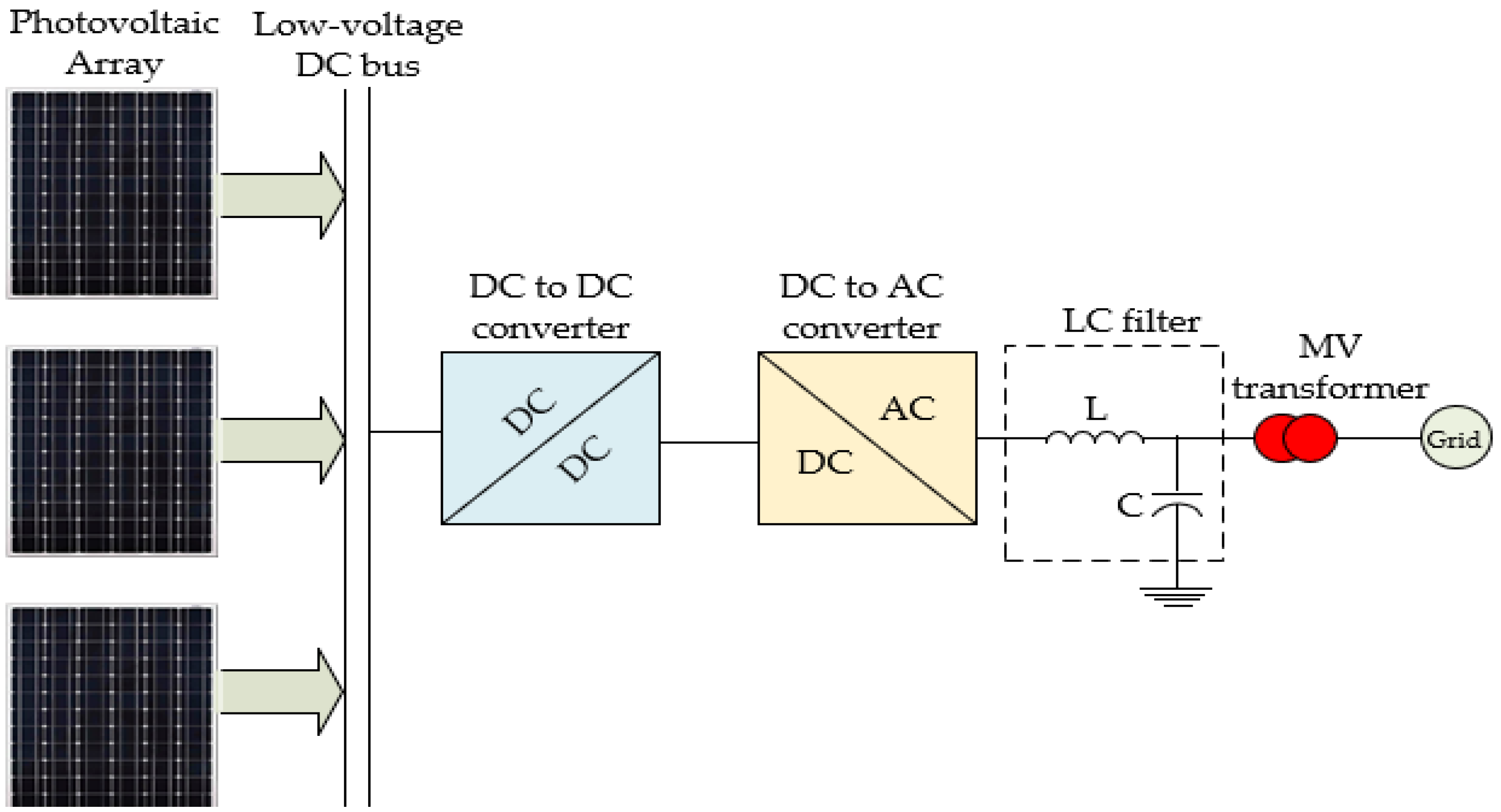
4. Grid-Integrated Solar Photovoltaic System with Proposed Multilevel Inverter

A single-phase grid-integrated solar PV system interfaced with proposed MLI is shown in Figure 9.
The input of this PV system employs only 6 series-connected modules per string and 4 parallel strings to generate 230 V(rms). Eliminating the boost converter and its large inductor reduces the cost and footprint of the PV system. In order to get rid of excessive total harmonics distortion, the inverter’s output is fed into an LCL filter circuit before being connected to the grid. Because of its superior attenuation at the system’s high switching frequency, the LCL filter is chosen here. To regulate the flow of current through the inverter and the grid, a proportional resonance controller (PR) current controller is employed. The controller parameters Kp = 500, Kr = 100, and ω2/Kr = 986.83 are determined through trial and error for optimum performance. The PR converter’s output is then added to the grid voltage and the resulting voltage is divided by Vdc to give Vref. The proposed inverter circuit’s firing pulses are then derived by comparing the Vref voltage to various carrier signals prepared using the phase disposition (PD) approach. In this grid-integrated system, it is difficult to control the current of the proposed grid connected system using the half-height method, although it works perfectly on a standalone system. For this reason, the PD method is used for the proposed grid connected system.

4.1. Selection of Solar PV Array

The PV system is designed for a 230 V(rms) AC system with a peak power capacity of 1 kW. The 1Soltech 1STH-215-P model is chosen from the PV array library to obtain the necessary parameters PmpA, ImpT, and VOCA. It features an open circuit module voltage (Voc) of 36.3 V and a 7.84 A short circuit module current (Isc). Taking into account the PV array’s open circuit voltage VOCA = 200 V and power PmpA = 1 kW, the PV modules connected in a series string are estimated as [41]
N s = V d c V o c = 200 36.3 6   .
The maximum current of the solar PV array is given as
I m p T = P m p A 0.85 × V O C = 32.41   A   .
The PV modules connected in a parallel string are estimated as
N p = I m p T I s c = 32.41 7.84 4   .

4.2. Calculation of Filters Parameters

Consider P = rated active power, Vg = grid voltage, Vdc = DC-link voltage, f = grid frequency, fsw = switching frequency, and fres = resonance frequency. Thus, the filter values will be referred to in a percentage of the base values [42]
Z b = v g 2 P
C b = 1 2 π f Z b   .
Considering allowable output current ripple up to 10%, the inverter side inductance, Li, is calculated as [42]
L i = V D C 16 × f s × Δ I   L m a x
where Δ I L m a x is the 10% current ripple and is given by
  Δ I L m a x = 0.01 × 2 × P V g   .
Considering a maximum of 5% grid power factor variation, the filter capacitor is given by
Δ C f = 0.05 × C b   .
The grid side inductance L g can be calculated as
L g = r × L i   .
The resonant frequency for the filter circuit can be calculated as
f r e s = 1 2 π L i + L g L i   × L g × C f
where f r e s must be 10 f < f r e s < 0.5   f s w .
Figure 10a illustrates the LCL filter’s frequency response. The noticeable sharp peak at the resonance frequency as well as the opposite sign in gain margin and phase margin confirms the instability of the system. A damping resistor is added in series with the capacitor (Cf), to decrease this sharp peak, and it is calculated using the following the equation:
R s d = 1 3 × 2 π × f r e s × C f   .
As shown in Figure 10b, this damping resistor makes the gain margin and phase margin of the same sign and, thus, stabilizes the system.

5. Results and Discussion

The performances of the standalone system and grid-integrated system were evaluated through extensive simulations using MATLAB/SIMULINK. Table 3 contains all of the simulation parameters. The full simulation results are presented below.

5.1. Simulation Results of Standalone System

This subsection presents the simulation results of the standalone system. Figure 11 illustrates the switching pulses of several different switches. The voltage across the capacitors (C1 and C2) is depicted in Figure 12. It shows that VC1 is quite stable all throughout the simulation time frame. While VC2 does suffer a slight discharge if the load current is flowing, it soon recovers during the next charging cycle. For this reason, its functioning is consistently reliable. The responses (voltage and current) for a constant resistive load (ZL = 200 Ω) are depicted in Figure 13 and Figure 14, respectively. The voltage and current are perfectly in phase, as evidenced by the THD measurement of 17.58%. Using a small LCL filter, this can be brought down to below 5%. Figure 15 and Figure 16 present that the THD value of the output current drops to 8.23% when a resistive inductive load (R = 200 Ω, L = 100 mH) is connected due to the inductive effect.
To assess the performance with dynamic load change, ZL is varied from no load to Z1 (R = 200 Ω, L = 100 mH), then down to Z2 (R = 100 Ω, L = 50 mH), and then again back up to Z1 (R = 200 Ω, L = 100 mH). From the voltage and current responses, as shown in Figure 17, it is clear that the voltage remains consistently constant while the current follows the load variations. This shows excellent voltage regulation due to dynamic load. However, the three-phase output voltage, current, and THD profile are depicted in Figure 18. The THD generated by the inverter is about 0.25% using the half-height method.

5.2. Simulation Results of Grid-Integrated Solar Photovoltaic System

This subsection represents the detailed simulation results of the proposed grid-integrated solar photovoltaic system. A solar panel consisting of six series and four parallel strings are used to generate 200 volts across the DC-link capacitor of the solar panel. Figure 19a shows that the DC-link capacitor voltage remains at the designed value. The self-balancing capacitors voltages also maintain the same value as can be seen in Figure 19b and Figure 19c, respectively.
Figure 19d represents the output voltage (≈400 V) response of the proposed five-level inverter before the LCL filter. This double boosting eliminates the need for a boost converter with large size inductor and associated control circuits. These are the main merits of the proposed inverter.
The current controller (PR), designed in Section 4, is used to control the current in the proposed system. Figure 19e,f shows the grid current and inverter current, respectively. From these figures, it is seen that the grid voltage, grid current, and inverter current are in phase which reflects the perfect synchronization.
After analyzing these simulation results it can be concluded that the five-level inverter works fairly well under dynamic loads. These features, along with voltage boosting and self-balancing of the capacitor voltage, will make it a viable option for sustainable development.

6. Experimental Results

A small prototype is developed to validate the theoretical analysis of the suggested structure portrayed in Figure 20. Table 4 lists the design parameters and component specifications. Arduino UNO based a low-cost microcontroller is used to produce switching signals using the half-height technique. Figure 21 demonstrates the gate pulse voltages of several distinct types of switches. Figure 22 displays the voltage across two DC-link capacitors. Figure 23 illustrates the voltage across the load of the suggested structure, which is quite close to the simulation result in Figure 13.

7. Performance Comparative Analysis

The suggested topology is statistically compared to conventional five-level inverters with regard to the component count, voltage gain, total blocking voltage, and balancing capacity. As depicted in Figure 24, the number of switching devices the designed structure requires to generate all five levels is lower than any existing topologies. Despite having three more diodes than the DC and FC MLI topologies, the suggested architecture only requires two DC-link voltages. In contrast to CHB MLI, the suggested topology does not utilize a clamping diode and capacitor. With the suggested topology, a boost converter is not necessary for a grid-integrated system.
Another comparison has been carried out among different switched capacitor five-level inverters and the suggested topology, as shown in Table 5.
The proposed topology uses seven switching devices which is more than Refs. [13,20,27]. The proposed topology uses three diodes which is lower than Refs. [14,30]. In addition, the suggested topology uses only two capacitors to obtain a voltage gain of two. In contrast, Ref. [30] uses three capacitors for a voltage gain of 2. The designed topology also has a low total blocking voltage compared to the topologies described in references [12,20,21,30]. From the above discussion, the suggested topology will be a better choice for a grid-integrated solar photovoltaic system. As can be seen, the proposed topology is more efficient in terms of DC supply, capacitors, and switching devices, while the topologies presented in Refs. [31,32,43] employ less components and have lower TBVs than the proposed topology. However, the design that is suggested only requires a single DC voltage, two capacitors, and seventeen switching devices to generate a three-phase voltage, whereas the other two topologies require three voltage sources, three capacitors, and eighteen switching devices. Therefore, the proposed design will function effectively within a three-phase system. In addition, it is simpler to regulate a single voltage source than it would be to manage three independent DC sources. Since this is also the case for DC voltage regulation, the proposed topology is preferable.
Table 5. Comparison of suggested multilevel inverter with different switch capacitor five-level inverters.
TopologyTotal No. of
SwitchesDiodesCapacitorsInductorTBV(×V)Voltage GainBalancing Capacity
Barbosa et al. [11]8030121No
Soeiro et al. [12]8030141No
Bahrami et al. [13]6040101No
Vazquez et al. [14]8520-1No
Dekka et al. [15] 8220-0.5No
Narimani et al. [16]8220-0.5No
Dekka et al. [17] 10030-0.66No
Lee et al. [18] 10011-2Yes
Valderrama et al. [20] 6020201-
Zhang et al. [21] 8020201-
Ye et al. [27] 6220121Yes
Sathik et al. [30] 7430242Yes
Singh et al. [44]8-1--2Yes
Agarwal et al. [32]611-112Yes
Singh et al. [31]6110-2Yes
Rehman et al. [43]6010-2Yes
Proposed7320122Yes
Another comparison has been made based on the matric of the cost function as defined in [45]. The cost function can be calculated by using the following equation. Here, Nsw, Ndc, Ngd, Nd, Nc, Nl, α, and TBVp.u. are the No. of switches, DC source, gate driver circuit, diode, capacitor, inductor, cost factor, and total blocking voltage per unit, respectively. The overall results of the net cost function have been presented in Figure 25. For this analysis, cost function is assumed to be 1.
CF = ( N s w + N g d + N d + N c + N l + α × T B V p . u . ) × N d c
N C F = C F N L
The figure reveals that the maximum value is found in Ref. [21], while the lowest value is found in Ref. [32]. The proposed topology also achieves the second-lowest value. The proposed topology uses only one DC voltage source and two capacitors, which is less than the three-phase topology (it will use three voltage sources and three capacitors) as presented in Ref. [32], but the proposed topology has a higher net cost function than Ref. [32] for single phase system. So, the proposed topology will be a prospective cost-effective design.

8. Conclusions

A single DC-source, capacitor-based, five-level inverter is developed with double-boosting capability. To generate five-level AC voltage, it uses only seven semiconductor switches, two DC-link capacitors, and three diodes. The switches are operated efficiently through switching signals generated using a simpler low-frequency modulation scheme. A cost-effective but efficient gate pulse generation technique using an Arduino UNO is demonstrated. During each positive and negative half cycle of the generated AC voltage, the capacitors are charged and discharged in a balanced way. So, capacitor voltages are self-balanced without needing extra voltage sensing and control circuits. The generated AC voltage has a THD of 17.58% which yields a current THD of 8.23% with RL load. Excellent dynamic load response demonstrates the inverter’s suitable applicability for a wide range of load variations. The performance of standalone as well as grid-connected single-phase systems have been extensively examined. Through a comparative analysis of device count, component ratings/sizes, output voltage quality (i.e., THD), and voltage-boosting capability, it is revealed that the proposed inverter is quite competitive with regard to contemporary proposed topologies. Boost-converterless and inductorless, this inverter with a capacitor self-balancing arrangement will make an attractive choice for many low- and medium-voltage industries including the grid integration of renewable energy systems. The scalability of the proposed topology for a three-phase system has been outlined. Its performance evaluation will be reported in future publications. Studies on more than five levels as well as higher voltage boosting could be a potential research area. However, the number of capacitors will increase and balancing their voltages will be challenging. In such a case, hybrid topology can be attempted.

Author Contributions

Conceptualization, M.T.I. and M.A.A.; methodology, M.T.I.; writing—original draft preparation, M.T.I. and M.A.A.; writing—review and editing, M.S.H.L., K.H., S.T.M., H.M. and M.F.R.; supervision, M.S.H.L.; project administration, M.S.H.L. All authors have read and agreed to the published version of the manuscript.

Funding

This work did not receive funding.

Institutional Review Board Statement

Not applicable.

Informed Consent Statement

Not applicable.

Data Availability Statement

Not applicable.

Acknowledgments

The authors acknowledge the Green University of Bangladesh for providing laboratory facilities to conduct this research.

Conflicts of Interest

The authors declare no conflict of interest.

References

  1. Gopal, Y.; Birla, D.; Lalwani, M. Reduced switches multilevel inverter integration with boost converters in photovoltaic system. SN Appl. Sci. 2020, 2, 58. [Google Scholar] [CrossRef]
  2. Bughneda, A.; Salem, M.; Richelli, A.; Ishak, D.; Alatai, S. Review of multilevel inverters for PV energy system applications. Energies 2021, 14, 1585. [Google Scholar] [CrossRef]
  3. Poorfakhraei, A.; Narimani, M.; Emadi, A. A review of modulation and control techniques for multilevel inverters in traction applications. IEEE Access 2021, 9, 24187–24204. [Google Scholar] [CrossRef]
  4. Biswas, M.; Biswas, S.P.; Islam, M.R.; Rahman, M.A.; Muttaqi, K.M.; Muyeen, S.M. A New Transformer-Less Single-Phase Photovoltaic Inverter to Improve the Performance of Grid-Connected Solar Photovoltaic Systems. Energies 2022, 15, 8398. [Google Scholar] [CrossRef]
  5. Meraj, S.T.; Yu, S.S.; Rahman, M.S.; Hasan, K.; Lipu, M.S.H.; Trinh, H. Energy management schemes, challenges and impacts of emerging inverter technology for renewable energy integration towards grid decarbonization. J. Clean. Prod. 2023, 405, 137002–137034. [Google Scholar] [CrossRef]
  6. Yarlagadda, A.K.; Eate, V.K.; Babu, Y.S.K.; Chakraborti, A. A modified seven level cascaded H bridge inverter. In Proceedings of the 2018 5th IEEE Uttar Pradesh Section International Conference on Electrical, Electronics and Computer Engineering (UPCON), Gorakhpur, India, 2–4 November 2018; pp. 1–6. [Google Scholar]
  7. Salem, M.; Richelli, A.; Yahya, K.; Hamidi, M.N.; Ang, T.-Z.; Alhamrouni, I. A Comprehensive Review on Multilevel Inverters for Grid-Tied System Applications. Energies 2022, 15, 6315. [Google Scholar] [CrossRef]
  8. Seth, N.; Goel, V.; Kulkarni, R.D.; Joshi, V.P. Performance analysis of seven level three phase asymmetric multilevel Inverter at various modulation indices. In Proceedings of the 2016 International Conference on Electrical Power and Energy Systems (ICEPES), Bhopal, India, 14–16 December 2016; pp. 407–413. [Google Scholar]
  9. Devi, V.S.K.; Srivani, S.G. Modified phase shifted PWM for cascaded H bridge multilevel inverter. In Proceedings of the 2017 Third International Conference on Advances in Electrical, Electronics, Information, Communication and Bio-Informatics (AEEICB), Chennai, India, 27–28 February 2017; pp. 89–94. [Google Scholar]
  10. Ali, A.I.M.; Sayed, M.A.; Takeshita, T. Isolated single-phase single-stage DC-AC cascaded transformer-based multilevel inverter for stand-alone and grid-tied applications. Int. J. Electr. Power Energy Syst. 2021, 125, 106534. [Google Scholar] [CrossRef]
  11. Barbosa, P.; Steimer, P.; Meysenc, L.; Winkelnkemper, M.; Steinke, J.; Celanovic, N. Active neutral-point-clamped multilevel converters. In Proceedings of the 2005 IEEE 36th Power Electronics Specialists Conference, Recife, Brazil, 12–16 June 2005; pp. 2296–2301. [Google Scholar]
  12. Soeiro, T.B.; Carballo, R.; Moia, J.; Garcia, G.O.; Heldwein, M.L. Three-phase five-level active-neutral-point-clamped converters for medium voltage applications. In Proceedings of the 2013 Brazilian Power Electronics Conference, Gramado, Brazil, 27–31 October 2013; pp. 85–91. [Google Scholar]
  13. Bahrami, A.; Narimani, M. A new five-level T-type nested neutral point clamped (T-NNPC) converter. IEEE Trans. Power Electron. 2019, 34, 10534–10545. [Google Scholar] [CrossRef]
  14. Vazquez, S.; Acuna, P.; Aguilera, R.P.; Pou, J.; Leon, J.I.; Franquelo, L.G. DC-link voltage-balancing strategy based on optimal switching sequence model predictive control for single-phase H-NPC converters. IEEE Trans. Ind. Electron. 2019, 67, 7410–7420. [Google Scholar] [CrossRef]
  15. Dekka, A.; Narimani, M. Model predictive control of a five-level nested neutral point clamped converter. In Proceedings of the 2018 IEEE International Conference on Industrial Technology (ICIT), Lyon, France, 20–22 February 2018; pp. 759–763. [Google Scholar]
  16. Narimani, M.; Wu, B.; Zargari, N.R. A new five-level nested neutral point clamped (NNPC) voltage source converter. In Proceedings of the 2017 IEEE Applied Power Electronics Conference and Exposition (APEC), Tampa, FL, USA, 26–30 March 2017; pp. 2554–2558. [Google Scholar]
  17. Dekka, A.; Ramezani, A.; Ouni, S.; Narimani, M. A new five-level voltage source inverter: Modulation and control. IEEE Trans. Ind. Appl. 2020, 56, 5553–5564. [Google Scholar] [CrossRef]
  18. Lee, S.S.; Lim, C.S.; Siwakoti, Y.P.; Lee, K.B. Dual-T-Type Five-Level Cascaded Multilevel Inverter with Double Voltage Boosting Gain. IEEE Trans. Power Electron. 2020, 35, 9524–9531. [Google Scholar] [CrossRef]
  19. Park, S.-J.; Kang, F.-S.; Lee, M.H.; Kim, C.-U. A new single-phase five-level PWM inverter employing a deadbeat control scheme. IEEE Trans. Power Electron. 2003, 18, 831–843. [Google Scholar] [CrossRef]
  20. Valderrama, G.E.; Guzman, G.V.; Pool-Mazún, E.I.; Martinez-Rodriguez, P.R.; Lopez-Sanchez, M.J.; Zuñiga, J.M.S. A single-phase asymmetrical T-type five-level transformerless PV inverter. IEEE J. Emerg. Sel. Top. Power Electron. 2017, 6, 140–150. [Google Scholar] [CrossRef]
  21. Zhang, L.; Zheng, Z.; Li, C.; Ju, P.; Wu, F.; Gu, Y.; Chen, G. A Si/SiC hybrid five-level active NPC inverter with improved modulation scheme. IEEE Trans. Power Electron. 2019, 35, 4835–4846. [Google Scholar] [CrossRef]
  22. Alepuz, S.; Busquets-Monge, S.; Nicolás-Apruzzese, J.; Filbà-Martínez, À.; Bordonau, J.; Yuan, X.; Kouro, S. A survey on capacitor voltage control in neutral-point-clamped multilevel converters. Electronics 2022, 11, 527. [Google Scholar] [CrossRef]
  23. Wu, M.; Tian, H.; Li, Y.W.; Wang, K. Hybrid voltage balancing control for four-level hybrid-clamped converters with low switching frequency. IEEE Trans. Ind. Electron. 2021, 69, 11165–11176. [Google Scholar] [CrossRef]
  24. Meraj, S.T.; Rahman, M.S.A.; Yahaya, N.Z.; Ker, P.J.; Hossain, T.M.; Lipu, M.S.H.; Muttaqi, K.M.; Hannan, M.A. A Pencil Shaped 9-Level Multilevel Inverter with Voltage Boosting Ability: Configuration and Experimental Investigation. IEEE Access 2022, 10, 111310–111321. [Google Scholar] [CrossRef]
  25. Guo, F.; Yang, T.; Li, C.; Bozhko, S.; Wheeler, P. Active modulation strategy for capacitor voltage balancing of three-level neutral-point-clamped converters in high-speed drives. IEEE Trans. Ind. Electron. 2021, 69, 2276–2287. [Google Scholar] [CrossRef]
  26. Busquets-Monge, S.; Filba-Martinez, A.; Alepuz, S.; Nicolas-Apruzzese, J.; Luque, A.; Conesa-Roca, A.; Bordonau, J. Multibattery-fed neutral-point-clamped DC--AC converter with SoC balancing control to maximize capacity utilization. IEEE Trans. Ind. Electron. 2019, 67, 16–27. [Google Scholar] [CrossRef]
  27. Ye, Y.; Hua, T.; Chen, S.; Wang, X. Neutral-Point-Clamped Five-Level Inverter with Self-Balanced Switched Capacitor. IEEE Trans. Ind. Electron. 2021, 69, 2202–2215. [Google Scholar] [CrossRef]
  28. Pineda, C.W.A.; Rech, C. Modified five-level ANPC inverter with output voltage boosting capability. In Proceedings of the IECON 2019-45th Annual Conference of the IEEE Industrial Electronics Society, Lisbon, Portugal, 14–17 October 2019; Volume 1, pp. 3355–3360. [Google Scholar]
  29. Lee, S.S.; Cao, S.; Barzegarkhoo, R.; Farhangi, M.; Siwakoti, Y.P. Single-Phase 5-Level Split-Midpoint Cross-Clamped (5L-SMCC) Inverter: An Alternative to the Two-Stage ANPC Topology. IEEE J. Emerg. Sel. Top. Power Electron. 2023, 11, 1995–2003. [Google Scholar] [CrossRef]
  30. Sathik, M.J.; Tang, Z.; Yang, Y.; Vijayakumar, K.; Blaabjerg, F. A new 5-level ANPC switched capacitor inverter topology for photovoltaic applications. In Proceedings of the IECON 2019-45th Annual Conference of the IEEE Industrial Electronics Society, Lisbon, Portugal, 14–17 October 2019; Volume 1, pp. 3487–3492. [Google Scholar]
  31. Singh, A.K.; Mandal, R.K. Switched-capacitor-based five-level inverter with closed-loop control for grid-connected PV application. Comput. Electr. Eng. 2023, 108, 108686. [Google Scholar] [CrossRef]
  32. Agarwal, R.; Gupta, K.K.; Singh, S. A novel self-boosting 5-level inverter for grid-connected photovoltaic system. Electr. Power Syst. Res. 2022, 211, 108201. [Google Scholar] [CrossRef]
  33. Vahedi, H.; Labbé, P.A.; Al-Haddad, K. Sensor-Less Five-Level Packed U-Cell (PUC5) Inverter Operating in Stand-Alone and Grid-Connected Modes. IEEE Trans. Ind. Inform. 2016, 12, 361–370. [Google Scholar] [CrossRef]
  34. Azeem, A.; Tariq, M.; Lodi, K.A.; Bharatiraja, C. Performance Analysis of Discontinuous Pulse Width Modulation Schemes on PUC-5 Inverter. In Proceedings of the 2018 2nd IEEE International Conference on Power Electronics, Intelligent Control and Energy Systems (ICPEICES), Delhi, India, 22–24 October 2018; pp. 636–641. [Google Scholar]
  35. Islam, J.; Meraj, S.T.; Masaoud, A.; Mahmud, M.A.; Nazir, A.; Kabir, M.A.; Hossain, M.M.; Mumtaz, F. Opposition-Based Quantum Bat Algorithm to Eliminate Lower-Order Harmonics of Multilevel Inverters. IEEE Access 2021, 9, 103610–103626. [Google Scholar] [CrossRef]
  36. Iqbal, H.; Tariq, M.; Sarfraz, M.; Sarwat, A.I.; Alhosaini, W.; Aldosari, O.; Aziz, A. Selective harmonic mitigation based two-scale frequency control of cascaded modified packed U-Cell inverters. Energy Rep. 2022, 8, 1009–1020. [Google Scholar] [CrossRef]
  37. Prabaharan, N.; Palanisamy, K. A comprehensive review on reduced switch multilevel inverter topologies, modulation techniques and applications. Renew. Sustain. Energy Rev. 2017, 76, 1248–1282. [Google Scholar] [CrossRef]
  38. Silva, F.A. Advanced DC/AC inverters: Applications in renewable energy. IEEE Ind. Electron. Mag. 2013, 7, 68–69. [Google Scholar] [CrossRef]
  39. Luo, F.L. Investigation on best switching angles to obtain lowest THD for multilevel DC/AC inverters. In Proceedings of the 2013 IEEE 8th Conference on Industrial Electronics and Applications (ICIEA), Melbourne, Australia, 19–21 June 2013; pp. 1814–1818. [Google Scholar]
  40. Meraj, S.T.; Hasan, M.; Islam, J.; El-Ebiary, Y.; Nebhen, J.; Hossain, M.M.; Alam, M.K.; Vo, N. A Diamond Shaped Multilevel Inverter with Dual Mode of Operation. IEEE Access 2021, 9, 59873–59887. [Google Scholar] [CrossRef]
  41. Hussain, I.; Singh, B. Investigations on solar PV grid interfaced power generating system using two-level twelve-pulse double bridge converter. In Proceedings of the 2014 9th International Conference on Industrial and Information Systems (ICIIS), Gwalior, India, 15–17 December 2014; pp. 1–6. [Google Scholar]
  42. Kahlane, A.E.W.H.; Hassaine, L.; Kherchi, M. LCL filter design for photovoltaic grid connected systems. In Proceedings of the Third Int. Semin. New Renew. Energies, Ghardaia, Algeria, 13–14 October 2014; pp. 227–232. [Google Scholar]
  43. Rehman, H.; Tariq, M.; Iqbal, H.; Sarwat, A.I.; Sarwar, A. Packed U-Cell Inverter and Its Variants with Fault Tolerant Capabilities for More Electric Aircraft. In Transportation Electrification: Breakthroughs in Electrified Vehicles, Aircraft, Rolling Stock, and Watercraft; Wiley: Hoboken, NJ, USA, 2022; pp. 209–230. [Google Scholar]
  44. Singh, A.K.; Mandal, R.K.; Raushan, R.; Anand, R. Five-level switched capacitor inverter for photovoltaic applications. IETE Tech. Rev. 2022, 39, 1441–1448. [Google Scholar] [CrossRef]
  45. Jena, K.; Kumar, D.; Janardhan, K.; Kumar, B.H.; Singh, A.R.; Nikolovski, S.; Bajaj, M. A Novel Three-Phase Switched-Capacitor Five-Level Multilevel Inverter with Reduced Components and Self-Balancing Ability. Appl. Sci. 2023, 13, 1713. [Google Scholar] [CrossRef]
Figure 1. Schematic diagram of conventional solar electric power generation systems.
Sustainability 15 08405 g001
Figure 2. Circuit diagram of the proposed five-level inverter.
Sustainability 15 08405 g002
Figure 3. Illustration of charging and discharging of capacitor.
Sustainability 15 08405 g003
Figure 4. Generation of different modes of suggested topology: (a) Mode 1; (b) Mode 2; (c) Mode 3; (d) Mode 4; (e) Mode 5.
Sustainability 15 08405 g004
Figure 5. Charging and discharging of capacitor in one cycle.( ↑: Charging, ↓: Discharging, and ─: Floating.)
Sustainability 15 08405 g005
Figure 6. Three-phase arrangement of proposed five-level inverter.
Sustainability 15 08405 g006
Figure 7. Generalized switching angles using half-height method.
Sustainability 15 08405 g007
Figure 8. Switching arrangements of the designed topology using half-height method.
Sustainability 15 08405 g008
Figure 9. Circuit diagram of grid connected PV system.
Sustainability 15 08405 g009
Figure 10. Frequency response of LCL filter: (a) Without damping resistor; (b) With damping resistor.
Sustainability 15 08405 g010
Figure 11. Pulses of different switches of the suggested topology.
Sustainability 15 08405 g011
Figure 12. Voltage across two DC-link capacitors: (a) Vc1 (b) Vc2.
Sustainability 15 08405 g012
Figure 13. Output response of suggested topology for resistive load, R = 200 Ω: (a) Voltage; (b) Frequency spectrum.
Sustainability 15 08405 g013
Figure 14. Output response of suggested topology for resistive load, R = 200 Ω: (a) Current; (b) Frequency spectrum.
Sustainability 15 08405 g014
Figure 15. Output response of suggested topology for RL load, R = 200 Ω and L = 100 mH: (a) Voltage; (b) Frequency spectrum.
Sustainability 15 08405 g015
Figure 16. Output response of suggested topology for RL load, R = 200 Ω and L = 100 mH: (a) Current; (b) Frequency spectrum.
Sustainability 15 08405 g016
Figure 17. Inverter performance with dynamic RL load.
Sustainability 15 08405 g017
Figure 18. Simulation results of three-phase system: (a) Voltage; (b) Current; (c) Frequency spectrum.
Sustainability 15 08405 g018
Figure 19. Simulation results of grid-integrated PV system: (a) PV DC-link voltage; (b) Voltage across capacitor C1; (c) Voltage across capacitor C2; (d) Inverter output voltage; (e) Grid voltage; (f) Grid current with Iref = 10; (g) Inverter current with Iref = 10.
Sustainability 15 08405 g019
Figure 20. Complete hardware setup of the suggested five-level inverter.
Sustainability 15 08405 g020
Figure 21. Gate pulse voltages of the suggested topology.
Sustainability 15 08405 g021aSustainability 15 08405 g021b
Figure 22. DC-link voltages of the suggested topology.
Sustainability 15 08405 g022
Figure 23. Voltage across the resistive load of the suggested topology.
Sustainability 15 08405 g023
Figure 24. Comparison of proposed multilevel inverter with different conventional five-level inverter.
Sustainability 15 08405 g024
Figure 25. Comparison of proposed multilevel inverter with different conventional five-level inverter based on cost function [11,12,13,18,20,21,27,30,32].
Sustainability 15 08405 g025
Table 1. Functioning modes of suggested topology.
Operating ModeCapacitor Charging and Discharging StatesFive-Level InverterVout
S6S7C1C2S1S2S3S4S5
Mode 110↓↑10010V
Mode 201↑↓100112V
Mode 310↑↓01100−V
Mode 401↑↓01101−2V
Mode 510-001100
↑: Charging, ↓: Discharging, and ─: Floating.
Table 2. Calculated switching angle of the designed topology.
Number of LevelsSwitching Angles
Five α1 = 14.48°α2 = 48.59°α3 = 131.41°α4 = 165.52°
α5 = 194.48°α6 = 228.59°α7 = 311.41°α8 = 345.52°
Table 3. Control Parameters of the Proposed MLI.
Types of SystemParametersRatings (Units)
StandaloneInput Voltage150 V
Fundamental Frequency50 Hz
Output Voltage300 V
Load (resistive)R = 200 Ω, L = 100 mH
Self-balancing Capacitors (C1, C2)3300 μF
L1, Lg, and C202.8 mH, 202.8 mH, 100 µF,
Modulation TechniqueHalf-height Method
Grid-Integrated SystemOutput Power1 kW
Grid Voltage230 V (rms)
Frequency50 Hz
Switching Frequency10,000 Hz (PDPWM)
L1, Lg, C and Rd4 mH, 2.4 mH, 3 µF, and 7.5 Ω
DC-link Voltage (Vdc)200 V
DC-link Capacitor1000 µF
Table 4. Experimental Setup Parameters of the Proposed MLI.
S. No.ParametersModel No.Ratings
1DC sourcePL-3003T30 V, 3 A
2MOSFETIRF540N33 A, 100 V
3Capacitor 3300 µF, 25 V
4Diodes1N40071000 V, 1 A
5ControllerArduino Uno
6LoadResistive220 Ω
Disclaimer/Publisher’s Note: The statements, opinions and data contained in all publications are solely those of the individual author(s) and contributor(s) and not of MDPI and/or the editor(s). MDPI and/or the editor(s) disclaim responsibility for any injury to people or property resulting from any ideas, methods, instructions or products referred to in the content.

