Review

A Topological Advancement Review of Magnetically Coupled Impedance Source Network Configurations

1
Department of Electrical Engineering, GLA University, Mathura 281406, India
2
Electrical Engineering Department, National Institute of Technology, Delhi 110036, India
3
Electrical Engineering Department, I.K.G. Punjab Technical University, Jalandhar 144603, India
4
Department of Electrical Engineering, College of Engineering, Jouf University, Sakaka 72388, Saudi Arabia
5
Electrical Engineering Department, Faculty of Engineering, Aswan University, Aswan 81542, Egypt
*
Author to whom correspondence should be addressed.
Sustainability 2022, 14(5), 3123; https://doi.org/10.3390/su14053123
Submission received: 30 January 2022 / Revised: 26 February 2022 / Accepted: 3 March 2022 / Published: 7 March 2022
(This article belongs to the Section Resources and Sustainable Utilization)

Abstract

:
Magnetically coupled impedance source networks provide a wide range of applications, such as dc to dc, dc to ac, ac to ac, ac to dc unidirectional or bi-directional power conversion. Various impedance source networks are reported in the literature to overcome the barriers of conventional voltage source inverters. They offer high boost with buck-boost capabilities and reduce power conversion stages. Thus, they provide an economical solution to expanding power systems, and are most suitable for renewable sources having low output. The goal of this study is to provide an in-depth comprehensive review of the major topologies of magnetically coupled impedance source networks. The review is more focused towards the fast-growing niche area, which has seen many advancements in the last few years. Best efforts are made to include relevant major topological advancements, with the aim of providing relevant and accessible information for researchers. This research provides a detailed comparison of essential factors and presents a full assessment of major topological improvements in MCIS networks.

1. Introduction

In the last decade, renewable energy generation has achieved worldwide acclamation as it serves as a solution to the increasing energy demand. Photovoltaic (PV), wind, fuel cell, biomass geothermal, micro-hydro, ocean waves and tides are just a few of the promising renewable energy sources. The output produced by PV and fuel cell-based energy conversion systems is very low, and thus requires an intermediate converter for the boosting and conditioning of the source output, before feeding it to the load. There are many buck, boost, buck-boost, bidirectional and unidirectional converter topologies available in the literature [1,2,3,4,5,6]. Multilevel inverter topologies also offer high boost, and are explored for standalone and grid-connected applications [7,8,9,10,11,12]. An impedance source network with suitable switching configuration has very high boost capability. These networks can buck, boost and buck-boost the input with unidirectional and bidirectional power flow [13,14,15]. Theoretically, impedance source networks’ gain can vary within 0-∞. Impedance source networks overcome the restrictions of conventional voltage source inverters (VSIs) and current source inverters (CSIs) [16,17,18,19], resulting in a higher output voltage than the dc link voltage. There is no need for additional boost converters and no need for dead time for switches linked to the same leg of the VSI. They offer lower costs with increased efficiency, owing to the single-stage power conversion.
The unique feature of an impedance source network is due to the impedance network connected between the source and VSI, as shown in the Figure 1; as a result, sufficient impedance is seen by the VSI. An impedance network consists of passive elements (inductor and capacitor) L and C, with non-linear elements such as diodes, switches or both. Different improved characteristics can be obtained by changing the impedance network configuration. The first impedance network configuration proposed is known as a Z-source impedance network [20], consisting of inductors (L1,L2), capacitors (C1,C2) and a diode (D) (forming a Z shape), as shown in the Figure 1. Various applications of impedance source networks are presented for adjustable speed drives [21], distributed power generation [22,23], uninterruptible power supply (UPS) [24], electric vehicles [25,26] and PV-based generation [27,28,29]. Broadly, the impedance source network topology can be divided into non-transformer-based and transformer-based topologies, where the basic difference is caused by the selection of the inductor (simple or coupled). An impedance network using a transformer or coupled inductor is referred to as a magnetically coupled impedance source (MCIS) network.
Various non-transformer-based impedance network topologies are available and have been thoroughly researched over the past decade [30], which shows a high voltage boost; theoretically, the gain is unlimited but will be constrained by high voltage stress. Ref. [31] presents a topological review on non-transformer-based and on some transformer-based (two winding) topologies; Refs. [32,33] presents a comparative assessment of the modulation schemes of the three-phase impedance source inverters. Ref. [34] describes various control and modulation techniques for non-transformer-based impedance network applications. Non-transformer-based impedance networks observe high boost with a high shoot-through duty ratio ( d s t ), which leads to a low modulation index (M) and thus low utilization of the input voltage. They have high voltage/current stress on components, and the output voltage is controlled using two control parameters ( d s t ,M) [35,36]. Thus, high boost at low d s t will best utilize the dc link voltage, and an additional degree of freedom will give more choices for d s t and M combination. The first MCIS network reported is [37], and considerable advancement has been seen in the last few years in terms of new topologies and improved features of existing topologies [38]. Classification of MCIS network topology is presented in Figure 2. Most of the MCIS topologies use two winding (N1 and N2) transformers or a coupled inductor, and a few use three winding (N1, N2 and N3) transformers or a coupled inductor. MCIS network topologies have three degrees of freedom ( d s t , M, turn ratio). The common advantage of MCIS networks is that they offer high voltage gain at low d s t , and thus an increased modulation index, low component count, high power density, low core size of the transformer with lower losses and increased efficiency at the same voltage gain. Some of the driving factors for major topological advancement are a continuous input current from the source, a low startup inrush current, dc blocking (to avoid core saturation), a low core size with high power density and high boost at low d s t . This paper presents a comprehensive review of topological advancements in MCIS networks for power conversion. The operating principle, different modes of operation and voltage boost for two/three winding MCIS topologies are presented. A comparative analysis of MCIS networks in terms of various relevant factors is elaborated, and two/three winding MCIS network topologies are assessed. The effect of parasitic resistance and loose coupling on inverter performance is also highlighted. The rest of the paper is organized as follows: Section 2 presents the operation of the impedance source network for power conversion; Section 3 presents the different topologies for MCIS networks, along with their qualitative comparison; and Section 4 concludes the paper.

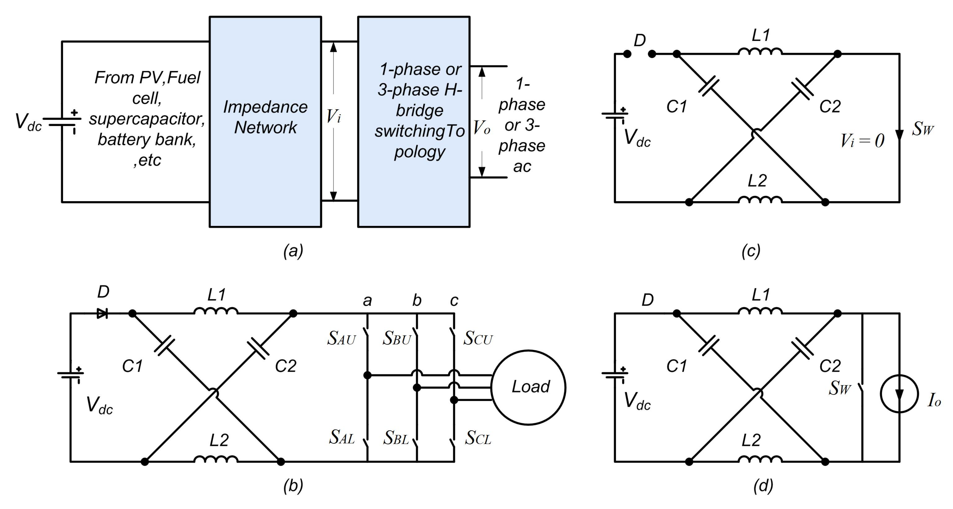
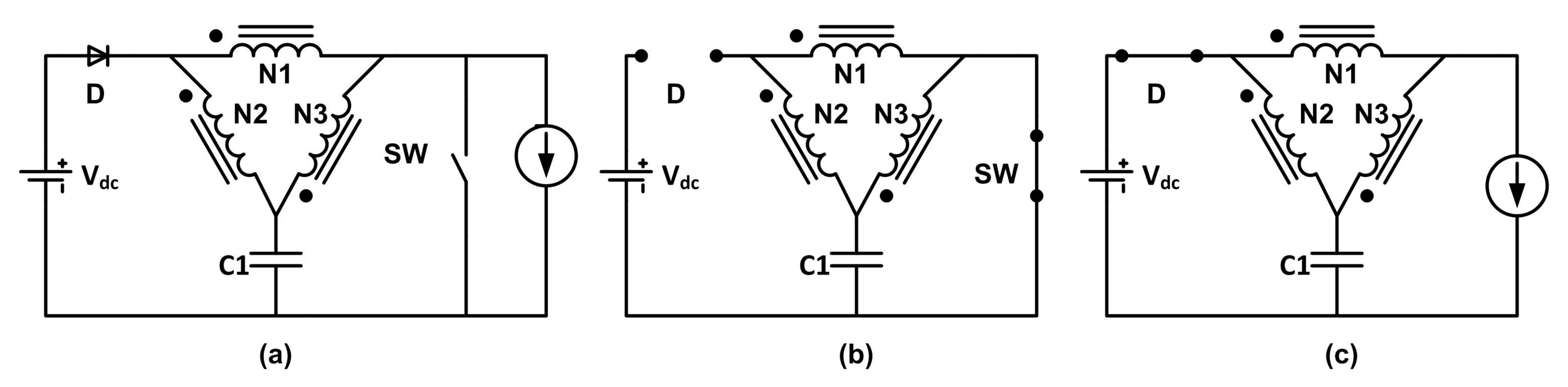
2. Operating Principle of Impedance Source Network

The operating principle depicting the high boosting feature of an impedance network is illustrated here by considering the basic Z-source configuration. The basic Z-source network is used to explain the functioning principle of the impedance network, which depicts the high voltage boost feature. An impedance source inverter (ZSI) is constitutes by an impedance network along with a voltage source inverter, which differs from a conventional VSI because of its high boosting capability. An impedance network consists of resistance, capacitors and inductors, whereas a VSI is made up of non-linear semiconductor switches. Shoot-through mode (Mode I) and non-shoot-through mode (Mode II) are the two basic operations describing the unconventional boost feature.

2.1. Mode I

The MCIS networks differ from VSI due to the shoot-through state. VSI legs are never short-circuited in normal operation, whereas the presence of an impedance network at the input of a VSI allows the short-circuiting of the upper and lower switches of a leg. This principle is utilized in all MCIS networks. A normal VSI operates in six active states and two zero states; however, an MCIS network will utilize all VSI states along with the shoot-through ( S T H ) zero state. The various shoot-through zero states are given in Table 1, where the upper and lower switches are short-circuited in different combinations. Conventional SPWM can generate the normal VSI states; however, different modulation controls can be utilized to generate S T H states [39,40,41,42,43,44]. Different circuit configurations of ZSI are shown in Figure 1. Unconventional boost is a distinguishing feature of ZSI, as it utilizes an extra zero state ( S T H ) and thus can operate with nine states. In this mode, the load is short-circuited, as indicated by switch S W ; diode ‘D’ is in an inactive state, and the passive elements of the impedance source network store energy, whereas the load receives no power, as shown in Figure 1.
Table 1. Shoot-through zero states for ZSI.
Switching StateConducting Switches
S T H 1 S A U , S A L
S T H 2 S B U , S B L
S T H 3 S C U , S C L
S T H 4 S A U , S A L , S B U , S B L
S T H 5 S A U , S A L , S C U , S C L
S T H 6 S B U , S B L , S C U , S C L
S T H 7 S A U , S A L , S B U , S B L , S C U , S C L

2.2. Mode II

As indicated in Figure 1, during Mode II, the diode ’D’ is active, whereas the load receives power from the source and inductor. With the discovery of this new shoot-through ( S T H ) state, ZSI demonstrates unexpected boosting in the presence of an impedance network. Various modulation techniques are available to integrate the S T H zero state with other conventional SPWM states [39,40,41,42,43,44].
During steady-state operation, the average voltage across the inductor will be ‘0’ for a switching period T s due to inductor volt-second balancing. The output voltage of the inverter is expressed by Equation (3), where V c 1 is the capacitor voltage, V ^ i is the inverter input peak voltage, V o is the phase peak, and M is the modulation index. Steady-state values are obtained as follows:
V c 1 = 1 D o 1 2 D o v d c = V c 2 + v d c
V ^ i = 1 1 2 D o v d c = V c 1 + V c 2
V o = M 2 V ^ i = 1 1 2 D o M 2 v d c = B M 2 v d c
The boost factor (B) for ZSI is given in Equation (3), where the output voltage of an inverter has two degrees of freedom, M and D o , as shown in Equation (3). Thus, V o can be controlled by modifying the control parameters M and d o , as d o = D o during the steady state.

3. Magnetically Coupled Impedance Source Network Topological Advancement

Magnetically coupled impedance source networks are different from conventional impedance source networks, as they use coupled winding or inductors. The major topologies reported use either two or three coupled winding components or inductors; they are different from each other in terms of the active and passive components used in the impedance network. MCIS networks are capable of high boost at low d s t , use a smaller number of components for the same features as non-transformer-based topologies and have high power density. This section presents a detailed comparison among various MCIS topologies; comparison is carried out on various factors, which will help researchers in identifying the suitable network topology for a specific application. Thus far, three-winding MCIS networks are more versatile than two-winding MCIS networks, as they give more design choices, and more combinations of control parameters ( d s t , M, turn ratio) are possible. They offer high power density with a low core size and thus improved efficiency. Later, it is shown that most of the two-winding topologies can be derived using three-winding MCIS networks.

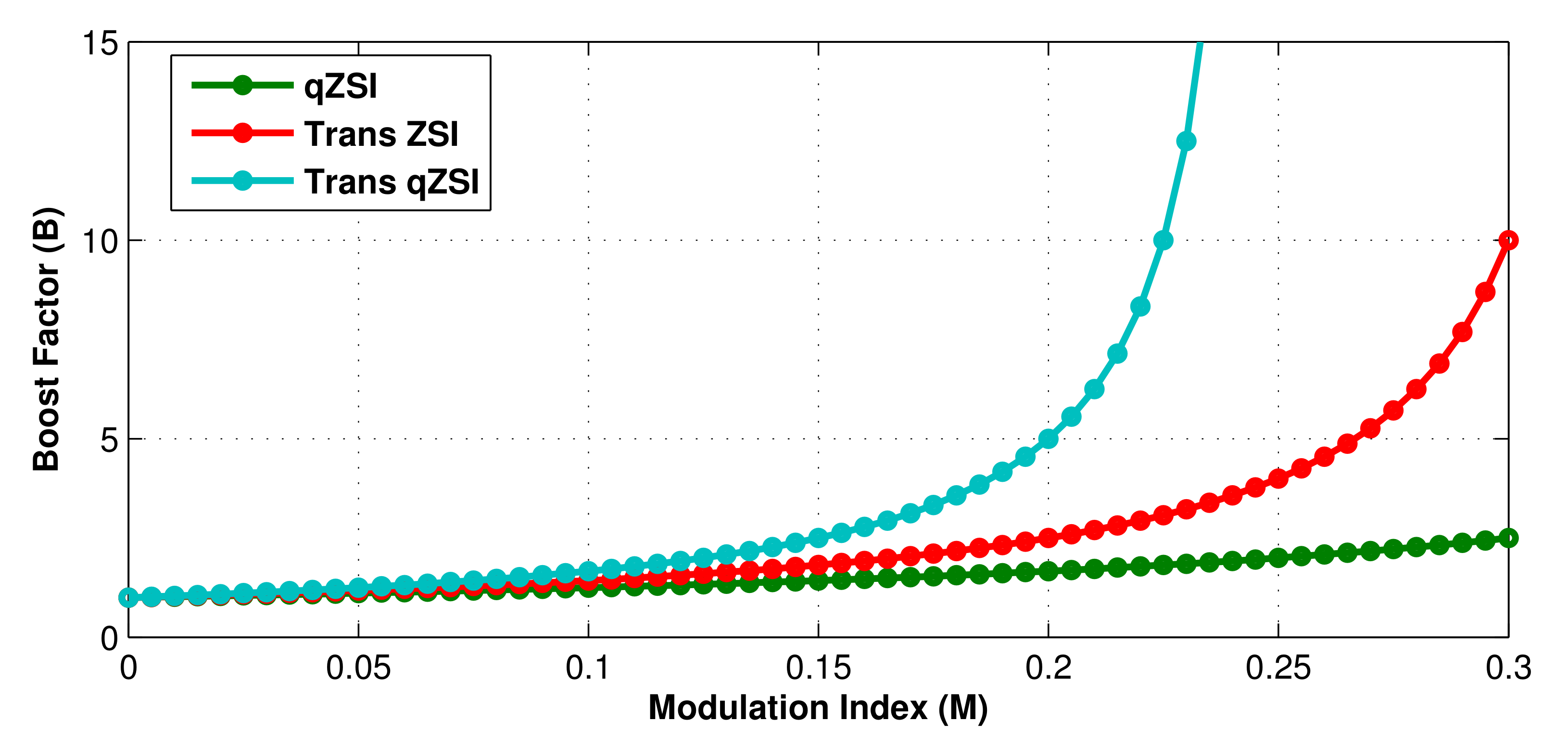
3.1. T-Source or Trans-Z-Source Impedance Network

Z-source/quasi Z-source networks have gained considerable attention in the last decade among many researchers, and have shown their utility in renewable energy generation. Both network types’ theoretical gain can be said to be infinite (∞), but practically, a high voltage boost will lead to a low modulation index, which in turn places more stress (voltage) on the components, thus offering limited boost capabilities. T-source and Trans-Z-source impedance networks are proposed in [37,45]; they are derived from the conventional ZSI/qZSI topologies, where the inductor pair is replaced by a magnetic core transformer with turn ratio N : 1 . They have higher boost capabilities. Various configurations of Trans-Z-source networks investigated so far are derived from current/voltage-fed Z source impedance or quasi-Z-source impedance networks. As per their origin, they are referred as voltage-fed trans-ZSI, voltage-fed trans-qZSI, current-fed trans-ZSI and current-fed trans-qZSI. A basic configuration of T-source or Trans-Z-source, trans-quasi-Z source and Trans-Z-source networks with an input filter is shown in Figure 3. In a voltage-fed trans-Z-source network, the current drawn from the source is discontinuous, as well as drawing a high inrush current, which can be improved using a front-end LC input filter. An improved trans-Z-source inverter is shown in Figure 4, which draws a continuous current from the source, suppresses the high starting inrush current and provides resonant current suppression. It consists of an additional inductance L3 and capacitance C2, as shown in the Figure 4; with the addition of two components, the voltage boost capabilities are better than trans-qZSI and trans-ZSI (or T-source). Hence, a high boost factor with lower voltage stress on components can be obtained with the same turn ratio; the detailed comparison is presented in Table 2.
MCIS topologies are characterized by a high voltage gain; as a result, voltage and current stress are also increased in the converter components; for a loose coupling, the problem is further exacerbated. Thus, to distribute the voltage and current stress, a cascaded trans-Z-source inverter topology is proposed [46]. In this topology, multiple coupled inductor cells with a lower number of turns are used to produce the same voltage gain. With lower turns, coupling is improved, and stress is reduced as compared to a basic topology. The major drawback compared to non-cascaded topologies is the increase in the number of components; therefore, it may be preferred in those applications that restrict the use of the high rating component, or where the use of a lower rating component is desirable. The effect of leakage inductance can reduce the voltage gain along with low output voltage quality; another topology is proposed [47] to counter leakage inductance, which uses two coupled transformers, two capacitors and two diodes. It produces higher voltage than the traditional trans-Z-source family. The efficiency is same as that of a TZ-source network, and higher than that of a cascaded multicell trans-Z-source network. Smaller capacitor voltage stress, lower voltage stresses of the diodes and a smaller SDP factor are the main advantages. Transformer leakage inductance is reduced by using bifilar winding design technology.
Table 2. Comparison of ZSI, qZSI, Trans-ZSI, Improved Trans-qZSI and Improved Trans-ZSI with two-transformer impedance network topology.
ZSI [20,48,49,50,51,52,53]qZSI [22,54,55,56,57,58,59,60,61,62]Trans-ZSI or T-ZSI [37,45,46]Trans-qZSI [63]Improved Trans-qZSI [64]Improved Trans-ZSI with two transformers [47]
Boost factor ( 1 2 d s t ) 1 ( 1 2 d s t ) 1 ( 1 ( 1 + N ) d s t ) 1 ( 1 ( 1 + N ) d s t ) 1 ( 1 ( 2 + N ) d s t ) 1 ( ( N t 2 + 1 ) d s t 2 ( N t 1 + N t 2 + 2 ) d s t + 1 ) 1
Component used
Capacitor221122
Inductor22--1-
Coupled Inductor--2222
Diode111112
Current drawn from sourcediscontinuouscontinuous, highly rippleddiscontinuouscontinuous, highly rippledcontinuousdiscontinuous
Draws inrush currentyesnoyesnonono
Commentfirst impedance source network, high voltage stress on componentsfirst modified ZSI, lower voltage stress for same voltage gain, reduced component ratinghigher gain, reduced component, LC i/p filter to suppress high inrush currentreduced component, LC i/p filter to suppress high ripples in input currenthighest gain, reduced component count (trans-ZSI/qZSI with LC i/p filter)higher voltage gain than trans-ZSI, cascaded multicell trans-ZSI and A-source network, lower voltage stress on diode and capacitors

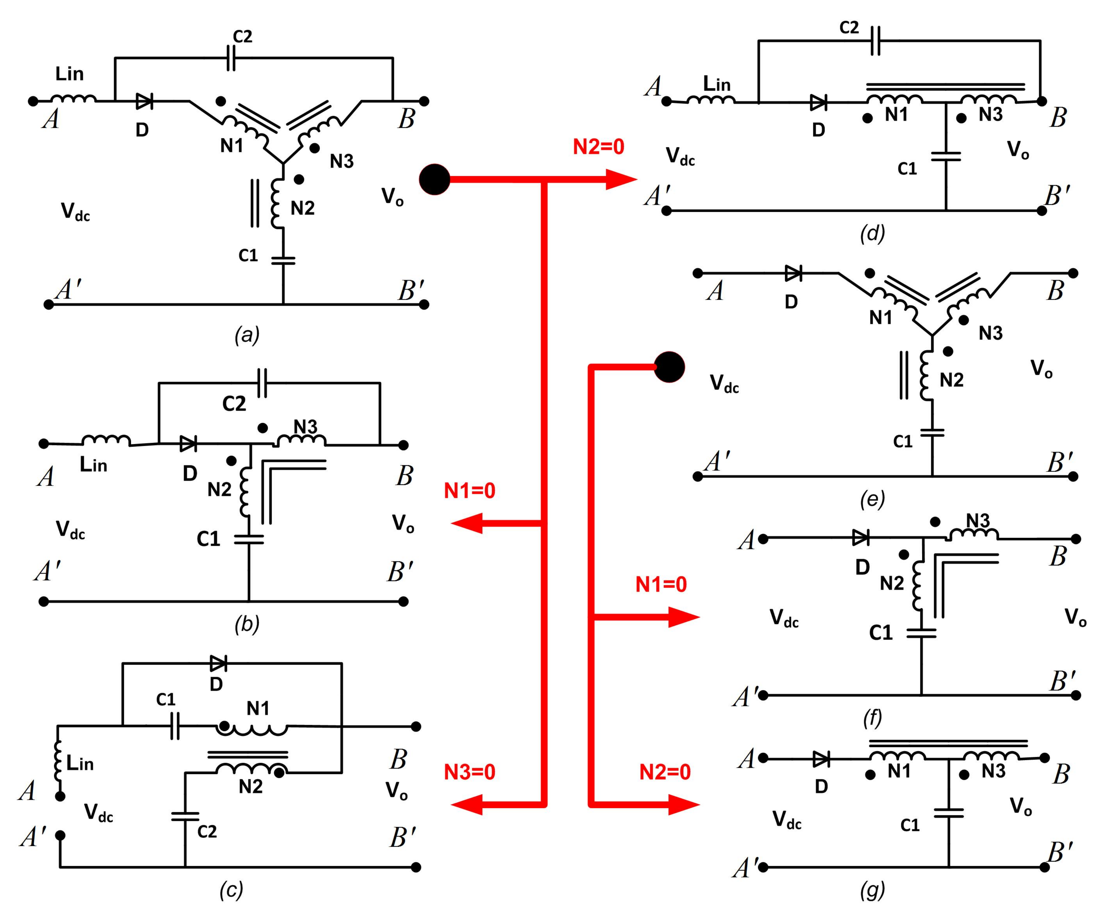
3.2. TZ-Source Impedance Network

When two inductors of a conventional Z-source network are replaced with two-transformer/coupled inductors, as shown in Figure 5, the resulting impedance network is referred to as a TZ-source impedance network [65]. It draws a discontinuous current and hence requires a front-end LC input filter such as Trans-Z source, so as to protect the energy source. It draws a starting inrush current, but the embedded quasi-TZ-source network topology is equipped with inherent inrush current suppression; this topology can be further extended to quasi or embedded ZSI topologies [65]. The distinguishing features of this topology are the higher boost gain than that of Trans-ZSI and LCCT networks. For the same voltage gain, it requires a lower turn ratio; as a result, the size of the transformer (power rating) and transformer core are reduced and thus the overall weight of the transformer is lower. However, the component count is higher when the front-end LC input filter is used to suppress the current and voltage spikes.
Boost factor variation for different modulation indexes is plotted for ZSI/qZSI, Trans-ZSI and Trans-qZSI for N = 2, as shown in Figure 6. Due to the presence of an additional control parameter (N) in the boost factor of the magnetically coupled impedance topology, a high voltage gain is visible in Figure 6.

3.3. LCCT Impedance Network

In this impedance network, out of two pairs of conventional LC networks (L1,C1 and L2,C2), one inductor (L2) and one capacitor (C1) are combined into a high-frequency transformer, as shown in Figure 7. Unlike Trans-Z source and TZ networks, it draws a continuous input current from the source, which is the prime requirement of most of the renewable energy applications. It has inherent dc blocking capabilities, due to the presence of two blocking capacitors; thus, transformer core saturation is also prevented. It has a reduced component count compared to previous topologies and offers a continuous current with high starting inrush current suppression. Variation in the boost factor with the shoot-through duty ratio is shown in Figure 8, where plots were obtained for different turn ratios k, where k = N.

3.4. Gamma Impedance Source Inverter ( Γ ZSI)

In all traditional MCIS (e.g., Trans-Z source, TZ source and LCCT network), a higher turn ratio is the prime requirement to obtain a higher voltage gain, which sometimes may not be practically realizable. However, unlike traditional MCIS, a higher voltage gain is obtained by lowering the turn ratio in the case of Γ ZSI, which is a unique feature of this new topology [66]. With a different placement of the coupled inductor, a very high voltage gain along with a lower component count is realizable in the Γ Z source network topology shown in Figure 9. However, it draws a discontinuous current from the source. Variation in the boost factor with the shoot-through duty ratio is shown in Figure 8, where plots were obtained for different turn ratios k, where k = 1 N Γ Z . The voltage boost for Trans-Z source and Γ Z source matches for N T Z = 1 N Γ Z 1 .
With a slight modification in the Γ Z source network, the current drawn from the source can be made continuous. An improved or modified Γ Z source network is also referred to as an asymmetrical Γ Z source network. It uses an additional inductor Lin and capacitor C2 when compared with its counterpart; an additional input inductor will reduce the current spike during starting and also helps in smoothing the input current. Lowering the turn ratio will lead to a higher voltage gain in this modified Γ Z network, as with its counterpart, but it draws a continuous current. Variation in the boost factor with the shoot-through duty ratio for an asymmetrical Γ Z-source network is shown in Figure 8; plots are obtained for different turn ratios k, where k = 1 N Γ Z . The voltage boost for Trans-Z source and asymmetrical Γ Z source matches for N T Z = 1 + 1 N Γ Z 1 .
The sigma (∑) source network is proposed in [67] by reconfiguring the TZ-source network, which uses two transformers whose secondary windings are connected to capacitors. It can be viewed as a dual Γ Z source network, forming a sigma (∑) source network, and is known as the ∑-ZSI topology. When compared to the TZ-source network, it uses the same number of components, but high voltage gain is possible at a lower turn ratio. Thus, the size of the two transformers will be smaller, and the modulation index will be higher due to the lower duty cycle ( d s t ); hence, there is low voltage stress on the components for the same voltage gain.

3.5. Y-Source Impedance Network

All the above topologies use a two-winding coupled transformer and are better than conventional ZSI in terms of higher voltage gain and some have even lower component counts. With certain improvements, a further higher voltage gain is possible with reduced d s t and a high modulation index (M). As a result, there will be less voltage stress on components due to high (M), but at the cost of a higher component count. A Y-source impedance network consisting of three coupled winding ( N 1 , N 2 , N 3 ) is proposed in [68]. As shown in Figure 10, its gain capability is the highest for the same shoot-through duty cycle ( d s t ) among all the above topologies. For a narrower d s t , a higher modulation index (M) is possible; as a result, voltage stress on components is the lowest with the same gain compared with its counterparts. The desired gain can be obtained by various combinations of d s t and k, where k is an additional degree of freedom ( k = N 3 N 1 N 3 N 2 ); thus, more design choices are possible in the case of Y-source.
Y-source has merged all the merits of the above two-winding MCIS topologies. It can be characterized by a very high voltage gain with tight coupling, a lower component count, low voltage stress for the same gain, reduced component rating and more design choices. However, it draws a discontinuous current from the source, and high inrush current during starting. With a small modification, Y-source networks can draw a continuous input current, as done in previous topologies. The improved Y-source impedance network is shown in Figure 10; they can be classified as improved Y-source type I and type II. In type I, a smoothing inductor and capacitor is added in the original Y-source network. Compared to the original network, it draws a continuous current, and high gain is obtained at the same d s t , with high voltage stress on components. In a type II network, the input current is continuous for certain capacitance ratios between C1 and C2, but it can affect the performance greatly if the capacitance ratio is not accurately set. The risks of high inrush current at startup and input oscillations due to parasitic inductances and capacitances persist. Variation in the boost factor with the shoot-through duty ratio for Y-source and improved Y-source is shown in Figure 11; plots are obtained for different turn ratios.
A quasi-Y-source impedance network is proposed in [69]; it retains the original Y-source network configuration, i.e., three coupled winding ( N 1 , N 2 , N 3 ) and capacitor C1 in their original position. An additional input inductor and dc blocking capacitor are used (Lin and C2), and the position of the diode (D) is changed, as shown in Figure 10. The winding factor ( δ = N 1 + N 2 N 2 N 3 ) of the quasi-Y-source network is different from that of the original Y-source network; however, it will have the same voltage gain as long as both winding factors are equal ( δ = k ). Both the Y-source and quasi-Y source networks must satisfy the inequalities [ 1 < N 3 , N 3 > N 2 ] and [ 1 < N 2 , N 2 > N 3 ] , respectively, for satisfactory performance. The quasi-Y-source network draws a continuous current, prevents core saturation due to the presence of dc blocking capacitor C2 and there is no startup inrush current. It has a low component count and a reduced core size of the transformer for the same voltage gain, hence offering the best characteristics at a certain capacitance ratio ( C 1 C 2 = δ 1 ), maintained when compared with previous MCIS topologies. Most of the two-winding topologies can be derived from Y-source impedance networks, as shown in Figure 12; thus, the Y-source topology has merged all the merits of the two-winding topology.

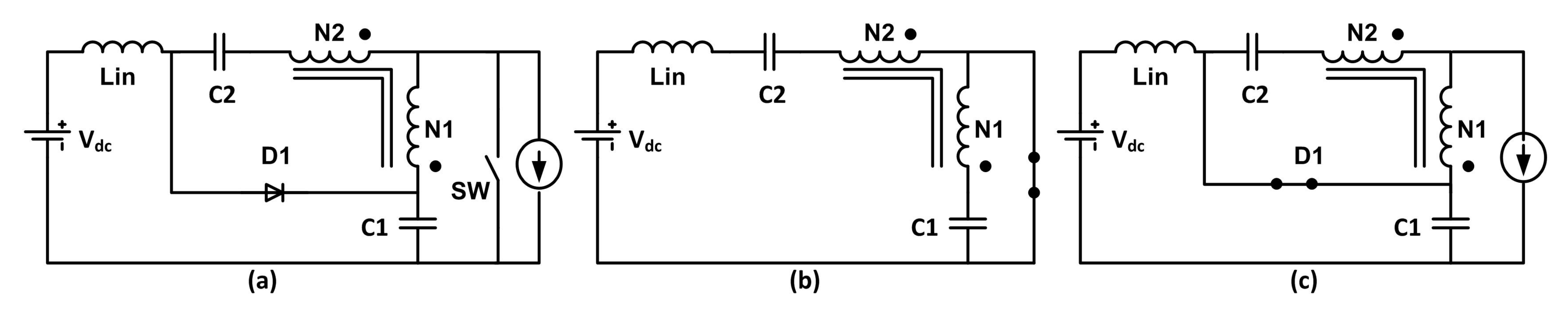
3.6. Coupled Inductor L-Source Inverter (CL-LSI)

It is composed of a switch with an antiparallel diode in series with a capacitor, and a coupled inductor forming an L-shaped impedance network, as shown in Figure 13. The main feature of this impedance network is that it can work in continious conduction mode (CCM) as well as in discontinuous conduction mode (DCM); hence, it can solve the problem of dc link voltage drop. Compared to CCM, in DCM, it produces a higher voltage gain with lower voltage stress on components. It also has a reduced size of the coupled inductor along with low power loss, and suppresses the startup inrush current [70].

3.7. A-Source Impedance Network

This impedance network is a two-winding MCIS network, consisting of a smoothing inductor L i n , a diode D1, capacitors C1 and C2 and an autotransformer. This autotransformer has L 1 , N 1 and L 2 , N 2 as the primary and secondary winding inductances and turns, respectively, as shown in Figure 14. Higher voltage gain is obtained by using an autotransformer-type wound coupled inductor instead of a normal wound coupled inductor. To have small leakage inductance, tight coupling is ensured. It provides higher voltage gain with a lower turn ratio; as a result, the weight and size of the coupled inductor are reduced, with higher power density, when compared with Z-source, Trans-Z-source, LCCT-Z-source, Γ Z source and Y-source. It draws a continuous current from the source, and the variation in the boost factor with the shoot-through duty ratio is shown in Figure 8. Plots are obtained for different turn ratios k, where k = N 2 N 1 .

3.8. Δ -Source Impedance Network

The proposed impedance network uses the same components as that of Y-source, and is also a three-winding MCIS network topology. It only differs in the layout of the three windings, forming a Δ shape, as shown in Figure 15. All magnetically coupled impedance networks’ performance is sensitive to leakage inductance; as a result, precise closed loop control will lead to additional costs and complexity. The Δ -source impedance network offers smaller leakage inductance compared to its counterpart Y-source network. It also draws a smaller magnetizing current and has lower power losses. The desired voltage gain can be obtained by various combinations of d s t and k Δ , where k Δ is an additional degree of freedom ( k Δ = N 1 N 3 ). The main advantage of this topology over Y-source is the reduced leakage current; thus, the size and volume of the three-winding transformer are also reduced for the same voltage gain, which leads to lower winding losses and hence a high output voltage with the same boosting. However, it has a drawback of higher magnetizing current ripple; as a result, there are higher core losses compared with Y-source, and it draws a discontinuous current from the source and high inrush current during starting.
The performance of MCIS networks is remarkable in terms of boost capability; the results obtained are described and measured considering ideal conditions. However, the acclaimed performance deteriorates, largely due to the effect of the parasitic resistance of the impedance network. The overall gain is highly affected by the parasitic resistances of the impedance network and switching devices. The mathematically derived results from circuit modeling and circuit analysis directly relate the overall voltage gain to the parasitic resistance, which can be further investigated for other scenarios. In summary, the parasitic resistance will decrease the overall voltage gain; however, the severity of the gain drop can be further investigated with different shoot-through duty ratios, different resistance ratios and different winding ratios. The work on MCIS topologies can now be directed towards new horizons, such as analysis for the effect of leakage inductance and parasitic resistance on overall gain. Shoot-through duty ratio constraints can also be explored for the implementation of closed loop control applications. All two-winding, three-winding and autotransformer-based MCIS topologies should be further explored to minimize the effect of zero right half plane (RHP) on control-related performance.

4. Conclusions

Magnetically coupled impedance source networks have seen rapid advancements in the last few years; they have proven their superiority in efficient power conversion compared to any other two-stage or single-stage converter topologies, as they overcome most of the problems associated with traditional converter topologies. Since the first reported MCIS network (T-Source), there has been a rapid evolution in new MCIS topologies as well as improved or modified MCIS topologies; this niche area has attracted many researchers and designers for further exploration. The existing reported MCIS networks are better in terms of high output voltage, lower voltage and current stress on components. They have a lower component count for the same features, draw a continuous current from the source and experience low startup inrush current. This paper does not aim to advocate for any specific topology, but presents a comparative analysis and a comprehensive review of various advancements in MCIS networks since their inception, and best efforts are made to include all relevant contributions of all researchers and designers. A close study revealed that some of the driving factors for major modifications are: (1) to have a high boosting factor (B); (2) to have more degrees of freedom; (3) to achieve high boost at low d s t so as to best utilize the source voltage; (4) to reduce the component count; (5) to reduce the voltage stress on components; (6) to draw continuous input current from the source; (7) to draw low startup inrush current with less ripples; (8) dc blocking so as to avoid core saturation; (9) to have a reduced core size, increased power density and efficiency, etc. The common problem faced by all MCIS topologies is leakage inductance; tight coupling of the coupled winding is necessary to achieve the acclaimed performance, and it can be achieved by using bifilar winding design technology.
MCIS network topologies have found application in various types of ac-dc, dc-dc, dc-ac, ac-ac unidirectional or bi-directional power conversion. Table 2 shows a detailed comparison between ZSI, Trans-ZSI or T-ZSI, Trans-qZSI, Improved Trans-qZSI and Improved Trans-ZSI with two transformers; Table 3 shows a detailed comparison between LCCT-Z Source, Γ -Source, Asym- Γ -Source, Σ -Source and A-Source, whereas Table 4 shows a detailed comparison between Y-Source, Improved Y-source, Quasi-Y Source and Δ -Source. The various topologies are different from each other in terms of their impedance network configuration, which makes their characteristics unique. However, it is impossible to suggest one topology for various application(s), as some topologies can find a niche over other topologies in some application(s); therefore, this paper can help researchers to compare the different MCIS network topologies, to categorize them according to various comparative factors presented in Table 2, Table 3 and Table 4 and to choose the appropriate MCIS network for their application.
Table 3. Comparison of LCCT-Z Source, Γ -Source, Asym- Γ -Source, Σ -Source and A-Source impedance networks.
LCCT-Z Source [71,72,73] Γ -Source [66,74]Asym- Γ -Source [75] Σ -Source [67]A-Source [76]
Boost factor ( 1 ( N + 1 ) d s t ) 1 ( 1 ( 1 + ( 1 N Γ Z 1 ) ) d s t ) 1 ( 1 ( 2 + ( 1 N Γ Z 1 ) ) d s t ) 1 ( 1 ( 2 + 1 N Γ 1 1 + 1 N Γ 2 1 ) d s t ) 1 ( 1 ( 2 + N 2 N 1 ) d s t ) 1
Component used
Capacitor21222
Inductor1-1-1
Coupled Inductor11121
Diode11111
Current drawn from sourcecontinuousdiscontinuouscontinuousdiscontinuouscontinuous
Draws inrush currentnoyesnoyesno
Commentinherent dc blocking, continuous current even at light loadhigh gain by lowering turn ratio, reduced core size, less componenthigh gain by lowering turn ratio, suppresses high inrush current, reduced core sizehigh gain, low voltage stress, reduced core sizeuses autotransformer, reduced turn ratio for same gain, high power density
Table 4. Comparison of three-winding magnetically coupled impedance source (MCIS) networks.
Y-Source [68,69,77]Improved Y-Source [69,78,79]Quasi-Y Source [69,78,79] Δ -Source [80]
Type IType II
Boost factor ( 1 k d s t ) 1 ( 1 ( 1 + k ) d s t ) 1 ( 1 k d s t ) 1 ( 1 δ d s t ) 1 ( 1 k Δ d s t ) 1
Component used
Capacitor12221
Inductor-1-1-
Three-winding coupled inductor11111
Diode11111
Current drawn from sourcediscontinuouscontinuouscontinuouscontinuousdiscontinuous
Draws inrush currentyes yesnoyes
Commenthas 3 degree of freedom, more design choices, very high boost at low d s t compared to two winding MCIS topology, versatilesmoothing inductor and capacitor is added, high voltage gain at same d s t , high voltage stress, improved performance at the cost of high component countcertain C 1 C 2 ratio is maintained for continuous current, risk of high inrush current and high startup inrush current, sensitive to capacitor ESR and parameter variationsame gain for  δ = k , inherent dc blocking, reduced core size for same voltage gainlower magnetizing current, high output voltage at same B compared to original Y-source but high core losses due to highly rippled magnetizing current

Author Contributions

Conceptualization, A.Y., S.C. and M.B.; methodology, A.Y. and S.C.; validation, A.Y., S.C., M.B. and E.M.A.; formal analysis, A.Y. and S.K.; investigation, A.Y.; resources, A.Y., M.B. and E.M.A.; writing—original draft preparation, A.Y.; writing—review and editing, A.Y., S.C., M.B., N.K.S., E.M.A. and S.K.; visualization, A.Y. and S.C.; final version writing—review, editing, and funding A.Y. and E.M.A. All authors have read and agreed to the published version of the manuscript.

Funding

This work was funded by the Deanship of Scientific Research at Jouf University under grant No (DSR-2021-02-0310).

Institutional Review Board Statement

Not applicable.

Informed Consent Statement

Not applicable.

Data Availability Statement

The data that support the findings of this study are available from the corresponding author upon reasonable request.

Acknowledgments

The authors acknowledge the financial support received from the Jouf University Researchers’ under grant No (DSR-2021-02-0310), Jouf University, Sakaka, Saudi Arabia. In addition, the authors would like to thank GLA University, Mathura, India, for their support in obtaining all our research publications and outputs.

Conflicts of Interest

The authors declare no conflict of interest.

References

  1. Xue, Y.; Chang, L.; Kjaer, S.B.; Bordonau, J.; Shimizu, T. Topologies of single-phase inverters for small distributed power generators: An overview. IEEE Trans. Power Electron. 2004, 19, 1305–1314. [Google Scholar] [CrossRef]
  2. Kjaer, S.B.; Pedersen, J.K.; Blaabjerg, F. Power inverter topologies for photovoltaic modules-a review. In Proceedings of the 37th IAS Annual Meeting (Cat. No. 02CH37344), Pittsburgh, PA, USA, 13–18 October 2002; Volume 2, pp. 782–788. [Google Scholar]
  3. Jain, S.; Agarwal, V. A single-stage grid connected inverter topology for solar PV systems with maximum power point tracking. IEEE Trans. Power Electron. 2007, 22, 1928–1940. [Google Scholar] [CrossRef] [Green Version]
  4. Kjaer, S.B.; Pedersen, J.K.; Blaabjerg, F. A review of single-phase grid-connected inverters for photovoltaic modules. IEEE Trans. Ind. Appl. 2005, 41, 1292–1306. [Google Scholar] [CrossRef]
  5. Li, Q.; Wolfs, P. A review of the single phase photovoltaic module integrated converter topologies with three different DC link configurations. IEEE Trans. Power Electron. 2008, 23, 1320–1333. [Google Scholar]
  6. Araújo, S.V.; Zacharias, P.; Mallwitz, R. Highly efficient single-phase transformerless inverters for grid-connected photovoltaic systems. IEEE Trans. Ind. Electron. 2010, 57, 3118–3128. [Google Scholar] [CrossRef]
  7. Rodriguez, J.; Lai, J.S.; Peng, F.Z. Multilevel inverters: A survey of topologies, controls, and applications. IEEE Trans. Ind. Electron. 2002, 49, 724–738. [Google Scholar] [CrossRef] [Green Version]
  8. Daher, S.; Schmid, J.; Antunes, F.L. Multilevel inverter topologies for stand-alone PV systems. IEEE Trans. Ind. Electron. 2008, 55, 2703–2712. [Google Scholar] [CrossRef]
  9. Gupta, K.K.; Ranjan, A.; Bhatnagar, P.; Sahu, L.K.; Jain, S. Multilevel inverter topologies with reduced device count: A review. IEEE Trans. Power Electron. 2016, 31, 135–151. [Google Scholar] [CrossRef]
  10. Peng, F.Z. A generalized multilevel inverter topology with self voltage balancing. In Proceedings of the Conference Record of the 2000 Industry Applications Conference, Rome, Italy, 8–12 October 2000; Volume 3, pp. 2024–2031. [Google Scholar]
  11. Gupta, H.; Yadav, A.; Maurya, S. Dynamic performance of cascade multilevel inverter based STATCOM. In Proceedings of the Power Electronics, Intelligent Control and Energy Systems (ICPEICES), New Delhi, India, 4–6 July 2016; pp. 1–4. [Google Scholar]
  12. Gupta, H.; Yadav, A.; Maurya, S. Multi carrier PWM and selective harmonic elimination technique for cascade multilevel inverter. In Proceedings of the Advances in Electrical, Electronics, Information, Communication and Bio-Informatics (AEEICB), Chennai, India, 27–28 February 2016; pp. 98–102. [Google Scholar]
  13. Loh, P.C.; Vilathgamuwa, D.M.; Gajanayake, C.J.; Lim, Y.R.; Teo, C.W. Transient modeling and analysis of pulse-width modulated Z-source inverter. IEEE Trans. Power Electron. 2007, 22, 498–507. [Google Scholar] [CrossRef]
  14. Shen, M.; Peng, F.Z. Operation modes and characteristics of the Z-source inverter with small inductance or low power factor. IEEE Trans. Ind. Electron. 2008, 55, 89–96. [Google Scholar] [CrossRef]
  15. Li, Y.; Anderson, J.; Peng, F.Z.; Liu, D. Quasi-Z-source inverter for photovoltaic power generation systems. In Proceedings of the 2009 Twenty-Fourth Annual IEEE Applied Power Electronics Conference and Exposition, APEC 2009, Washington, DC, USA, 15–19 February 2009; pp. 918–924. [Google Scholar]
  16. Tang, Y.; Xie, S.; Zhang, C.; Xu, Z. Improved Z-source inverter with reduced Z-source capacitor voltage stress and soft-start capability. IEEE Trans. Power Electron. 2009, 24, 409–415. [Google Scholar] [CrossRef]
  17. Huang, Y.; Shen, M.; Peng, F.Z.; Wang, J. Z-Source Inverter for Residential Photovoltaic Systems. IEEE Trans. Power Electron. 2006, 21, 1776–1782. [Google Scholar] [CrossRef]
  18. Tang, Y.; Xie, S.; Zhang, C. An improved Z-source inverter. IEEE Trans. Power Electron. 2011, 26, 3865–3868. [Google Scholar] [CrossRef]
  19. Yang, S.; Peng, F.Z.; Lei, Q.; Inoshita, R.; Qian, Z. Current-fed quasi-Z-source inverter with voltage buck–boost and regeneration capability. IEEE Trans. Ind. Appl. 2011, 47, 882–892. [Google Scholar] [CrossRef]
  20. Peng, F.Z. Z-source inverter. IEEE Trans. Ind. Appl. 2003, 39, 504–510. [Google Scholar] [CrossRef]
  21. Peng, F.Z.; Joseph, A.; Wang, J.; Shen, M.; Chen, L.; Pan, Z.; Ortiz-Rivera, E.; Huang, Y. Z-source inverter for motor drives. IEEE Trans. Power Electron. 2005, 20, 857–863. [Google Scholar] [CrossRef]
  22. Li, Y.; Jiang, S.; Cintron-Rivera, J.G.; Peng, F.Z. Modeling and control of quasi-Z-source inverter for distributed generation applications. IEEE Trans. Ind. Electron. 2013, 60, 1532–1541. [Google Scholar] [CrossRef]
  23. Jammy, R.R.; Annamalai, K. A new configuration of seven-level quasi Z-source–based isolated inverter for renewable applications. Int. Trans. Electr. Energy Syst. 2019, 29, e2833. [Google Scholar] [CrossRef]
  24. Zhou, Z.J.; Zhang, X.; Xu, P.; Shen, W.X. Single-phase uninterruptible power supply based on Z-source inverter. IEEE Trans. Ind. Electron. 2008, 55, 2997–3004. [Google Scholar] [CrossRef]
  25. Peng, F.Z.; Shen, M.; Holland, K. Application of Z-source inverter for traction drive of fuel cell—Battery hybrid electric vehicles. IEEE Trans. Power Electron. 2007, 22, 1054–1061. [Google Scholar] [CrossRef]
  26. Shen, M.; Joseph, A.; Wang, J.; Peng, F.Z.; Adams, D.J. Comparison of traditional inverters and Z-source inverter for fuel cell vehicles. IEEE Trans. Power Electron. 2007, 22, 1453–1463. [Google Scholar] [CrossRef]
  27. Hanif, M.; Basu, M.; Gaughan, K. Understanding the operation of a Z-source inverter for photovoltaic application with a design example. IET Power Electron. 2011, 4, 278–287. [Google Scholar] [CrossRef]
  28. Yadav, A.; Deolia, V.K.; Agrawal, S. Indirect closed loop control of quasi-Z-source inverter for standalone solar PV-based energy conversion system. Int. J. Power Energy Convers. 2021, 12, 236–251. [Google Scholar] [CrossRef]
  29. Yadav, A.; Deolia, V.K.; Agrawal, S. Dual Current Loop Control for a Third-Order Passive Damped Filter Based Quasi-Z-Source Inverter. ECTI Trans. Electr. Eng. Electron. Commun. 2021, 19, 12–22. [Google Scholar] [CrossRef]
  30. Ellabban, O.; Abu-Rub, H. Z-source inverter: Topology improvements review. IEEE Ind. Electron. Mag. 2016, 10, 6–24. [Google Scholar] [CrossRef]
  31. Siwakoti, Y.P.; Peng, F.Z.; Blaabjerg, F.; Loh, P.C.; Town, G.E. Impedance-source networks for electric power conversion part I: A topological review. IEEE Trans. Power Electron. 2014, 30, 699–716. [Google Scholar] [CrossRef]
  32. Abdelhakim, A.; Blaabjerg, F.; Mattavelli, P. Modulation schemes of the three-phase impedance source inverters—Part I: Classification and review. IEEE Trans. Ind. Electron. 2018, 65, 6309–6320. [Google Scholar] [CrossRef]
  33. Abdelhakim, A.; Blaabjerg, F.; Mattavelli, P. Modulation schemes of the three-phase impedance source inverters—Part II: Comparative assessment. IEEE Trans. Ind. Electron. 2018, 65, 6321–6332. [Google Scholar] [CrossRef]
  34. Siwakoti, Y.P.; Peng, F.Z.; Blaabjerg, F.; Loh, P.C.; Town, G.E.; Yang, S. Impedance-source networks for electric power conversion part II: Review of control and modulation techniques. IEEE Trans. Power Electron. 2014, 30, 1887–1906. [Google Scholar] [CrossRef]
  35. Yadav, A.; Deolia, V.; Agrawal, S. Influence of parasitic resistance on dynamic response of a Quasi-Z-Source connected system. In Proceedings of the 2020 International Conference on Power Electronics & IOT Applications in Renewable Energy and Its Control (PARC), Mathura, UP, India, 28–29 February 2020; pp. 220–225. [Google Scholar] [CrossRef]
  36. Yadav, A.; Chandra, S. Single stage high boost Quasi-Z-Source inverter for off-grid photovoltaic application. In Proceedings of the 2020 International Conference on Power Electronics & IOT Applications in Renewable Energy and its Control (PARC), Mathura, UP, India, 28–29 February 2020; pp. 257–262. [Google Scholar] [CrossRef]
  37. Strzelecki, R.; Adamowicz, M.; Strzelecka, N.; Bury, W. New type T-source inverter. In Compatibility and Power Electronics; IEEE: Piscataway, NJ, USA, 2009; pp. 191–195. [Google Scholar]
  38. Liu, H.; Ji, Y.; Wang, L.; Wheeler, P. A family of improved magnetically coupled impedance network boost DC–DC converters. IEEE Trans. Power Electron. 2017, 33, 3697–3702. [Google Scholar] [CrossRef]
  39. Shen, M.; Wang, J.; Joseph, A.; Peng, F.Z.; Tolbert, L.M.; Adams, D.J. Constant boost control of the Z-source inverter to minimize current ripple and voltage stress. IEEE Trans. Ind. Appl. 2006, 42, 770–778. [Google Scholar] [CrossRef]
  40. Peng, F.Z.; Shen, M.; Qian, Z. Maximum boost control of the Z-source inverter. IEEE Trans. Power Electron. 2005, 20, 833–838. [Google Scholar] [CrossRef]
  41. Shen, M.; Wang, J.; Joseph, A.; Peng, F.Z.; Tolbert, L.M.; Adams, D.J. Maximum constant boost control of the Z-source inverter. In Proceedings of the 39th IAS Annual Meeting Industry Applications Conference, Edmonton, AB, Canada, 5–9 October 2004; Volume 1. [Google Scholar]
  42. Loh, P.C.; Vilathgamuwa, D.M.; Lai, Y.S.; Chua, G.T.; Li, Y. Pulse-width modulation of Z-source inverters. In Proceedings of the 2004 39th IAS Annual Meeting Industry Applications Conference, Washinghton, DC, USA, 3–7 October 2004; Volume 1. [Google Scholar]
  43. Ellabban, O.; Van Mierlo, J.; Lataire, P. Comparison between different PWM control methods for different Z-source inverter topologies. In Proceedings of the 2009 Power Electronics and Applications, EPE’09, Barcelona, Spain, 8–10 September 2009; pp. 1–11. [Google Scholar]
  44. Yadav, A.; Chandra, S.; Deolia, V.; Agrawal, S. Z source inverter application and control for decentralized photovoltaic system. In Proceedings of the Condition Assessment Techniques in Electrical Systems (CATCON), Chennai, India, 21–23 November 2017; pp. 52–57. [Google Scholar]
  45. Qian, W.; Peng, F.Z.; Cha, H. Trans-Z-source inverters. IEEE Trans. Power Electron. 2011, 26, 3453–3463. [Google Scholar] [CrossRef]
  46. Li, D.; Loh, P.C.; Zhu, M.; Gao, F.; Blaabjerg, F. Cascaded multicell trans-Z-source inverters. IEEE Trans. Power Electron. 2013, 28, 826–836. [Google Scholar]
  47. Kojabadi, H.M.; Kivi, H.F.; Blaabjerg, F. Experimental and theoretical analysis of trans-Z-source inverters with leakage inductance effects. IEEE Trans. Ind. Electron. 2018, 65, 977–987. [Google Scholar] [CrossRef]
  48. Tran, Q.V.; Chun, T.W.; Ahn, J.R.; Lee, H.H. Algorithms for controlling both the DC boost and AC output voltage of Z-source inverter. IEEE Trans. Ind. Electron. 2007, 54, 2745–2750. [Google Scholar] [CrossRef]
  49. Gajanayake, C.J.; Vilathgamuwa, D.M.; Loh, P.C. Development of a Comprehensive Model and a Multiloop Controller for Z-Source Inverter DG Systems. IEEE Trans. Ind. Electron. 2007, 54, 2352–2359. [Google Scholar] [CrossRef]
  50. Hakeem, A.A.; Elserougi, A.; El Zawawi, A.; Ahmed, S.; Massoud, A. A modified modulation scheme for capacitor voltage control of renewable energy-fed grid-connected z-source inverters. In Proceedings of the IECON 2012-38th Annual Conference on IEEE Industrial Electronics Society, Montreal, QC, Canada, 25–28 October 2012; pp. 886–893. [Google Scholar]
  51. Cavalcanti, M.; Bradaschia, F.; de Melo Neto, M.; Azevedo, G.; Cardoso, T. Dynamic modeling and control system design of the buck-boost-based three-state three-phase Z-source inverter. Int. J. Electr. Power Energy Syst. 2019, 104, 654–663. [Google Scholar] [CrossRef]
  52. Dehghanzadeh, A.R.; Behjat, V.; Banaei, M.R. Double input Z-source inverter applicable in dual-star PMSG based wind turbine. Int. J. Electr. Power Energy Syst. 2016, 82, 49–57. [Google Scholar] [CrossRef]
  53. Sonar, S.; Maity, T.; Minu, M. Single phase transformerless wide range ac boost voltage regulator based on z-source network. Int. J. Electr. Power Energy Syst. 2013, 47, 193–197. [Google Scholar] [CrossRef]
  54. Liu, Y.; Ge, B.; Abu-Rub, H.; Peng, F.Z. Control system design of battery-assisted quasi-Z-source inverter for grid-tie photovoltaic power generation. IEEE Trans. Sustain. Energy 2013, 4, 994–1001. [Google Scholar] [CrossRef]
  55. Ge, B.; Abu-Rub, H.; Peng, F.Z.; Lei, Q.; De Almeida, A.T.; Ferreira, F.J.; Sun, D.; Liu, Y. An energy-stored quasi-Z-source inverter for application to photovoltaic power system. IEEE Trans. Ind. Electron. 2013, 60, 4468–4481. [Google Scholar] [CrossRef]
  56. Abu-Rub, H.; Iqbal, A.; Ahmed, S.M.; Peng, F.Z.; Li, Y.; Baoming, G. Quasi-Z-source inverter-based photovoltaic generation system with maximum power tracking control using ANFIS. IEEE Trans. Sustain. Energy 2013, 4, 11–20. [Google Scholar] [CrossRef]
  57. Liu, Y.; Abu-Rub, H.; Ge, B. Z-Source∖/Quasi-Z-Source Inverters: Derived Networks, Modulations, Controls, and Emerging Applications to Photovoltaic Conversion. IEEE Ind. Electron. Mag. 2014, 8, 32–44. [Google Scholar] [CrossRef]
  58. Florez-Tapia, A.M.; Vadillo, J.; Martin-Villate, A.; Echeverria, J.M. Transient analysis of a trans quasi-Z-source inverter working in discontinuous conduction mode. Electr. Power Syst. Res. 2017, 151, 106–114. [Google Scholar] [CrossRef]
  59. Florez-Tapia, A.M.; Ibanez, F.M.; Vadillo, J.; Elosegui, I.; Echeverria, J.M. Small signal modeling and transient analysis of a Trans quasi-Z-source inverter. Electr. Power Syst. Res. 2017, 144, 52–62. [Google Scholar] [CrossRef]
  60. Rajasegharan, V.; Premalatha, L.; Rengaraj, R. Modelling and controlling of PV connected quasi Z-source cascaded multilevel inverter system: An HACSNN based control approach. Electr. Power Syst. Res. 2018, 162, 10–22. [Google Scholar]
  61. Khajesalehi, J.; Hamzeh, M.; Sheshyekani, K.; Afjei, E. Modeling and control of quasi Z-source inverters for parallel operation of battery energy storage systems: Application to microgrids. Electr. Power Syst. Res. 2015, 125, 164–173. [Google Scholar] [CrossRef]
  62. Sun, D.; Ge, B.; Bi, D.; Peng, F.Z. Analysis and control of quasi-Z source inverter with battery for grid-connected PV system. Int. J. Electr. Power Energy Syst. 2013, 46, 234–240. [Google Scholar] [CrossRef]
  63. Florez-Tapia, A.M.; Vadillo, J.; Echeverria, J.M. Fault tolerance of the bidirectional trans quasi-Z-source inverter. Int. J. Electr. Power Energy Syst. 2018, 95, 440–450. [Google Scholar] [CrossRef]
  64. Nguyen, M.K.; Lim, Y.C.; Park, S.J. Improved trans-Z-source inverter with continuous input current and boost inversion capability. IEEE Trans. Power Electron. 2013, 28, 4500–4510. [Google Scholar] [CrossRef]
  65. Nguyen, M.K.; Lim, Y.C.; Kim, Y.G. TZ-source inverters. IEEE Trans. Ind. Electron. 2013, 60, 5686–5695. [Google Scholar] [CrossRef]
  66. Loh, P.C.; Li, D.; Blaabjerg, F. Γ-Z-source inverters. IEEE Trans. Power Electron. 2013, 28, 4880–4884. [Google Scholar] [CrossRef]
  67. Soon, J.J.; Low, K.S. Sigma-Z-source inverters. IET Power Electron. 2015, 8, 715–723. [Google Scholar] [CrossRef]
  68. Siwakoti, Y.P.; Loh, P.C.; Blaabjerg, F.; Town, G. Y-source impedance network. In Proceedings of the Applied Power Electronics Conference and Exposition (APEC), Fort Worth, TX, USA, 16–20 March 2014; pp. 3362–3366. [Google Scholar]
  69. Siwakoti, Y.P.; Loh, P.C.; Blaabjerg, F.; Town, G.E. Magnetically coupled high-gain Y-source isolated DC/DC converter. IET Power Electron. 2014, 7, 2817–2824. [Google Scholar] [CrossRef]
  70. Liu, H.; Ji, Y.; Wheeler, P. Coupled-inductor L-source inverter. IEEE J. Emerg. Sel. Top. Power Electron. 2017, 5, 1298–1310. [Google Scholar] [CrossRef]
  71. Adamowicz, M. LCCT-Z-source inverters. In Proceedings of the Environment and Electrical Engineering (EEEIC), Rome, Italy, 8–11 May 2011; pp. 1–6. [Google Scholar]
  72. Adamowicz, M.; Strzelecki, R.; Peng, F.Z.; Guzinski, J.; Rub, H.A. New type LCCT-Z-source inverters. In Proceedings of the Power Electronics and Applications (EPE 2011), Birmingham, UK, 30 August–1 September 2011; pp. 1–10. [Google Scholar]
  73. Adamowicz, M.; Guzinski, J.; Strzelecki, R.; Peng, F.Z.; Abu-Rub, H. High step-up continuous input current LCCT-Z-source inverters for fuel cells. In Proceedings of the Energy Conversion Congress and Exposition (ECCE), Phoenix, AZ, USA, 17–22 September 2011; pp. 2276–2282. [Google Scholar]
  74. Mo, W.; Loh, P.C.; Blaabjerg, F. Voltage type Γ-source inverters with continuous input current and enhanced voltage boost capability. In Proceedings of the Power Electronics and Motion Control Conference (EPE∖PEMC), Novi Sad, Serbia, 4–6 September 2012. [Google Scholar]
  75. Mo, W.; Loh, P.C.; Blaabjerg, F. Asymmetrical∖Γ-Source Inverters. IEEE Trans. Ind. Electron. 2014, 61, 637–647. [Google Scholar] [CrossRef]
  76. Siwakoti, Y.P.; Blaabjerg, F.; Galigekere, V.P.; Ayachit, A.; Kazimierczuk, M.K. A-source impedance network. IEEE Trans. Power Electron. 2016, 31, 8081–8087. [Google Scholar] [CrossRef]
  77. Siwakoti, Y.P.; Loh, P.C.; Blaabjerg, F.; Andreasen, S.J.; Town, G.E. Y-source boost dc/dc converter for distributed generation. IEEE Trans. Ind. Electron. 2015, 62, 1059–1069. [Google Scholar] [CrossRef]
  78. Siwakoti, Y.P.; Blaabjerg, F.; Loh, P.C. Quasi-Y-source boost dc–dc converter. IEEE Trans. Power Electron. 2015, 30, 6514–6519. [Google Scholar] [CrossRef]
  79. Siwakoti, Y.P.; Blaabjerg, F.; Loh, P.C. New magnetically coupled impedance (Z-) source networks. IEEE Trans. Power Electron 2016, 31, 7419–7435. [Google Scholar] [CrossRef]
  80. Hakemi, A.; Sanatkar-Chayjani, M.; Monfared, M. Δ-source impedance network. IEEE Trans. Ind. Electron. 2017, 64, 7842–7851. [Google Scholar] [CrossRef]
Figure 1. (a) Basic configuration of impedance source network, (b) ZSI-connected network, (c) shoot-through state of ZSI and (d) non shoot-through state of ZSI.
Sustainability 14 03123 g001
Figure 2. Topological classification of MCIS networks.
Sustainability 14 03123 g002
Figure 3. Trans-Z-source networks (a) T-source or Trans-Z-source network, (b) Trans-quasi-Z-source network, (c) Trans-Z-source network with input filter.
Sustainability 14 03123 g003
Figure 4. (a) Improved Trans-z source, (b) shoot-through state, (c) non-shoot-through state.
Sustainability 14 03123 g004
Figure 5. TZ source network topology. (a) Basic configuration, (b) shoot-through state, (c) non-shoot-through state.
Sustainability 14 03123 g005
Figure 6. Boost factor variation with modulation index for ZSI/qZSI, Trans ZSI and Trans-qZSI.
Sustainability 14 03123 g006
Figure 7. LCCT impedance network topology. (a) Basic configuration, (b) shoot-through state, (c) non-shoot-through state.
Sustainability 14 03123 g007
Figure 8. Boost factor variation with modulation index for (a) LCCT-Z-source, (b) Γ -source, (c) Asym Γ -source, and (d) A-source.
Sustainability 14 03123 g008
Figure 9. Γ Z source network topology. (a) Basic configuration, (b) shoot-through state, (c) non-shoot-through state.
Sustainability 14 03123 g009
Figure 10. Y-source network topology. (a) Basic configuration, (b) shoot-through state, (c) non-shoot-through state, (d) improved Y-source (type I) network, (e) improved Y-source (type II) network and (f) quasi-Y-source network.
Sustainability 14 03123 g010
Figure 11. Boost factor variation with modulation index for (a) Y-source and (b) improved Y-source (type I).
Sustainability 14 03123 g011
Figure 12. Derived two-winding topologies from improved Y-source networks. (a) Improved Y-source network (type I), (b) asymmetrical Γ Z-source network, (c) LCCT-Z-source network, (d) improved Trans-Z-source network, (e) quasi-Y-source network, (f) Γ Z-source network and (g) Trans-Z-source network.
Sustainability 14 03123 g012
Figure 13. Coupled inductor L-source network topology. (a) Basic configuration, (b) shoot-through state, (c) non-shoot-through state.
Sustainability 14 03123 g013
Figure 14. A-source network topology. (a) Basic configuration, (b) shoot-through state, (c) non-shoot-through state.
Sustainability 14 03123 g014
Figure 15. Δ -source network topology. (a) Basic configuration, (b) shoot-through state, (c) non-shoot-through state.
Sustainability 14 03123 g015
Publisher’s Note: MDPI stays neutral with regard to jurisdictional claims in published maps and institutional affiliations.

