Article

A Load-Independent Output Current Method for Wireless Power Transfer Systems with Optimal Parameter Tuning

by
Leila Yarmohammadi
1,
S. Mohammad Hassan Hosseini
1,*,
Javad Olamaei
1 and
Babak Mozafari
2
1
Department of Electrical Engineering, South Tehran Branch, Islamic Azad University, Tehran 1584715414, Iran
2
Department of Electrical Engineering, Science and Research Branch, Islamic Azad University, Tehran 1477893855, Iran
*
Author to whom correspondence should be addressed.
Sustainability 2022, 14(15), 9391; https://doi.org/10.3390/su14159391
Submission received: 15 June 2022 / Revised: 16 July 2022 / Accepted: 22 July 2022 / Published: 31 July 2022

Abstract

:
In current study, a method for achieving a load-independent output current with the ability to optimize the parameter tuning, which is applied to wireless power transfer (WPT) systems, is analyzed. The proposed technique is based on the immittance property in a passive resonant network (PRN) with the purpose of transforming a voltage/current resource into a current/voltage resource. This study determines an immittance conditions-qualified family of PRN, which is associated with a more appropriate topological description in WPT applications. Considering the resource and sink type, a comprehensive specification of the coupling coefficient-based design condition and operating point is carried out. Moreover, the parameters of each proposed topology are reconfigured by adjusting the proportion of active power to reactive power ratios as an index to optimize the topology size as well as a reduction of voltage/current stresses on their elements without changing the specified system-level parameters, such as the loosely coupled transformer operating frequency, and specified constant current outputs. The sample topology selection is also carried out with respect to the absorption of the parasitic components and achieving the inherent dc-blocked transformer. Zero-voltage-switching (ZVS) operation of the switches, minimum conduction losses of the rectifier diodes within an extensive variety of load variations, and capability of consistent generation of stable load-regulated current are also achieved. Analytical results show that the proposed compensation has the minimum output current fluctuation versus variations of the coupling coefficient and other parameters. Finally, the effectiveness of the proposed methodology is evaluated through simulations, and practical experiments, and compared with the conventional design method.

1. Introduction

The wireless power transfer (WPT) system is recognized as one of the most appropriate technological approaches with various applications such as autonomous and semi-autonomous industrial and mobile robots [1,2] as well as Automatic Guided Vehicles (AGVs) [3,4] because of its merits such as safety, convenience, portability and feeding without the user requirement [5]. The proper and continuous operation of this equipment requires the use of a reliable charging system with high-performance capabilities in terms of voltage fluctuation, which extends the life of batteries [6]. Therefore, due to stable performance against load variations, the use of a constant source is preferred in practical applications, such as constant generation of current or voltage. For example, constant generation of current is more appropriate for WPT applications, including driving a light-emitting diode (LED) with the purpose of achieving stable luminance and charging battery packs [7,8]. Various topological techniques [9] and control strategies [10,11], are studied with the purpose of achieving a constant current. Complex control methods for wireless systems are used to regulate output under different load conditions [12,13,14]. High energy losses, the need to use sensors, and large space to build can be the most important limitations of these methods [15,16]. However, topological techniques are a simpler controller design with a lower cost. One of the approaches is to employ a Resonant Network (RN) due to its considerable advantages [17]. RN is the main part of a typical WPT system, as shown in Figure 1.
RN is recognized as a considerable factor in improving the power system efficiency and quality. It can be proved through the addition of two compensation circuits into the initial and secondary sides [18,19,20]. A constant generation of current or voltage can be achieved because of tuning the operating frequency of the compensation circuit [21,22]. The load-independent output properties are considerable as the output voltage/current can be fixed at the ideal values even without control. It has been reported that there is a load-independent WPT associated with a compensation network or optimal operating frequency, which is based on the transfer function [23,24].
One method is to use a passive resonant network with immittance property with the purpose of optimizing the operation frequency in WPTs [25,26], which is beneficial in the process of the voltage/current resource transformation into a current/voltage one. The mentioned approach requires the immittance-included PRN with a special design, which is called Immittance PRN (IPRN). This property has been investigated in plasma-discharge applications [27], photovoltaic converters [28], supplying power with high voltage [29], as well as noncontact power transmission systems [30]. It can be indicated that IPRN is used in various applications.
In the works of literature, some investigations have been performed on the immittance converters. For instance, in [31], an LCL-T converter is fully discussed for achieving constant current output. Clamp diodes are added to the converter’s primary side; also, CC-CV characteristics of the output voltage are described [32] to make the converter adaptable for charging applications [33]. There are different operational modes and factors associated with designing asymmetrical duty-cycle control-included LCL-T that are specified in [34]. This topology has relatively high efficiency; however, its primary deficit is the insufficiency of a built-in DC blocking (DCB) capacitor for the transformer. One of the most important approaches to achieving a useful application of the transformer leakage inductance and winding capacitance within the resonant network is to transform an LCL-T into a fourth-order LC-LC structure [35]. The complicated steady-state analysis is considered the most important shortcoming of high-order PRTs. The properties of a fifth-order immittance conversion element can be observed in [36]. Moreover, the application of a CLC-π topology survey based on immittance property for a high-voltage DC transmission link is discussed in [29]. In [37], the high-frequency variable load inverter is designed by the immittance method to have a new perspective on driving a wide range of load impedances at high frequency. In [38], LCL-T structure is used as a multistage immittance matching network-based capacitive WPT system with load-independent output current to optimize efficiency.
According to the above-mentioned findings, the advantages of the proposed method in third- and fourth-order resonant circuits have been discussed for specific applications; however, no systematic research has been carried out with the purpose of identifying WPT-applicable immittance topologies. The published immittance topologies contain insufficient inherent DC blocking capacitor of transformers, incapability of absorbing parasitic components within a number of cases, and have little attention and focus on the coupling coefficient and other parameters of circuits. Therefore, it is not possible to apply all published immittance topologies to WPTs.
The current study specifies that the topologies of an IPRN family can appropriately be applied as a voltage resource to the current source of WPTs. Circumstances required for the operation of immittance for each structure, as well as topological superiorities, are illustrated. Moreover, topologies of type T are comprehensively studied according to the types of resources and sinks. It is noteworthy that the maximum value of reactant components is determined to be five due to the increasing size, weight, and expenses of the converter and the complexity of analysis and design that result from using more reactant components. To conduct the process of prototyping, a topological sample is chosen and designed based on the parasitic component’s absorption and preparation of inherent DCB to the transformer through considering the coefficient of coupling, and the effects of the air gap and other core components. Finally, an analysis of stresses of voltage and current on the components, as well as IPRN frequency response is carried out. The form of IPRN sinusoidal current, decreased stresses of current/voltage on components, ZVS operation on switches, and the minimum conductive losses on rectifier diodes with extended load variations are revealed through conducted experiments. Additionally, analytical results show that the proposed compensation is associated with the minimum fluctuation of generated current versus coupling coefficient variation. The effectiveness of the proposed approach is assessed through simulations, and practical experiments, and compared with the conventional design method.
  • Contribution of this study
    -
    This study elaborates a mathematical method for achieving a Load-Independent Output Current.
    -
    This study proposes a parameter-design method by adjusting the proportion of active power to reactive power ratios as an index to optimize the topology size as well as reduction of voltage/current stresses on their elements. Due to preventing the increase in power losses and reducing the damage to the devices, the analysis of compensating topologies from the perspective of voltage and current stresses is important.
    -
    According to the above-mentioned findings, this is the first paper that improves a systematic investigation to identify and explore an immittance conditions-qualified family of PRN, which is associated with a more appropriate topological description in WPT applications. Moreover, their conditions are specified with their topological superiority description.
  • Outlines
The structure of the rest of this article is as follows. In Section 2, theoretical analyses of IPRN are described comprehensively according to the types of their resources and sinks. In Section 3, by introducing the IPRN method, the immittance circumstances of operation are analyzed for determining compensation. In Section 4 and Section 5, evaluation of the efficiency of represented design methodology is carried out using contemporary feasible experiments.

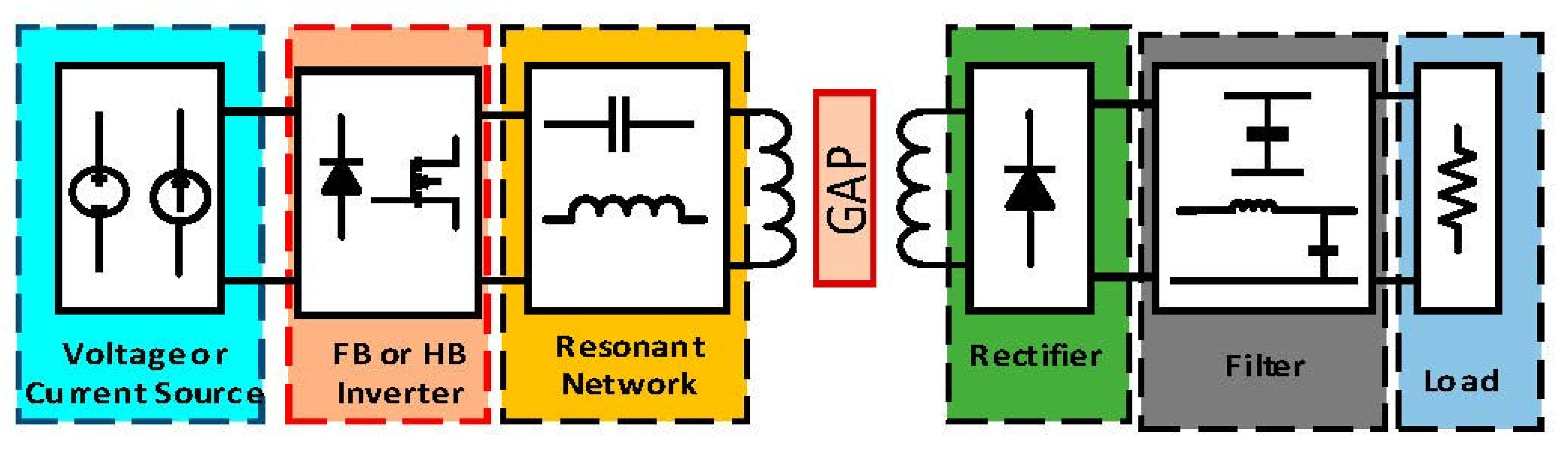
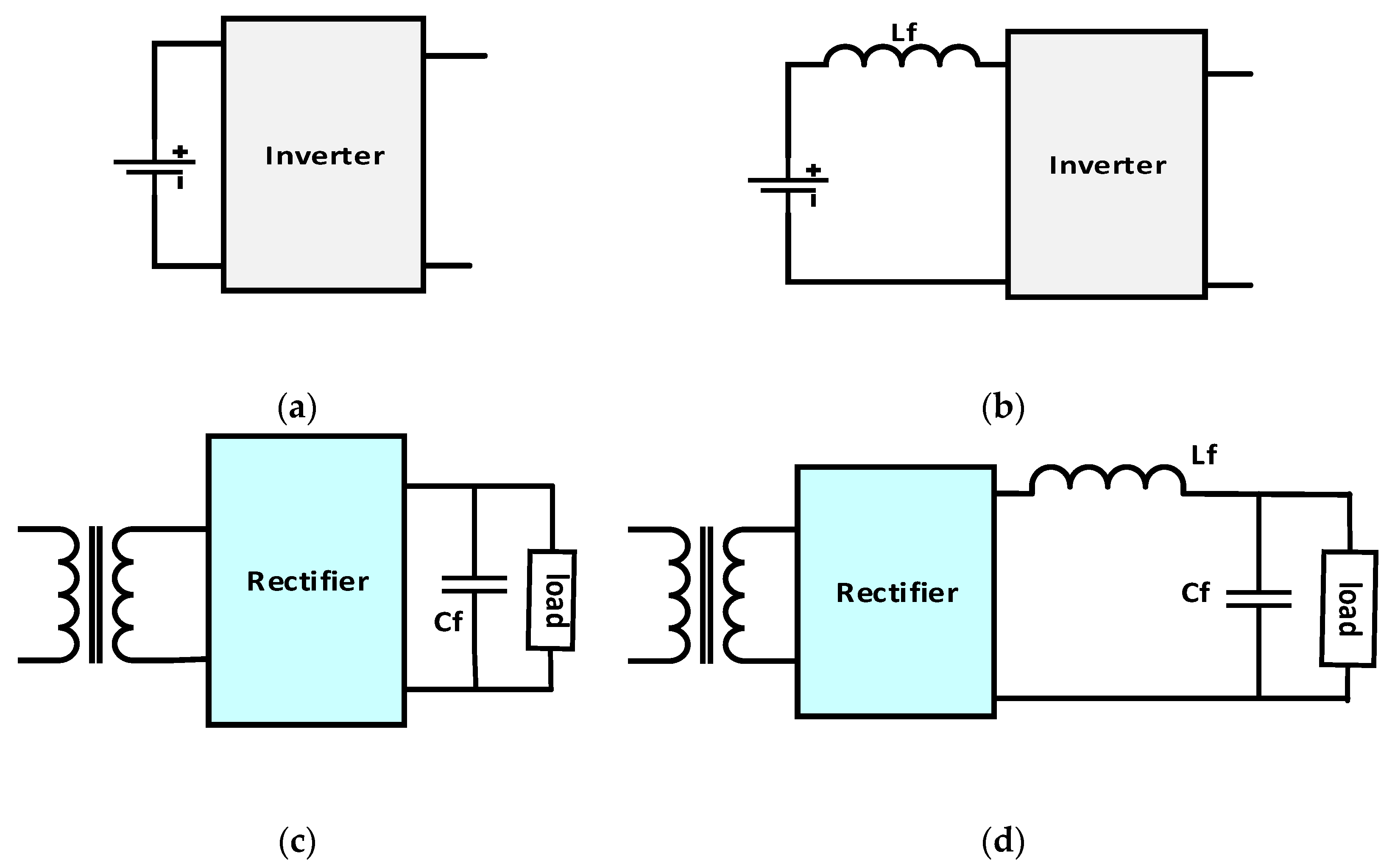
2. Theoretical Analysis of the IPRN

2.1. Analysis of an RN

According to [39], resonant and realizable are the necessary conditions for using an LC network as a resonant network (RN). To provide the above-mentioned requirements, the LC network is organized as follows: (1) prohibition of having cut set the inductor with a bi-level current resource/sink, and (2) prohibition of the inductor-paralleled with bi-level voltage resource, as well as the capacitor-series with bi-level current resource. However, the mentioned specifications do not imply the inefficiency of structures without the capability of meeting these criteria. It should be noted that they are not merely considered resonant networks. Therefore, identifying the type of sink and resource in the LC network terminals plays an important role in selecting the suitable topology. The resource/sink type-based diagram of RN block can be observed in Figure 2. According to the figure, the input can be the DC voltage or current resource, and the output can be voltage or current sink, which is applied through a rectifier and a filter.
The classification of RNs is in accordance with the types of resource and load; therefore, PRN classification can be as the following: (V-source/V-sink, V-source/C-sink, C-source/V-sink, and C-source/C-sink). The energy transmission within RPNs is conducted from the resource toward the load through the fundamental frequency, and the other part of harmonics can be neglected for all types of resources and sinks. Therefore, RN operation is considered as a low-pass or a band-pass filter that isolates both input and output at the harmonics of switching frequency.

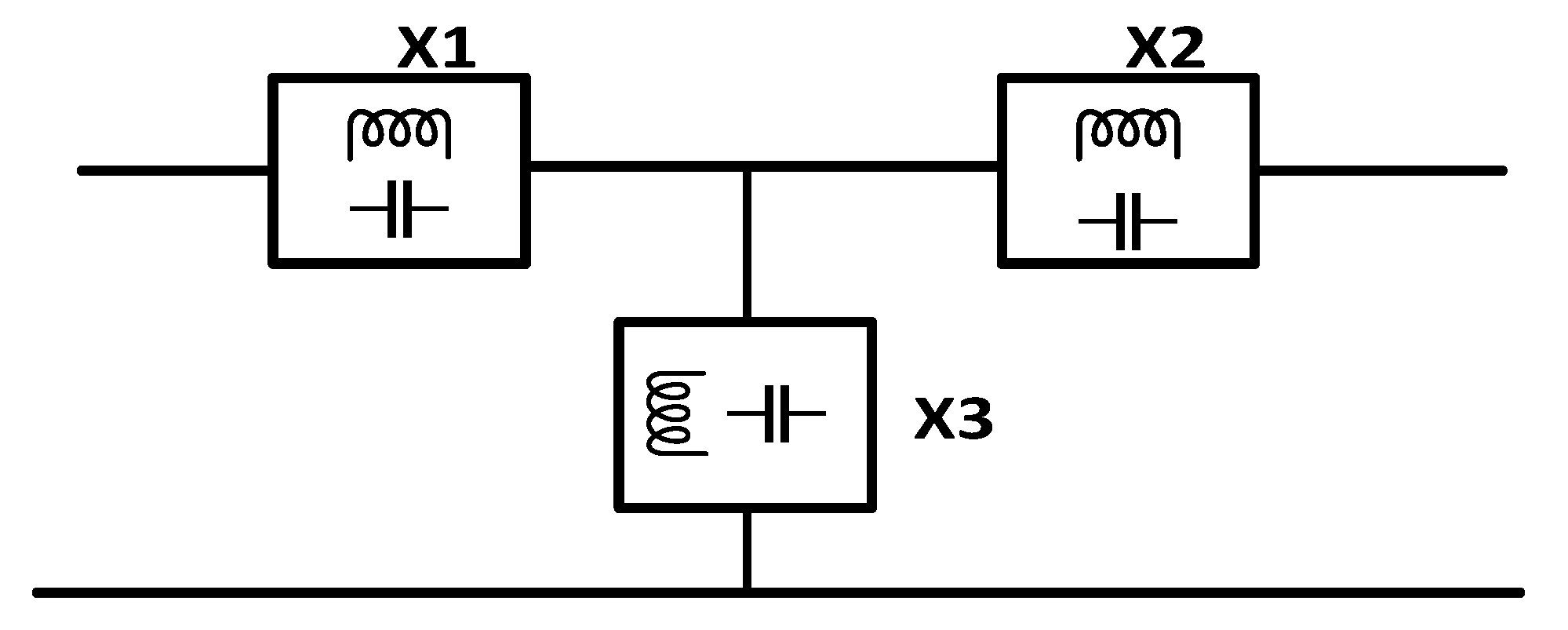
2.2. Analysis of an IPRN

A bipolar immittance network is illustrated in Figure 3 to index the two-port voltage and current expressions.
A network has an immittance property when voltages/currents are achieved as the following [40]:
( [ V 1 I 1 ] = [ 0 ± j Z 0 ± j Z 0 0 ] · [ V 2 I 2 ] ) ,   { V 1 = ± j Z 0 I 2 I 1 = ± j 1 Z 0 V 2
Considering Z0 as the base characteristic impedance of the network, it is realized that the output of the network depends merely on its input and is independent of its output impedance. This is very useful for power supply sources with a constant output voltage/current. It is well known that a quarter-wave distributed constant line exhibits immittance properties. While the length of the distributed constant line is manageable for operation in the megahertz range, it becomes prohibitively long for power converters operating in the kilohertz range. So, some lumped-element IRPN topologies based on the transmission line approximation competed using discrete inductors/capacitors have been discussed [41]. In addition, by expanding (1), the relationship between the input and output impedance in these networks is shown by the following relation:
Z 2 = V 2 I 2 = I 1 × Z 0 2 V 1 = Z 0 2 Z 1
Based on this equation, if the output impedance of the circuit is a resistive type, then the visited input impedance will be a resistive type. Therefore, according to Figure 1, the impedance observed from RN output is resistant against DC load, the output voltages/currents of the inverter are in phase, and the reactive power on the MOSFETs is minimized.
Transmission variables of PRN topologies should be derived first and then, RPN topologies with immittance can be achieved through substituting these variables within (1), which leads to achieving the consistent generation of current by a converter with the capability of load regulation.

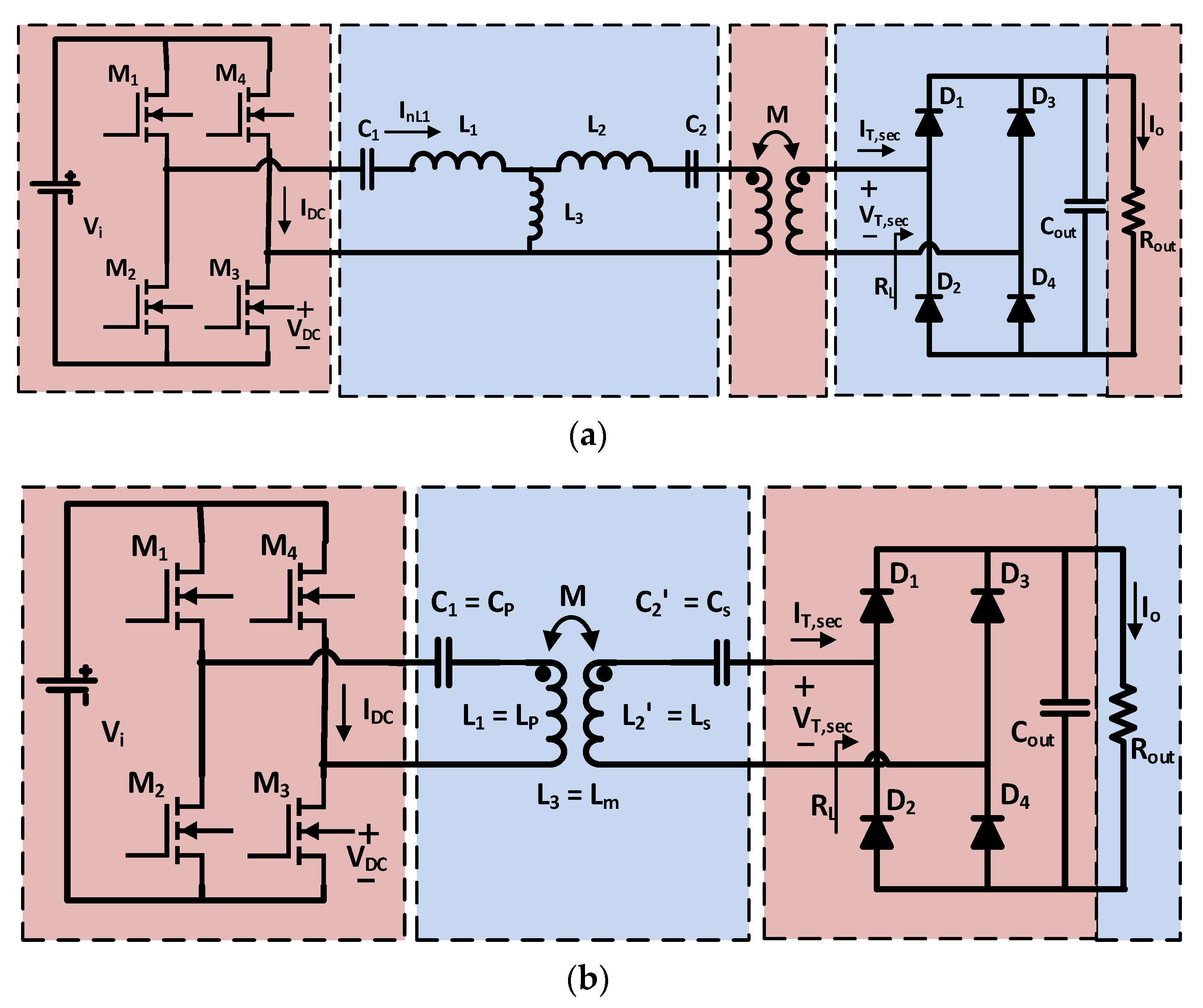
3. Design Conditions of IPRN Topologies in WPT System

An investigation of properties associated with different topological constructions is carried out in this section with the purpose of determining proper IPRN topologies within WPT applications. The basic condition for the presented search can be organized as follows:
PRN of type T is associated with a simple structure that contains fewer branches, low circulating currents, and increased capability of being integrated with parasitic elements; therefore, it is more beneficial. In Figure 4, the bipolar T-type PRN topology block diagram is shown. X1, X2, and X3 are the branch reactance impedances, which can be composited of capacitor/inductor.
Since an increased number of reactive components leads to the enhancement of converters’ size, weight, and costs, as well as the complexity of the analyzing and designing procedures, their maximum number is determined to be five. The immittance method can be implemented on all topologies with different resonance orders, but according to previous studies [40], low-order converters have shortcomings in terms of performance and control. Therefore, in Figure 5, fifth-order converters suitable for IPRN are provided.
The current study applied the immittance method in order to transform a voltage resource into a current one; therefore, the type of IPRN has to be voltage (V-source/C-sink) and (V-source/V-sink).
Figure 5 represents the fifth-order T-type topological structures required for WPTs, which are called T1–T12. However, the applicability of IPRN and non-IRPNs topologies is not mentioned although other types of IPRNs are widely applied.
In addition to the conditions mentioned, some characteristics for selecting topological superiorities for an appropriate application are organized as follows: (1) Ability to absorb parasitic elements, position the series inductor is connected to the right horizontal branch directly (T1, T4, T6, T8, T9, and T10), or indirectly, by transferring some of the reactive elements to the secondary side (T2, T5, and T12). This property is useful in the high current power supplies. (2) Ability to create an inherent DC blocking capacitor to prevent transformer saturation. Therefore, the cost and size are reduced by removing the external bulky capacitor. Thereby, topologies with connected series capacitors across the input port are preferred (T1, T4, T5, T7, T11, and T12). (3) A capacitor located on the left horizontal branch can also be used instead of bridge capacitors in the HB inverter circuit, which is the best choice for circuits based on current or voltage output applications (T1, T4, T5, T7, T11, and T12). (4) Ability to integrate the leakage and magnetizing inductances into the PRN elements, directly (T1, T2, T4, T5, T6, T10, and T12). This property is useful in the loosely coupled transformers, which decreases the number of reactive elements. It is evident from the above-mentioned findings that the topologies of T1–T12 can advantageously be proper for WPTs. Table 1 provides two circumstances required for the immittance-based continuous function of the current of T-type IPRNs with five branches. They are called the following: (1) Specific Operating Frequency (SOF), which is the appropriate switching frequency for the RN inverter, and (2) Suitable Reactive Elements (SRE), which represents a relation for selecting the appropriate reactive elements in each RN. To obtain these design conditions for each PRN topology, the base resonant frequency, i.e.,   ω r e is equal to 1 L 1 C 1 ,   and normalized switching frequency, i.e., ω n , s is equal to ω s w ω r e where ω s w is the switching frequency. The ratio of resonance tank elements i.e., α and β are given as follows:
α = L 2 / L 1
β = L 3 / L 1 ,   δ = L 4 / L 1 ,   γ = C 2 / C 1 , τ = C 3 / C 1
Table 1 shows that the topologies represented by Figure 4 with the immittance capability obeying mentioned conditions. Topologies (T5, T6, T9, and T10) have been eliminated due to the lack of the voltage-type (V-source/C-sink) and (V-source/V-sink) criteria.
By analyzing the phasor domain of each PRN and using the mentioned conditions, IPRN performance conditions are obtained. Each of these IPRNs, if used with these two conditions in the RN design, has an independent load current output. Finally, the best and most optimal structure for wireless power transmission is selected based on its design, modeling, analysis, and simulation provided further.

3.1. Analysis of the Proposed IPRN

The current study does not represent a comprehensive specification of eight IPRN topology design and analysis, although the same processes of IPRNs are demonstrated through a well-known compensation circuit (LCLCL-T) topology, T1, as the load-independent output current. T1 is the most similar topology to S/S compensation indirectly (transferring some of its reactive elements to the secondary part of the transformer). Considering the parasitic elements’ absorbance and preparation of inherent DC blocking to the transformer, the sample topology is selected and designed using the coupling coefficient, as well as the effects of the air gap and other core components. The proposed sample circuit diagram is shown in Figure 6. The full-bridge T1-IPRN circuit consists of two inductors of L1 and L2, which are in series with two capacitors C1 and C2, respectively. Moreover, L3 is a parallel inductor with a T-composite. The selected topology is the most adaptable structure in terms of complete modeling of transformers instead of L1, L2, and L3. The leakage inductances of transformer are applied as elements of RN (L1, L2) and primary-side magnetizing inductance (Lm) as L3. Therefore, leakage inductors and parasitic elements are reduced, resulting in minimal losses and higher output efficiency.

3.2. Achieving Mathematical Equations

Simple and precise analysis methods such as Fundamental Mode Approximation (FMA), and structures with the minimum number of branches and low circulating current, such as T-type, have been used to achieve the equations of current and voltage output and governing relationships between the proposed circuit elements. To start the design process via this method, Transmission parameters of the proposed topology are investigated. Transmission parameters (ABCD parameters) of a bipolar network are defined as:
[ V 1 I 1 ] = [ A C B D ] . [ V 2 I 2 ]
where parameters (A, B, C, and D) are reverse voltage gain, transfer impedance, transfer admittance, and reverse current gain, respectively. Compared with (1), in order to have immittance properties, the transmission parameters can be written as:
A = D = 0, B × C = 1.
Therefore, based on (4), the transmission parameters of T1 as a sample of T-type in Figure 4 are derived as:
A = ( 1 + X 1 X 3   ) ,   B = ( X 1 X 2 + X 1 X 3 + X 2 X 3 X 3 ) ,   C = ( 1 X 3 ) ,   D = ( 1 + X 2 X 3 )
Next, by applying condition (5), it is concluded that T1 can exhibit immittance conversion characteristics if,
X1 = X2 = −X3
Therefore, T1 exhibit immittance properties only if its reactance satisfy the respective condition given in (7) and Table 1. For simplifying the analysis with the purpose of deriving the following relationships in the normalized form, the base voltage and current are used as Vi and (   V i Z 0   ) , respectively. Additionally, ( Z 0 = L 1 C 1 ) is defined as the following [40], the quality factor (Q) and equivalent AC resistance seen from the primary side of transformer (RL) can be expressed as:
Q = n 2 Z 0 R o u t ,   R L = 8 R o u t n 2 π 2  
Then, the RMS value of input voltage, output current, and the normalized output current is given as follows:
V i , r m s = 2 2   V i π ,   I o = 2 2 π I R L n , I o n = n I o V i Z 0
By writing the resonance network equations as well as altering the defined parameters (3), the normalized output current is illustrated as follows:
I o n = 8 j γ β ω n 3 π 2 [ 1 ( 1 + α γ + β + β γ ) ω n 2 + ( α γ + β γ + α β γ ) ω n 4 + j 8 γ π 2 Q   ( ω n ( 1 + β ) ω n 3 ]  
According to (10), the output current is irrelevant to the load under the conditions of Table 1, by replacing the SOF and SRE. Therefore, the normalized output current under immittance conditions is given as follows:
I o n / ω n = 1 1 + β   ,       α = 1 + β β γ γ   = 8 ( 1 + β ) j π 2 β
In this state, the output current only depends only upon ( β ). Therefore, achieving the output current can be controlled by adjusting ( β ). Moreover, higher design flexibility is one of the achievements of this feature. The current observed within L1, and C1 is summarized as the following through regulated RMS voltage/current as follows:
I n L 1 = I L 1 , r m s V i Z 0 = 2 2 π [   8 γ ω n 2 π 2 Q   ] + j [ ω n γ ( β + α ) ω n 3 ] A 1 + j A 2
where
A 1 = 1 ( 1 + α γ + β + β γ ) ω n 2 + ( α γ + β γ + α β γ ) ω n 4  
A 2   = 8 γ π 2 Q   ( ω n ( 1 + β ) ω n 3 )
Next, the phase angle between T1 input current and voltage, which is in SOF, can be derived as follows:
θ = A r c t g ( π 2 Q ( 1 + β ) γ ( β + α ) 8 γ ( 1 + β ) ( 1 + β ) )
Equation (15) reveals that ( θ ) is zero under the SRE condition. In other words, the conduction losses are in the least possible values.
One of the optimal design methods is to minimize the circuit size through the quantity reduction of reactive components. Elements with the ratios of apparent and active power (KVA/KW) are defined as the maximum power transmission basis (MPTB) index, which can be achieved as the following index:
M P T B = K V A K W = x = 1 3 ( V n L x × I n L x ) + x = 1 2 ( V n C x × I n C x ) I o n 2 Q  
The normalized current and voltage relations of IPRN components in conventional and immittance circumstances with the replacement of SOF and SRE can be observed in Table 2. According to this table, MPTB is obtained as:
M P T B = 16 ( 1 + β ) 1 + β π 2   Q   β 2 + π 2   2 Q   ( β + α ) 8   1 + β  
As can be seen from (17), the MPTB value is the function of ( α , β , and Q). Given the dependence of Q on the load, it is found that Q is the only variable parameter throughout the circuit operation that changes the value of MPTB; therefore, the optimal Q function can be obtained as follows:
Q o p t i m u m = 8 ( 1 + β ) π 2 β β + α  
Using the optimum Q value, MPTB and the physical size of the circuit elements are minimized which can lead to the maximum power transfer, which is the objective of the proposed system. Accordingly, the following relationships can be obtained as the following:
t r a n s f o r m e r   t u r n   r a t i o :   n = I o × R o m a x V i 1 + β β + α  
L 1 = 4 π 3 β + α 1 + β V i 2 I o 2 R o m a x f s β  
C 1 = π I o 2 R o m a x β 16   V i 2 f s ( β + α ) ( 1 + β )  
where Romax is the maximum load resistance and fs is the switching frequency.

3.3. Parameter-Tuning Process

Using the relationships obtained in the previous section, the values of L2, L3, and C2 can be calculated. These parameters are a function of ( α , β , and γ ) . Furthermore, all transformer parameters are expressed as functions of K [42]. Therefore, the relations governing a transformer with a similar magnetic structure within the two initial and secondary parts can be achieved as the following
L p / L s N p 2 / N s 2 = 1 n 2 , M = K L p × L s  
where Lp, Ls, and M are the leakage-inductance primary side, leakage-inductance secondary side, and mutual inductance of the transformer, respectively. The Primary-side magnetizing inductance, i.e., Lm and M can be estimated as follows:
Lm K × L p ,   M n K L p  
where K is the actual coupling coefficient.
Assuming K0 as the proper coupling coefficient at the designed operating point with the purpose of achieving suitable α , β , and γ values with respect to K0, the significant points are:
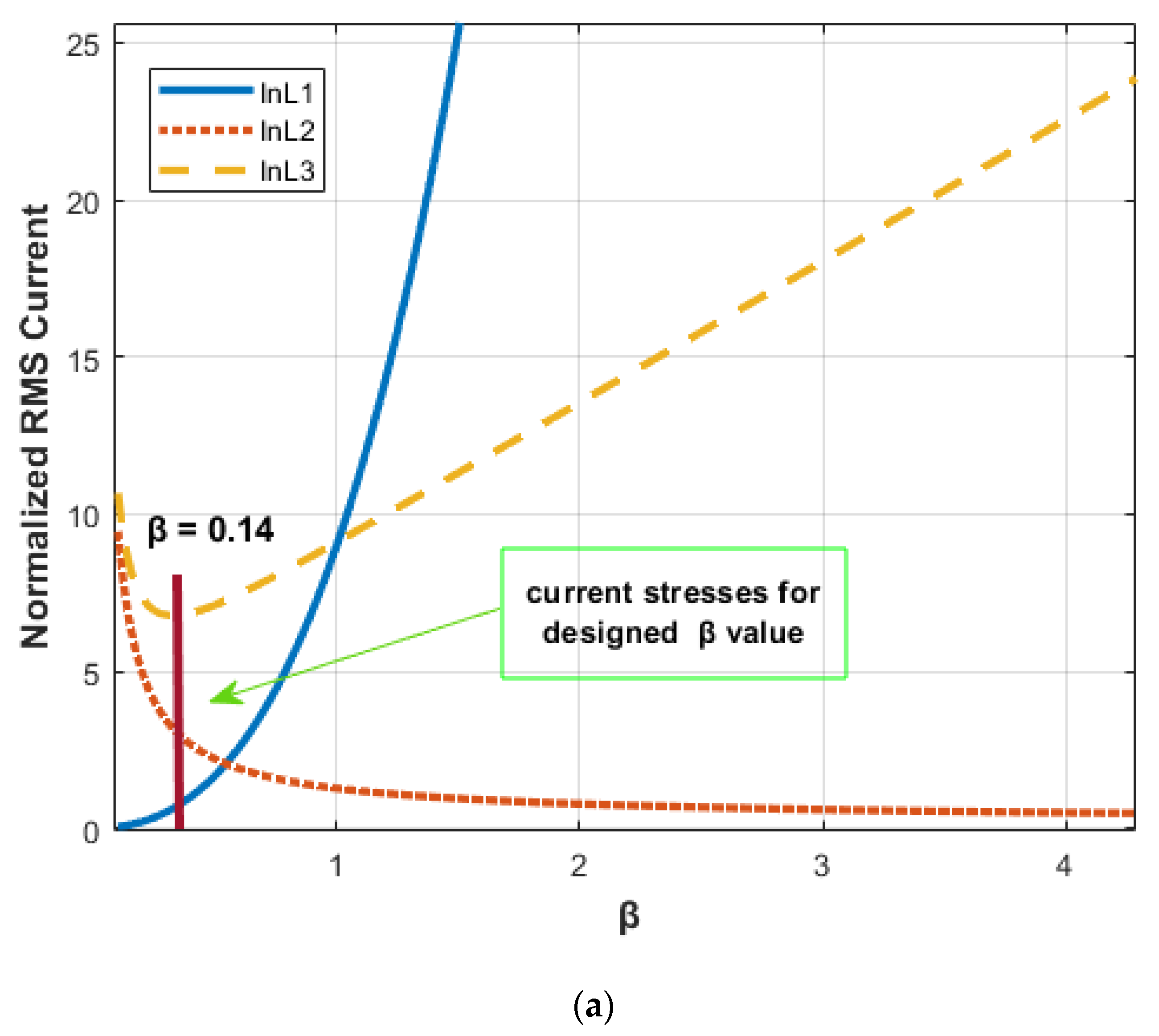
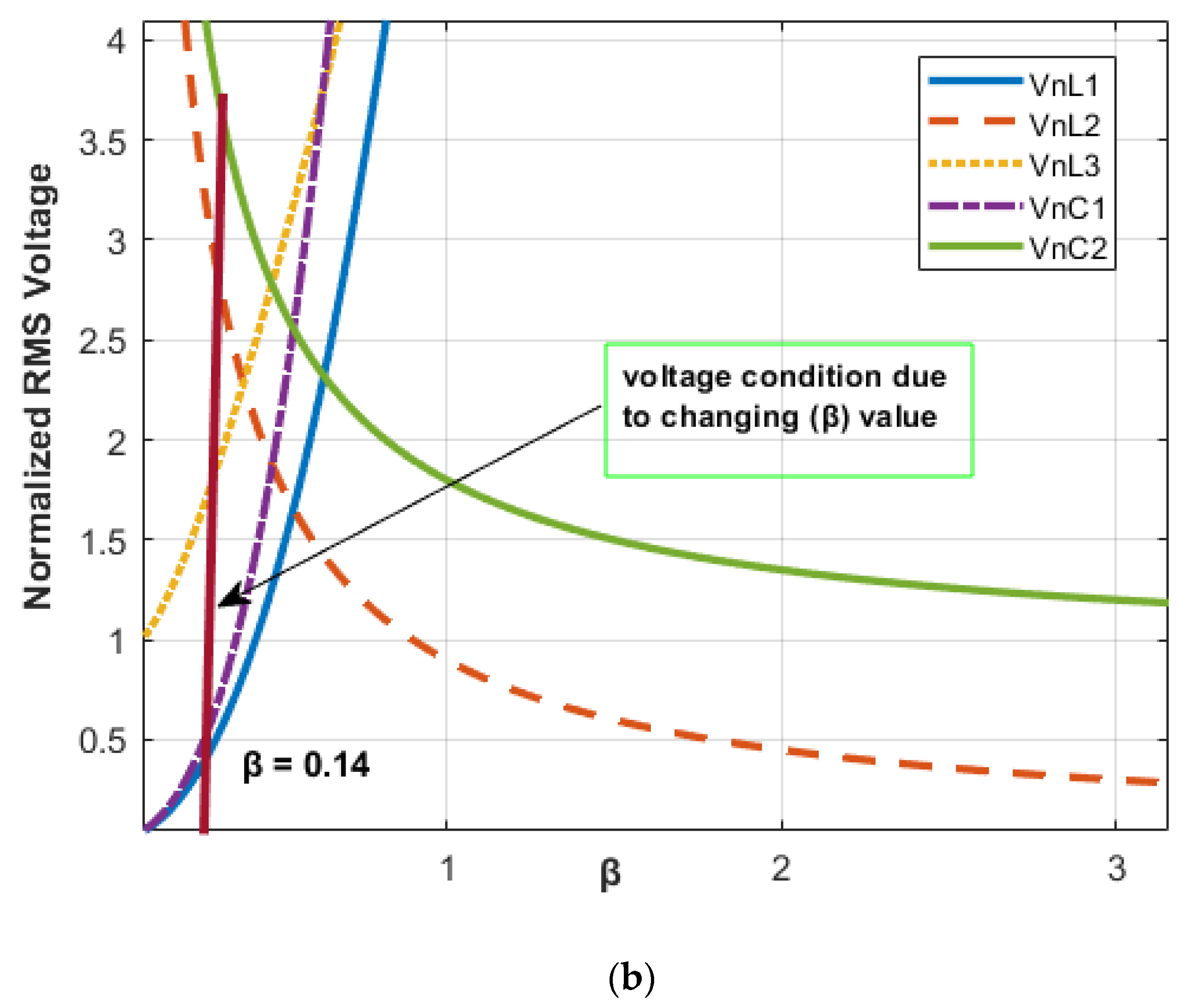
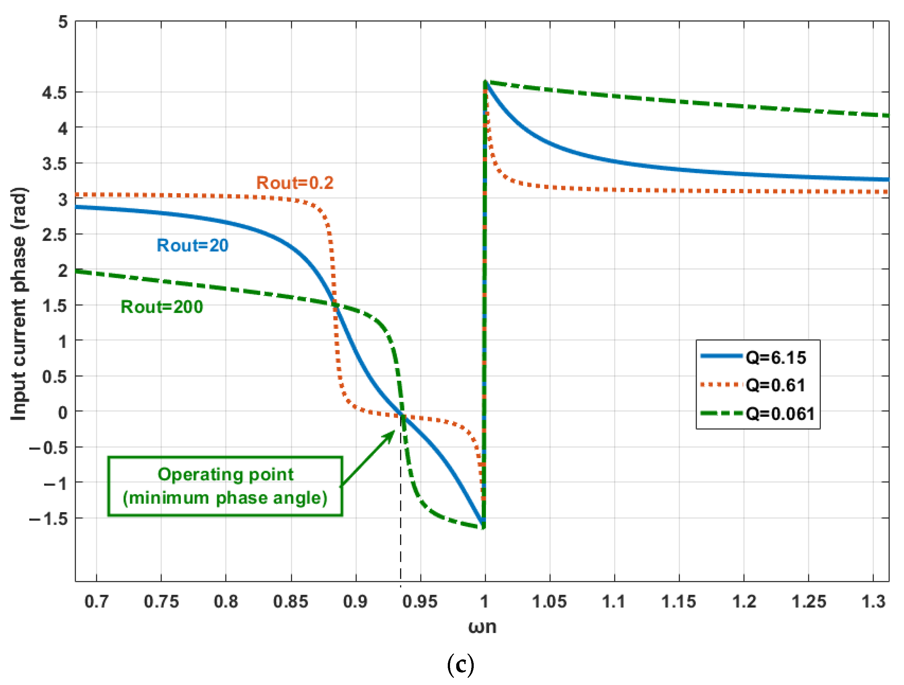
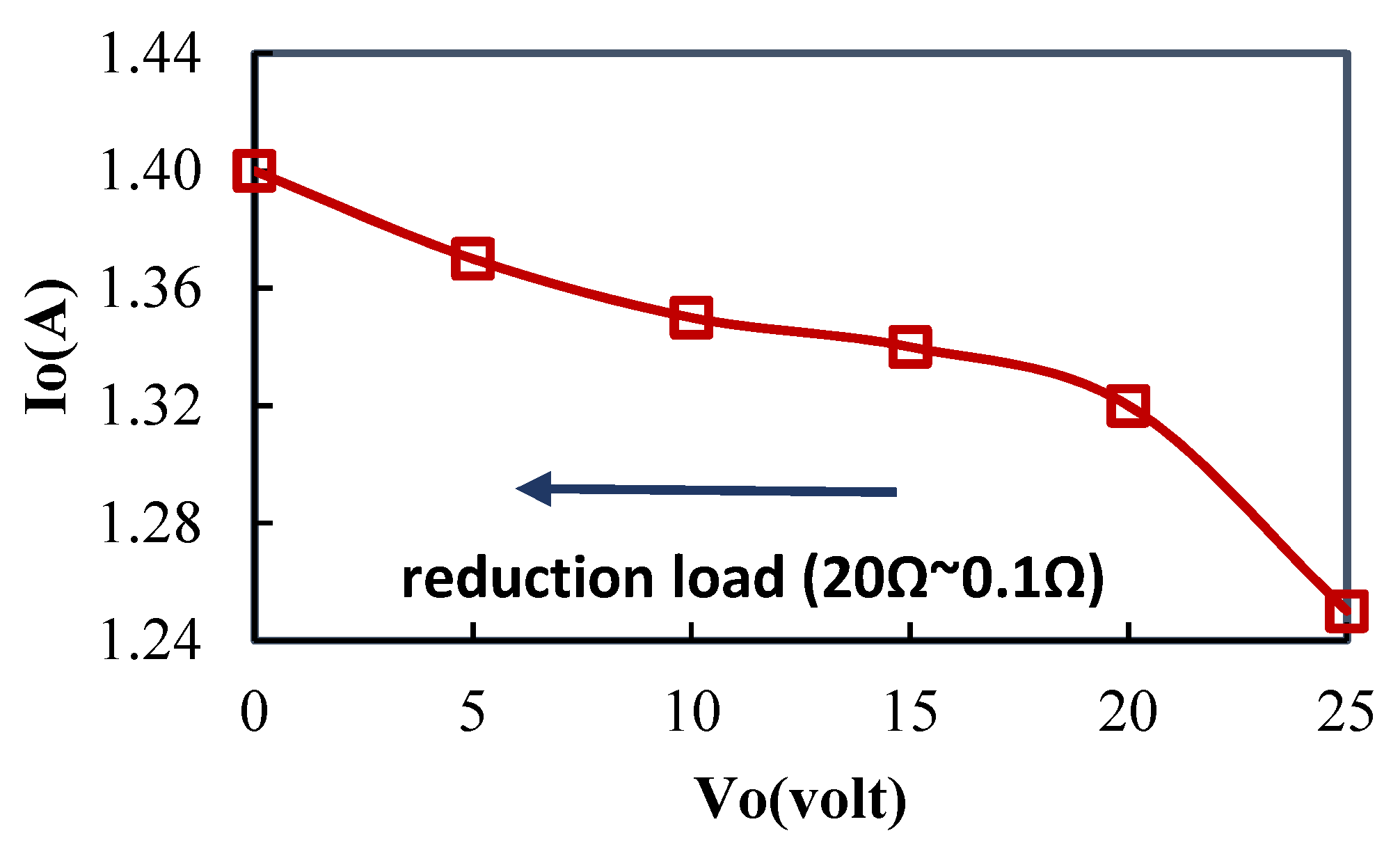
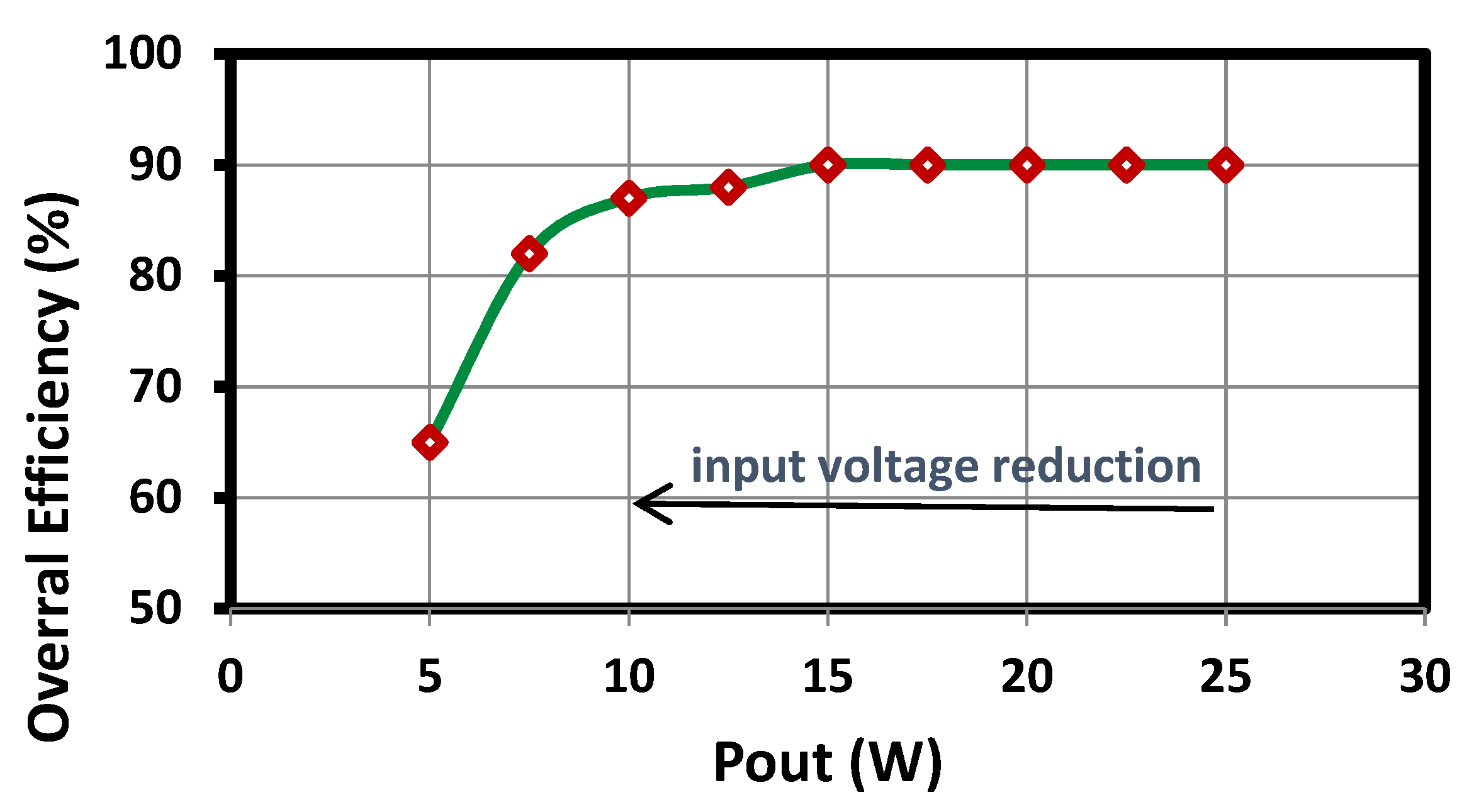
  • The minimum voltage and current stresses can be realized with well-designed parameters. Table 2 shows that selecting the proper β can considerably decrease the voltage/current stresses on the components. The stresses of voltage/current parameters are directly related to ( β ). Due to the relationship between L1 and L2 with Lp and Ls (based on Section 3.1), therefore, the possible value range of β should be selected according to the rated Lp and Ls and subsequently, is related to the volumes and dimensions of primary and secondary coils. According to practical limitations, the values obtained at the 30 mm air gap for the proposed ferrite core in the laboratory, the value of 0.14 is appropriate for ( β ). It is noteworthy that regulated voltage/current stresses on T1 components under different ( β ) values, which are within immittance mode under the steady-state output circumstances, were presented and compared in Figure 7. These diagrams are extracted from Table 3. A significant observation from Figure 7 is that the current and voltage stresses decrease with the   β reduction.
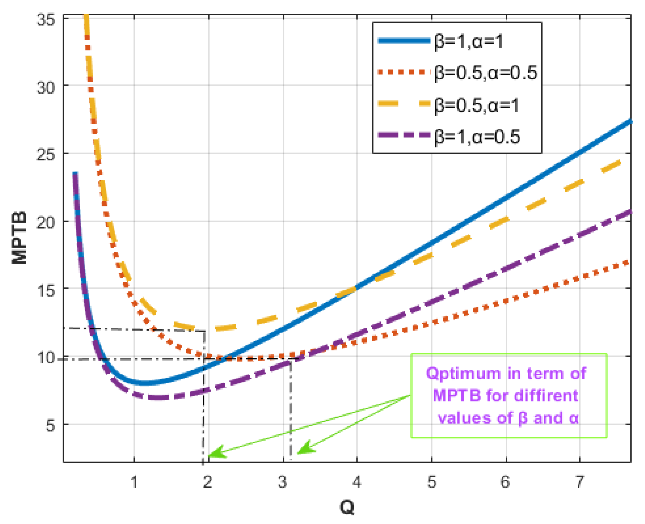
  • K0 selection must be carried out to decrease the stresses resulting from voltage/current. Therefore, the regulated voltage/current values of components with respect to K0 and Qoptimum are summarized in Table 3. According to (17), the Qoptimum is the function of α and β . Using Figure 8, proper values for α and β can be achieved. Figure 8 indicates the relationship between MPTB and Q of various quantities of β and α . It can be inferred that higher and lower values of β and α must be considered, respectively, while performing the designing procedure. Also, to achieve a reduction in the physical size of the circuit, it is necessary to select the lower Qoptimum value. Since β is proportional to K0, the regulation procedure must be conducted with the purpose of achieving the appropriate coupling coefficient.
Figure 7. Normalized voltage and current stresses on the proposed IPRN elements versus β . (a) Currents; (b) voltages.
Sustainability 14 09391 g007aSustainability 14 09391 g007b
Figure 8. Quality factor diagram in terms of the physical size of elements for different values of β and α .
Sustainability 14 09391 g008
To find the values of suitable and optimal elements, T1 circuit is simulated. The proposed circuit is associated with a number of definitions including the input DC supply voltage (Vi) = 20 V, Io = 1.4 A, Ro,max (full load) = 20 Ω, fs = 100 kHz. Ten simulations have been performed for the different α , β , and γ values to achieve proper perspective in the selection of parameters. With the help of simulation results, it can be found that the optimal values for α , β , and γ are determined to be 1, 0.14, and 1, respectively. It should be noted that in practice, the input current is required to slightly lag the input voltage and consequently, achieve ZVS. The required phase lag is achieved through a slight reduction of γ .
Figure 9 represents the regulated output current (Ion), as well as the phase angle between IPRN input current and voltage (θ); also, it indicates that there is an independent output current, and the input voltage is nearly in phase with the input current. In other words, the phase angle of the input current and voltage is zero under immittance conditions (SOF and SRE) in various loads. Therefore, the proposed resonant compensation tank has eliminated most of the reactive power.
It can be found from Figure 9 that the output current is constant at around 100 kHz and the proposed WPT system can maintain the immittance mode in a proper range ( ± 4   kHz )   of frequency. Therefore, low-frequency changes do not affect the circuit performance. Moreover, according to Figure 9b, the voltage plot indicates the behavior of CV mode in the frequency range of 82 kHz and 93 kHz. Also, CC and CV characteristics can be derived. Therefore, the proposed research is employed in order to transform a voltage resource to a current resource, or conversely.

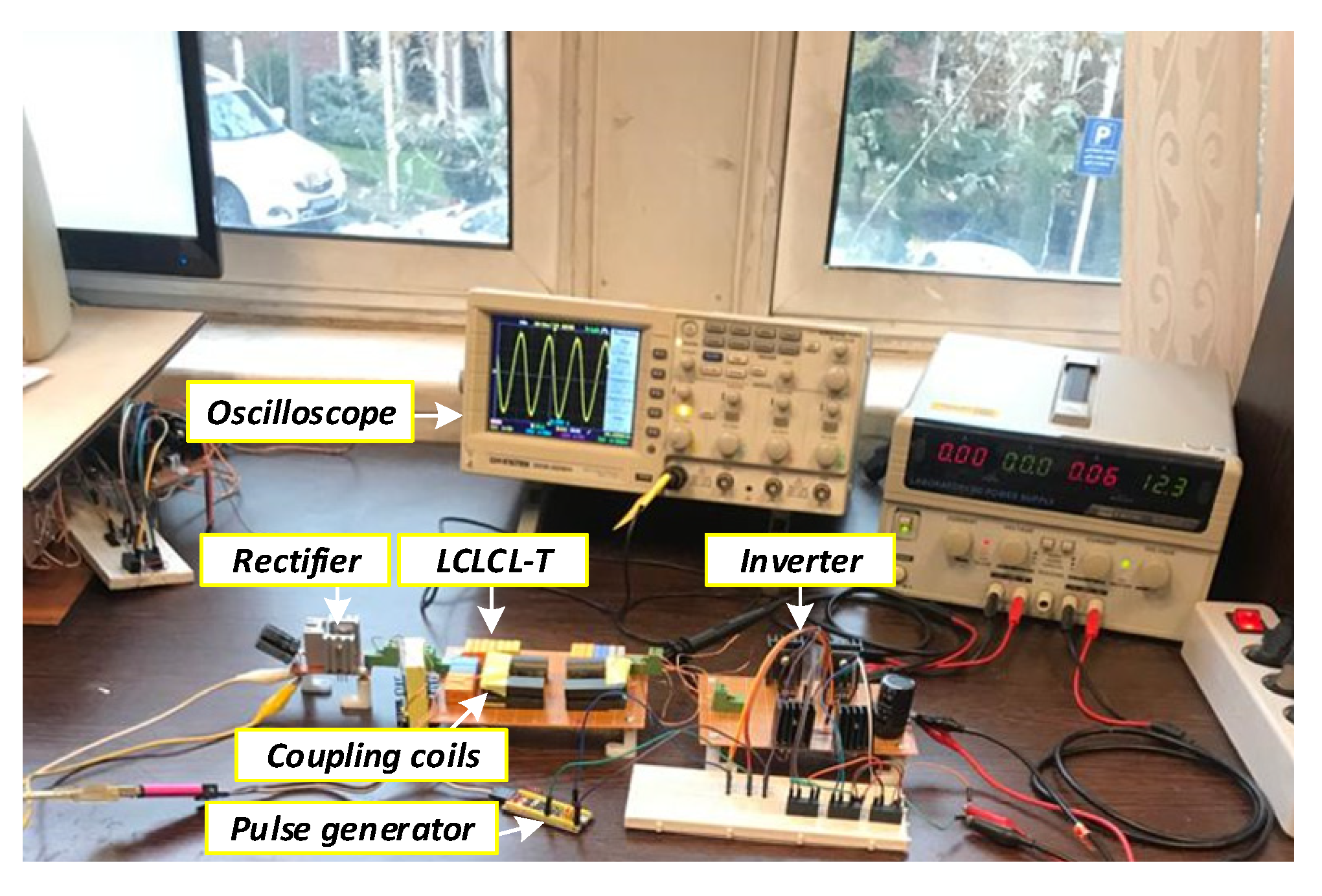
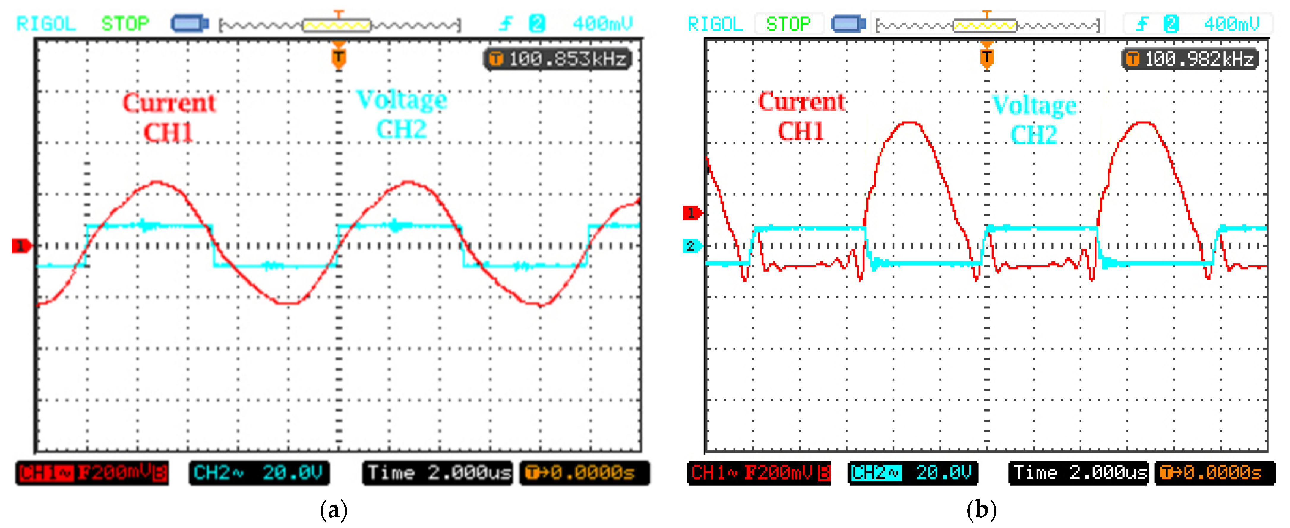
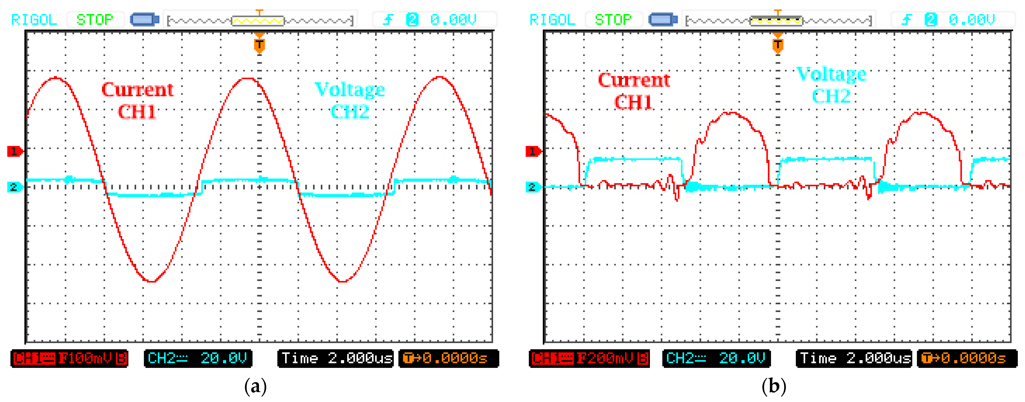
4. Experimental Verification

4.1. Practical Result

Designed values of the proposed circuit elements in Table 3 are implemented on the sample circuit. IPRN topology operates at an input voltage of 20 V DC using a full-bridge inverter. The output power of 25 W at 20–50 mm in a U-shaped transformer is transmitted to load 30 Ω with different coupling coefficients using a 38AWG Litz-wire. We are aware that large samples in range of about 5 kW are also made for WPT systems, but due to the limitations of the laboratory and equipment, a small sample is considered as a test. The IPRN practical example is shown in Figure 10. Considering L1, L2, and L3 as the values of primary and secondary and magnetizing inductances of the transformer, the number of elements used in the construction is reduced. By using an RLC meter, the inductance and internal resistance of the coils are measured as follows: LP = 103 µH, LS = 183 µH, RLp (Primary coil DC ESR) = 27.8 mΩ, and RLs (Primary coil DC ESR) = 53.2 mΩ. The coupling coefficient is also practically adjusted using the air gap. With the 30 mm air gap and the windings 23 and 35 that turn onto the initial and secondary cores, desired values of the proposed circuit are achieved. The M1 ~ M4 MOSFETs with a frequency of about 100 kHz are switched on by the HCPL-3120 and Micro ATmega32A drivers and a square wave with the amplitude of Vi is supplied to the RN input. The values and types of elements applied to the proposed IWPT can be observed in Table 4.
IPRN practical graphs in the minimum coupling coefficient at maximum load are indicated in Figure 11. The ZVS realization for switches and the maximum coherence of the transformer output voltage and current result in minimal loss of rectifier diodes. In the output resistance mode, the output current is about 1.33 A and the efficiency is 90%. Figure 12 shows the practical outputs with a maximum load of 5% condition. The range of the current load is 1.4 A, while the efficiency is 64%. The input current that is in phase with the voltage across the power MOSFET M3 is also observed after the decrease of load and input current, which suggests the ability to adjust the load and independent load. Similarly, the output current seems to be almost unchanged at different loads; thus, it proves the characteristics of the current resource. However, the current load is mathematically fixed regardless of the load change; therefore, it experimentally falls with output due to the IPRN component losses.
The feedback-free output parameters of the practical sample achieved at different loads can be observed in Figure 13. It was expected that IPRNs constant current with a reduced load leads to the decrease of the input current, which indicates that the output current is only a function of the input voltage. This demonstrates the superiority of this topology with its current output tuning using a cheap commercial ferrite core. The minor changes in the output current are due to the non-ideal elements and loss of circuit connections.
The output power, Pout, and efficiency, η, are calculated versus load variations by using:
η = P o u t P i n = I o 2 × R o u t V i × I i
The overall efficiency of the prototype is measured via a power meter versus the output power transfer, in the full-load condition is illustrated in Figure 14. This plot indicates the T1 high efficiency in various operating powers. The relative efficiency drop, especially in low input voltages, is due to the comparable voltage drops with the reduced output voltage.
Since there is a high circulating current within the initial part of the converter, the efficiency decreases with the reduction of the coupling coefficient. This diagram shows the IPRN optimal efficiency for different performance powers. Moreover, the current decreases with the load power, and it leads to the maintenance of increased converter effectiveness over the extensive fluctuations of generated power. It is noteworthy that the prototype’s maximum load effectiveness is determined to be 0.9. Details of system losses have been measured via a power meter in the laboratory and are illustrated in Figure 15. There was a total of 2.75 w of power dissipated in this 25 w sample, accounting for 0.75 w of inverter losses, where the conduction loss in D1 through D4 was estimated to be 0.75 w. Finally, most of it was wasted by around 1 w in the core and winding. Therefore, this figure shows the full-bridge inverter losses, magnetic coupler losses, and rectifier losses account for a large proportion of the total system losses. These results are also similar to the literature [42]. Therefore, the proper design of the transformer, inverter, and rectifier should be considered to improve the efficiency of the system.

4.2. Discussion and Comparison

To evaluate and verify the effectiveness of the proposed technique over the conventional approach to designing a load-independent output current topology for wireless power transfer (WPT) systems, T1-RN in immittance mode and an S/S topology in the conventional approach presented in [43] are compared. Under the same comparative conditions, the following can be deduced: (1) one of the main deficits of S/S resonant compensation is decreased load regulation despite controlling the frequency [40]. However, the protection from short-circuit is achieved through T1. Also, it is associated with inherent constant current characteristics under immittance circumstances, which leads to the elimination of deficits of the major S/S compensation in the process of light-load regulation. The results obtained at 1% of the full load are evidence to prove this case. (2) According to [43], maximum efficiency can exist at w = wm, which is obtained by deriving efficiency from operating frequency. The expresses have indicated that wm is dependent on the load. Therefore, in a conventional mode for achieving maximum efficiency, it is assumed that proper frequency tracking is performed by complex control methods. However, in the method discussed in this paper, obtaining the Qoptimum, reducing the physical dimensions of the circuit, and increasing the efficiency have been achieved. (3) According to [43], the current gain of the S/S compensation is inversely proportional to K, therefore when K varies, the output current also varies. However, due to the current gain, and Table 3, can be observed:
G ( i m m i t t a n c e   m o d e ) = 8 π 2   1 + β β      
                                      G K = 4 π 2   ( K + 1 ) ( 1 + K ) 1 2       ,     S K G = 1 2        
where S K G is the current gain sensitivity to K.
Therefore, the output current is independent of the coupling coefficient at the designed operating point. The comparative points mentioned above show that the IPRN topologies are superior in terms of load regulation, efficiency improvement based on the optimal quality factor, and effective coupling range.

5. Conclusions

A mathematical method based on immittance property to obtain an independent output current for wireless power transfer (WPT) systems is investigated in the current study. Compared to complex regulation methods, the IPRN technique is associated with uncomplicated designation; also, it is more cost-effective and is carried out based on component size minimization. The realizable and resonant T-type PRNs were identified first. Then, the process of analyzing related circumstances of immittance operation is carried out by considering the transformer coupling coefficient at different air gaps. Due to the capability of integrating the resonant inductors into the single magnetic component, as well as an inherent DCB for the isolation transformers, a structure was selected. Using the MPTB index, which was based on reducing the physical dimensions of the converter, LCLCL-T topology with appropriate reactive element values was designed and applied to a WPT system including a full-bridge inverter, capacitor-based compensation circuits, series-series capacitor-based compensation circuits, and DC load. It was confirmed through conducted experiments and the steady-state simulation that there was a current-resource behavior associated with the system, as well as ZVS of all active switches under variations of the loading. Finally, the properties of the proposed scheme could be summarized as follows: (1) ability to absorb parasitic components; (2) the minimized device switching loss and stresses; (3) adapted for use as a constant current power source; (4) the inverter output current and voltage were almost in phase, which indicated the achievement of the loads’ active power through the inverter. Moreover, compared to conventional topologies, the IPRN topologies are superior in terms of load regulation, efficiency improvement by optimizing the parameter tuning.

Author Contributions

Methodology, Supervision and Funding acquisition, S.M.H.H. and J.O.; Writing—review and editing L.Y. Data Collection, B.M. All authors have read and agreed to the published version of the manuscript.

Funding

This research received no external funding.

Institutional Review Board Statement

Not applicable.

Informed Consent Statement

Not applicable.

Data Availability Statement

The data presented in this study are available on request from the Corresponding author. The data are not publicly available due to privacy restrictions.

Conflicts of Interest

The authors declare no conflict of interest.

References

  1. Liu, H.; Huang, X.; Tan, L.; Guo, J.; Wang, W.; Yan, C.; Xu, C. Dynamic Wireless Charging for Inspection Robots Based on Decentralized Energy Pickup Structure. IEEE Trans. Ind. Inform. 2018, 14, 1786–1797. [Google Scholar] [CrossRef]
  2. Zhang, Y.; Tian, G.; Lu, J.; Zhang, M.; Zhang, S. Efficient Dynamic Object Search in Home Environment by Mobile Robot: A Priori Knowledge-Based Approach. IEEE Trans. Veh. Technol. 2019, 68, 9466–9477. [Google Scholar] [CrossRef]
  3. Huang, S.; Lee, T.; Li, W.; Chen, R. Modular On-Road AGV Wireless Charging Systems Via Interoperable Power Adjustment. IEEE Trans. Ind. Electron. 2019, 66, 5918–5928. [Google Scholar] [CrossRef]
  4. Siroos, A.; Sedighizadeh, M.; Afjei, E.; Fini, A.S. Comparison of different controllers for wireless charging system in AUVs. In Proceedings of the 2022 13th Power Electronics, Drive Systems, and Technologies Conference (PEDSTC), Tehran, Iran, 1–3 February 2022; pp. 155–160. [Google Scholar]
  5. Tang, Y.; Chen, Y.; Madawala, U.K.; Thrimawithana, D.J.; Ma, H. A New Controller for Bidirectional Wireless Power Transfer Systems. IEEE Trans. Power Electron. 2018, 33, 9076–9087. [Google Scholar] [CrossRef]
  6. Esmaeil, J.; Salehizadeh, M.R.; Rahimikian, A. Optimal control of the power ramp rate with flicker mitigation for directly grid connected wind turbines. Simulation 2020, 96, 141–150. [Google Scholar]
  7. Chen, X.; Huang, D.; Li, Q.; Lee, F.C. Multichannel LED driver with CLL resonant converter. IEEE J. Emerg. Sel. Top. Power Electron. 2015, 3, 589–598. [Google Scholar] [CrossRef]
  8. Haga, H.; Kurokaw, F. Modulation method of a full-bridge three-level LLC resonant converter for battery charger of electrical vehicles. IEEE Trans. Power Electron. 2017, 32, 2498–2505. [Google Scholar] [CrossRef]
  9. Hou, J.; Chen, Q.; Zhang, Z.; Wong, S.; Tse, C.K. Analysis of Output Current Characteristics for Higher-Order Primary Compensation in Inductive Power Transfer Systems. IEEE Trans. Power Electron. 2018, 33, 6807–6821. [Google Scholar] [CrossRef]
  10. Li, Y.L.; Sun, Y.; Dai, X. μ-Synthesis for Frequency Uncertainty of the ICPT System. IEEE Trans. Ind. Electron. 2013, 60, 291–300. [Google Scholar] [CrossRef]
  11. Huang, Z.; Lam, C.; Mak, P.; Martins, R.P.d.S.; Wong, S.; Tse, C.K. A Single-Stage Inductive-Power-Transfer Converter for Constant-Power and Maximum-Efficiency Battery Charging. IEEE Trans. Power Electron. 2020, 35, 8973–8984. [Google Scholar] [CrossRef]
  12. Lourdusami, S.S.; Viaramani, R. Analysis, design and experimentation of series-parallel LCC resonant converter for constant current source. IEICE Electron. Exp. 2014, 11, 20140711. [Google Scholar] [CrossRef] [Green Version]
  13. Duan, F.; Xu, M.; Yang, X.; Yao, Y. Canonical model and design methodology for LLC DC/DC converter with constant current operation capability under shorted load. IEEE Trans. Power Electron. 2016, 31, 6870–6883. [Google Scholar] [CrossRef]
  14. Li, Y.; Xu, Q.; Lin, T.; Hu, J.; He, Z.; Mai, R. Analysis and Design of Load-Independent Output Current or Output Voltage of a Three-Coil Wireless Power Transfer System. IEEE Trans. Transp. Electrif. 2018, 4, 364–375. [Google Scholar] [CrossRef]
  15. Salehizadeh, M.R.; Koohbijari, M.A.; Nouri, H.; Taşcıkaraoğlu, A.; Erdinç, O.; Catalao, J.P. Bi-objective optimization model for optimal placement of thyristor-controlled series compensator devices. Energies 2019, 12, 2601. [Google Scholar] [CrossRef] [Green Version]
  16. Naghash, R.; Alavi, S.M.M.; Afjei, S.E. Robust Control of Wireless Power Transfer Despite Load and Data Communications Uncertainties. IEEE J. Emerg. Sel. Top. Power Electron. 2021, 9, 4897–4905. [Google Scholar] [CrossRef]
  17. Jamakani, B.E.; Afjei, E.; Mosallanejad, A. A Novel Triple Quadrature Pad for Inductive Power Transfer Systems for Electric Vehicle Charging. In Proceedings of the 2019 10th International Power Electronics, Drive Systems and Technologies Conference (PEDSTC), Shiraz, Iran, 12–14 February 2019; pp. 618–623. [Google Scholar]
  18. Zhang, W.; Mi, C.C. Compensation topologies of high-power wireless power transfer systems. IEEE Trans. Vehicular Tech. 2016, 65, 4768–4778. [Google Scholar] [CrossRef]
  19. Mahdizadeh, A.H.; Afjei, E. LLC Resonant Converter Utilizing Parallel-Series Transformers Connection. In Proceedings of the 2019 International Power System Conference (PSC), Tehran, Iran, 9–11 December 2019; pp. 472–477. [Google Scholar]
  20. Ramezani, A.; Farhangi, S.; Iman-Eini, H.; Farhangi, B.; Rahimi, R.; Moradi, G.R. Optimized LCC-Series Compensated Resonant Network for Stationary Wireless EV Chargers. IEEE Trans. Ind. Electron. 2019, 66, 2756–2765. [Google Scholar] [CrossRef]
  21. Nagatsuka, Y.; Ehara, N.; Kaneko, Y.; Abe, S.; Yasuda, T. Compact contactless power transfer system for electric vehicles. In Proceedings of the The 2010 International Power Electronics Conference-ECCE ASIA-, Sapporo, Japan, 21–24 June 2010; pp. 807–813. [Google Scholar]
  22. Wang, C.-S.; Covic, G.A.; Stielau, O.H. Power transfer capability and bifurcation phenomena of loosely coupled inductive power transfer systems. IEEE Trans. Ind. Electron. 2004, 51, 148–157. [Google Scholar] [CrossRef]
  23. Zhang, W.; Wong, S.C.; Tse, C.K.; Chen, Q. Analysis and Comparison of Secondary Series- and Parallel-Compensated Inductive Power Transfer Systems Operating for Optimal Efficiency and Load-Independent Voltage-Transfer Ratio. IEEE Trans. Power Electron. 2014, 29, 2979–2990. [Google Scholar] [CrossRef]
  24. Qu, X.; Han, H.; Wong, S.C.; Tse, C.K.; Chen, W. Hybrid IPT Topol-ogies with Constant Current or Constant Voltage Output for Battery Charging Applications. IEEE Trans. Power Electron. 2015, 30, 6329–6337. [Google Scholar] [CrossRef]
  25. Borage, M.; Nagesh, K.V.; Bhatia, M.S.; Tiwari, S. Resonant immittance converter topologies. IEEE Trans. Ind. Electron. 2011, 58, 771–778. [Google Scholar] [CrossRef]
  26. Irie, H.; Yamana, H. Immittance converters suitable for power electronics. Electr. Eng. Jpn. 1998, 124, 53–62. [Google Scholar] [CrossRef]
  27. Sakamoto, Y.; Wada, K.; Shimizu, T. A 13.565 MHz current output type inverter utilizing an immittance conversion element. In Proceedings of the 2008 13th International Power Electronics and Motion, Poznan, Poland, 1–3 September 2008; pp. 288–294. [Google Scholar]
  28. Zhang, E. Inverter design shines in photovoltaic systems. Power Electron. Technol. 2008, 34, 20–25. [Google Scholar]
  29. Kimura, N.; Morizane, T.; Taniguchi, K.; Irie, H. Dynamic performance of current sourced forced commutation HVDC converter with immitance conversion link. In Proceedings of the IEEE/PES Transmission and Distribution Conference and Exhibition, Yokohama, Japan, 6–10 October 2002; Volume 3, pp. 1937–1942. [Google Scholar]
  30. Irie, H.; Minami, N.; Minami, H.; Kitayoshi, H. Non-contact energy transfer system using immittance converter. Elect. Eng. Jpn. 2001, 136, 58–64. [Google Scholar] [CrossRef]
  31. Borage, M.; Tiwari, S.; Kotaiah, S. Analysis and design of LCL-T resonant converter as a constant-current power supply. IEEE Trans. Ind. Electron. 2005, 52, 1547–1554. [Google Scholar] [CrossRef]
  32. Borage, M.; Tiwari, S.; Kotaiah, S. LCL-T resonant converter with clamp diodes: A novel constant-current power supply with inherent constant-voltage limit. IEEE Trans. Ind. Electron. 2007, 54, 741–746. [Google Scholar] [CrossRef]
  33. Borage, M.; Tiwari, S.; Kotaiah, S. A constant-current, constant voltage half-bridge resonant power supply for capacitor charging. Proc. Inst. Elect. Eng. Elect. Power. Appl. 2006, 153, 343–347. [Google Scholar] [CrossRef]
  34. Borage, M.; Nagesh, K.V.; Bhatia, M.S.; Tiwari, S. Characteristics and design of an asymmetrical duty-cycle controlled LCL-T resonant converter. IEEE Trans. Power Electron. 2009, 24, 2268–2275. [Google Scholar] [CrossRef]
  35. Borage, M.; Nagesh, K.V.; Bhatia, M.S.; Tiwari, S. Design of LCL T resonant converter including the effect of transformer winding capacitance. IEEE Trans. Ind. Electron. 2009, 56, 1420–1427. [Google Scholar] [CrossRef]
  36. Tamate, M.; Ohguchi, H.; Hayashi, M.; Takagi, H.; Ito, M. A novel approach of power converter topology based on immittance conversion theory. In Proceedings of the ISIE’2000. Proceedings of the 2000 IEEE International Symposium on Industrial Electronics (Cat. No.00TH8543), Cholula, Puebla, Mexico, 4–8 December 2000; pp. 482–487. [Google Scholar]
  37. Braun, W.D.; Perreault, D.J. A High-Frequency Inverter for Variable-Load Operation. IEEE J. Emerg. Sel. Top. Power Electron. 2019, 7, 706–721. [Google Scholar] [CrossRef] [Green Version]
  38. Sinha, S.; Kumar, A.; Afridi, K.K. Optimized Design of High-Efficiency Immittance Matching Networks for Capacitive Wireless Power Transfer Systems. In Proceedings of the 2021 IEEE PELS Workshop on Emerging Technologies: Wireless Power Transfer (WoW), San Diego, CA, USA, 1–4 June 2021; pp. 1–6. [Google Scholar]
  39. Batarseh, I. Resonant converter topologies with three and four energy storage elements. IEEE Trans. Power Electron. 1994, 9, 64–73. [Google Scholar] [CrossRef]
  40. Kim, M.; Kim, J.; Lee, B. Adjustable frequency–duty-cycle hybrid control strategy for full-bridge series resonant converters in electric vehicle chargers. IEEE Trans. Ind. Electron. 2014, 61, 5354–5361. [Google Scholar]
  41. Irie, H.; Yamana, H. Immittance converter suitable for power electronics. Trans. Inst. Elect. Eng. Jpn. 1997, 117, 962–969. [Google Scholar] [CrossRef] [Green Version]
  42. Yang, L.; Li, X.; Liu, S.; Xu, Z.; Cai, C. Analysis and Design of an LCCC/S-Compensated WPT System with Constant Output Characteristics for Battery Charging Applications. IEEE J. Emerg. Sel. Top. Power Electron. 2021, 9, 1169–1180. [Google Scholar] [CrossRef]
  43. Zhang, W.; Wong, S.C.; Tse, C.K.; Chen, Q. Load-independent duality of current and voltage outputs of a series- or parallel-compensated inductive power transfer converter with optimized efficiency. IEEE J. Emerg. Sel. Topics in Power Electron. 2015, 3, 137–146. [Google Scholar]
Figure 1. A general structure of WPT system block diagram.
Sustainability 14 09391 g001
Figure 2. The RN block diagram based on the source and sink types; (a) voltage-type source, (b) current-type source, (c) voltage-type sink, and (d) current-type sink.
Sustainability 14 09391 g002
Figure 3. Block diagram of bipolar immittance network.
Sustainability 14 09391 g003
Figure 4. Block diagram of T-type PRN network.
Sustainability 14 09391 g004
Figure 5. Fifth-order (T1~T12) T-type PRN in WPT systems.
Sustainability 14 09391 g005
Figure 6. Circuit diagrams of proposed T1-IPRN with (a) reactive components, and (b) integrated magnetic components.
Sustainability 14 09391 g006
Figure 9. The constant current in the design condition. (a) Output current (IRL); (b) output voltage (VRL); (c) phase angle between the input current and voltage (θ).
Sustainability 14 09391 g009aSustainability 14 09391 g009b
Figure 10. IPRN built circuit prototype.
Sustainability 14 09391 g010
Figure 11. IPRN waveforms in the maximum load. (a) Transformer secondary current and voltage; (b) waveforms of voltage across switches and current through it.
Sustainability 14 09391 g011
Figure 12. IPRN waveforms in 5% of the maximum load. (a) Transformer secondary current and voltage; (b) waveforms of voltage across switches, as well as including current.
Sustainability 14 09391 g012
Figure 13. IPRN output waveforms for the varying load.
Sustainability 14 09391 g013
Figure 14. Experimental efficiency of the system in various loads.
Sustainability 14 09391 g014
Figure 15. Contribution of system losses: system losses analysis under different power conditions.
Sustainability 14 09391 g015
Table 1. Classification of suitable topologies for WPT applications with IPRN conditions.
NameSOFSRE
T1 ω n , s = 1 1 + β α = 1 + β β γ γ
T2 ω n , s = 1 + β β α = β ( 1 β γ γ ) γ ( 1 + β )
T3 ω n , s = 1 + β β α = β β γ + γ 1
T4 ω n , s = 1 1 + β α = β ( 1 + β ) β γ β 1
T7 ω n , s = γ τ γ τ τ γ a = γ τ τ γ τ ( γ τ )
T8 ω n , s = 1 β γ α = β ( β γ + γ 1 ) 1 β γ
T11 ω n , s = γ τ γ τ τ γ α = γ τ τ γ τ ( γ τ )
T12 ω n , s = 1 β γ α = β ( β γ + γ 1 ) 1 β γ
Table 2. Normalized current and voltage values of elements in conventional and immittance modes.
Normalized I & V of ElementsConventional ModeImmittance Mode
I n L 1 = I n C 1 = I L 1 V i Z 0 = I C 1 V i Z 0 2 2 π [   8 γ ω n 2 π 2 Q   ] + j [ ω n γ ( β + α ) ω n 3 ] A 1 + j A 2 16 2   ( 1 β ) π 3 Q β 2
I n L 2 = I n C 2 = I L 2 V i Z 0 = I C 2 V i Z 0 2 2 π j γ β ω n 3 A 1 + j A 2 2 2 ( 1 + β ) π β
I n L 3 = I L 3 V i Z 0 2 2 π [   8 γ ω n 2 π 2 Q   ] + j [ ω n γ α ω n 3 ] A 1 + j A 2 2 2 1 + β π β ( 8 1 + β π 2 Q β ) 2 + 1
V n L 1 = V L 1 V i 2 2 π ( γ ( β + α ) ω n 4 ω n 2 ) j 8 γ ω n 3 π 2 Q A 1 + j A 2 16 2 1 + β π 3 Q β 2
V n L 2 = V L 2 V i 2 2 π ( γ β α ω n 4 ) A 1 + j A 2 2   2 α π β
V n L 3 = V L 3 V i 2 2 π ( γ β α ω n 4 β ω n 2 ) j 8 γ β ω n 3 π 2 Q A 1 + j A 2 2   2 π ( 8 1 + β π 2 Q β ) 2 + 1
V n C 1 = V C 1 V i 2 2 π ( 1 γ ( α + β ) ω n 2 ) + j 8 γ ω n π 2 Q A 1 + j A 2 16 2 π 3 Q ( 1 + β ) 1 + β β 2
V n C 2 = V C 2 V i 2 2 π ( β ω n 2 ) A 1 + j A 2 2   2 ( β + α ) π β
Table 3. Normalized parameters values at different k0 (Q = Qoptimum, α = 1).
ParametersValues According to Different Coupling Coefficients in IPRN Conditions
I n L 1 = I n C 1 2 2   ( 1 K 0 ) ( 1 + K 0 ) π 2 K 0 ( 1 + K 0 )
I n L 2 = I n C 2 2 2 1 K 0 π K 0
I n L 3 2   2 1 K 0 π K 0 K 0 3 + K 0 2 + 1
V n L 1 16 2 ( 1 K 0 ) 2 π 3 Q K 0 2 1 K 0
V n L 2 2   2 π K 0
V n L 3 4 π
V n C 1 2 2 π K 0 1 K 0 2
V n C 2 2   2 ( 1 + K 0 ) π K 0
Table 4. The values of the represented circuit by IPRN method.
ElementsDesigned Value by the IPRN Method
L1(uH)103.69
L2(uH)183.42
L3(uF)14.5
C1(nF)21.43, (MKP type)
C2(nF)12.11, (MKP type)
n1.33
M1~M4IRFP150
D1~D4MBR20100
R0ut(Ω)20
K0.14
Publisher’s Note: MDPI stays neutral with regard to jurisdictional claims in published maps and institutional affiliations.

