
Performance Enhancement of Three-Dimensional MAPbI3 Perovskite Solar Cells by Doping Perovskite Films with CsPbX3 Quantum Dots

Abstract
:1. Introduction
2. Experimental Procedures
2.1. Synthesis of CsPb(Br/I)3 Quantum Dots
2.2. MAPbI3 Perovskite Solar Cell Fabrication Process
3. Results and Discussion
3.1. CsPb(Br/I)3 Quantum Dots HRTEM and Photoluminescence (PL) Spectroscopy
3.2. SEM Analysis
3.3. AFM Analysis
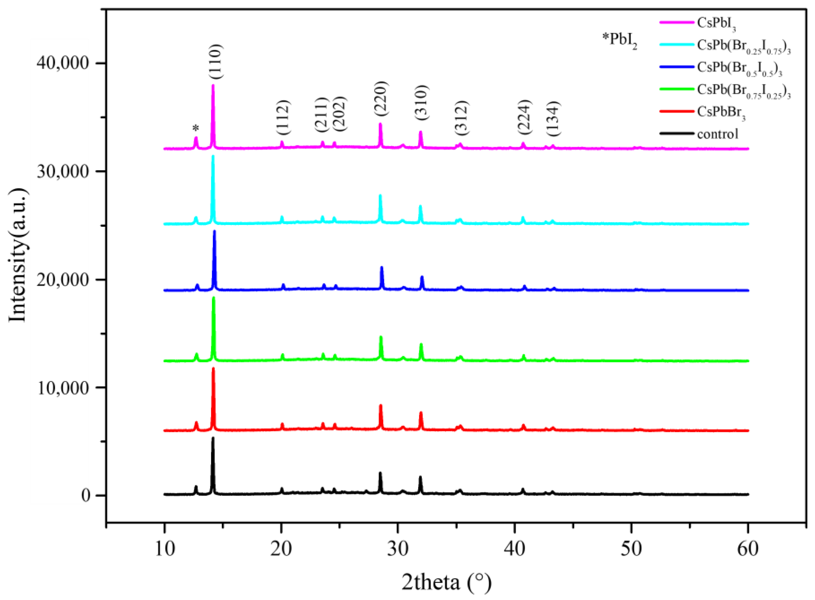
3.4. XRD Analysis
3.5. Absorption Spectrum
3.6. UPS and Energy Band Analysis
3.7. Photoluminescence Spectrum (PL)
3.8. TRPL Analysis
3.9. I-V/PCE and Lifetime Measurement
4. Conclusions
Author Contributions
Funding
Data Availability Statement
Conflicts of Interest
References
- Balanay, M.P.; Nirmala, R.; Kim, D.H.; Senthilkumar, N.; Kim, A.R.; Yoo, D.J. The photovoltaic performances of PVdF-HFP electrospun membranes employed quasi-solid-state dye sensitized solar cells. J. Nanosci. Nanotechnol. 2016, 16, 581–587. [Google Scholar]
- Senthilkumar, R.; Ramakrishnan, S.; Balu, M.; Batabyal, S.K.; Yoo, D.J.; Kumaresan, D.; Kothurkar, N.K. CoxMo1−x S2 intermixed reduced graphene oxide as efficient counter electrode materials for high-performance dye-sensitized solar cells. Int. J. Hydrogen Energy 2023, 48, 5901–5914. [Google Scholar] [CrossRef]
- Kojima, A.; Teshima, K.; Shirai, Y.; Miyasaka, T. Organometal Halide Perovskites as Visible-Light Sensitizers for Photovoltaic Cells. J. Am. Chem. Soc. 2009, 131, 6050–6051. [Google Scholar] [CrossRef] [PubMed]
- Aydin, E.; De Bastiani, M.; De Wolf, S. Defect and Contact Passivation for Perovskite Solar Cells. Adv. Mater. 2019, 31, e1900428. [Google Scholar] [CrossRef] [PubMed]
- Liu, Y.; Akin, S.; Pan, L.; Uchida, R.; Arora, N.; Milić, J.V.; Hinderhofer, A.; Schreiber, F.; Uhl, A.R.; Zakeeruddin, S.M.; et al. Ultrahydrophobic 3D:2D fluoroarene bilayer-based water-resistant perovskite solar cells with efficiencies exceeding 22. Sci. Adv. 2019, 5, eaaw2543. [Google Scholar] [CrossRef]
- Lu, J.; Jiang, L.; Li, W.; Li, F.; Pai, N.K.; Scully, A.D.; Tsai, C.; Bach, U.; Simonov, A.N.; Cheng, Y.; et al. Diammonium and Monoammonium Mixed-Organic-Cation Perovskites for High Performance Solar Cells with Improved Stability. Adv. Energy Mater. 2017, 7, 1700444. [Google Scholar] [CrossRef]
- Zhang, S.; Yoon, Y.J.; Cui, X.; Chang, Y.; Zhang, M.; Liang, S.; Lu, C.-H.; Lin, Z. Tailoring interfacial carrier dynamics via rationally designed uniform CsPbBrxI3−x quantum dots for high-efficiency perovskite solar cells. J. Mater. Chem. A 2020, 8, 26098–26108. [Google Scholar] [CrossRef]
- Huang, P.-H.; Chen, Y.-H.; Lien, S.-Y.; Lee, K.-W.; Wang, N.-F.; Huang, C.-J. Effect of Annealing on Innovative CsPbI3-QDs Doped Perovskite Thin Films. Crystals 2021, 11, 101. [Google Scholar] [CrossRef]
- Wang, P.; Xie, J.; Xiao, K.; Hu, H.; Cui, C.; Qiang, Y.; Lin, P.; Arivazhagan, V.; Xu, L.; Yang, Z.; et al. CH3NH3PbBr3 Quantum Dot-Induced Nucleation for High Performance Perovskite Light-Emitting Solar Cells. ACS Appl. Mater. Interfaces 2018, 10, 22320–22328. [Google Scholar] [CrossRef]
- Liu, X.Y. Heterogeneous nucleation or homogeneous nucleation? J. Chem. Phys. 2000, 112, 9949–9955. [Google Scholar] [CrossRef]
- Cacciuto, A.; Auer, S.; Frenkel, D. Onset of heterogeneous crystal nucleation in colloidal suspensions. Nature 2004, 428, 404–406. [Google Scholar] [CrossRef] [PubMed]
- Yao, Y.; Hang, P.; Wang, P.; Xu, L.; Cui, C.; Xie, J.; Xiao, K.; Li, G.; Lin, P.; Liu, S.; et al. CsPbBr3 quantum dots assisted crystallization of solution-processed perovskite films with preferential orientation for high performance perovskite solar cells. Nanotechnology 2019, 31, 085401. [Google Scholar] [CrossRef] [PubMed]
- Adinolfi, V.; Yuan, M.; Comin, R.; Thibau, E.S.; Shi, D.; Saidaminov, M.I.; Kanjanaboos, P.; Kopilovic, D.; Hoogland, S.; Lu, Z.; et al. The In-Gap Electronic State Spectrum of Methylammonium Lead Iodide Single-Crystal Perovskites. Adv. Mater. 2016, 28, 3406–3410. [Google Scholar] [CrossRef] [PubMed]
- Elumalai, N.K.; Uddin, A. Open circuit voltage of organic solar cells: An in-depth review. Energy Environ. Sci. 2015, 9, 391–410. [Google Scholar] [CrossRef]
- Yang, D.; Zhou, X.; Yang, R.; Yang, Z.; Yu, W.; Wang, X.; Li, C.; Liu, S.; Chang, R.P.H. Surface optimization to eliminate hysteresis for record efficiency planar perovskite solar cells. Energy Environ. Sci. 2016, 9, 3071–3078. [Google Scholar] [CrossRef]
- You, J.; Yang, Y.; Hong, Z.; Song, T.-B.; Meng, L.; Liu, Y.; Jiang, C.; Zhou, H.; Chang, W.-H.; Li, G. Moisture assisted perovskite film growth for high performance solar cells. Appl. Phys. Lett. 2014, 105, 183902. [Google Scholar] [CrossRef]
- Shi, D.; Adinolfi, V.; Comin, R.; Yuan, M.; Alarousu, E.; Buin, A.; Chen, Y.; Hoogland, S.; Rothenberger, A.; Katsiev, K.; et al. Low trap-state density and longcarrier diffusion in organoleadtrihalide perovskite single crystals. Science 2015, 347, 519–522. [Google Scholar] [CrossRef] [PubMed]
- Zhou, H.; Chen, Q.; Li, G.; Luo, S.; Song, T.-B.; Duan, H.-S.; Hong, Z.; You, J.; Liu, Y.; Yang, Y. Interface engineering of highly efficient perovskite solar cells. Science 2014, 345, 542–546. [Google Scholar] [CrossRef] [PubMed]
- Su, T.-S.; Eickemeyer, F.T.; Hope, M.A.; Jahanbakhshi, F.; Mladenović, M.; Li, J.; Zhou, Z.; Mishra, A.; Yum, J.-H.; Ren, D.; et al. Crown Ether Modulation Enables over 23% Efficient Formamidinium-Based Perovskite Solar Cells. J. Am. Chem. Soc. 2020, 142, 19980–19991. [Google Scholar] [CrossRef] [PubMed]
- Nie, W.; Tsai, H.; Asadpour, R.; Blancon, J.-C.; Neukirch, A.J.; Gupta, G.; Crochet, J.J.; Chhowalla, M.; Tretiak, S.; Alam, M.A.; et al. High-efficiency solution-processed perovskite solar cells with millimeter-scale grains. Science 2015, 347, 522–525. [Google Scholar] [CrossRef] [PubMed]


| Sample | Ra (nm) | Rms (nm) |
|---|---|---|
| control | 18.9 | 24.4 |
| CsPbBr3 | 14.5 | 18.4 |
| CsPb(Br0.75 I0.25)3 | 15.0 | 18.9 |
| CsPb(Br0.5 I0.5)3 | 13.8 | 17.4 |
| CsPb(Br0.25 I0.75)3 | 15.8 | 19.9 |
| CsPbI3 | 15.6 | 19.7 |
| Sample | MAPbI3(110) | PbI2(001) | MAPbI3(310) | (110)/(310) | MAPbI3(110)/ PbI2(001) |
|---|---|---|---|---|---|
| control | 5358 | 858 | 1741 | 3.08 | 6.245 |
| CsPbBr3 | 5503 | 868 | 1770 | 3.11 | 6.34 |
| CsPb(Br0.75 I0.25)3 | 5976 | 767 | 1655 | 3.61 | 7.791 |
| CsPb(Br0.5 I0.5)3 | 5568 | 605 | 1346 | 4.14 | 9.203 |
| CsPb(Br0.25 I0.75)3 | 6399 | 714 | 1782 | 3.59 | 8.962 |
| CsPbI3 | 5987 | 1147 | 1675 | 3.57 | 5.22 |
| Sample | A1 | (ns) | A2 | (ns) | |
|---|---|---|---|---|---|
| control | 0.83 | 22.7 | 0.43 | 133.9 | 106.4 |
| CsPb(Br0.5I0.5)3 | 0.27 | 29.1 | 0.27 | 241.4 | 218.5 |
| Sample | Jsc (mA/cm2) | Voc (V) | FF (%) | PCE (%) |
|---|---|---|---|---|
| control | 23.46 | 0.876 | 53.65 | 11.03 |
| CsPbBr3 | 23.48 | 0.907 | 0.55 | 11.64 |
| CsPb(Br0.75 I0.25)3 | 23.34 | 0.908 | 0.57 | 12.14 |
| CsPb(Br0.5 I0.5)3 | 23.48 | 0.915 | 0.60 | 12.88 |
| CsPb(Br0.25 I0.75)3 | 23.45 | 0.905 | 0.56 | 11.91 |
| CsPbI3 | 23.46 | 0.886 | 0.54 | 11.15 |
Disclaimer/Publisher’s Note: The statements, opinions and data contained in all publications are solely those of the individual author(s) and contributor(s) and not of MDPI and/or the editor(s). MDPI and/or the editor(s) disclaim responsibility for any injury to people or property resulting from any ideas, methods, instructions or products referred to in the content. |
© 2024 by the authors. Licensee MDPI, Basel, Switzerland. This article is an open access article distributed under the terms and conditions of the Creative Commons Attribution (CC BY) license (https://creativecommons.org/licenses/by/4.0/).
Share and Cite
Tsai, M.-C.; Chu, S.-Y.; Kao, P.-C. Performance Enhancement of Three-Dimensional MAPbI3 Perovskite Solar Cells by Doping Perovskite Films with CsPbX3 Quantum Dots. Materials 2024, 17, 1238. https://doi.org/10.3390/ma17061238
Tsai M-C, Chu S-Y, Kao P-C. Performance Enhancement of Three-Dimensional MAPbI3 Perovskite Solar Cells by Doping Perovskite Films with CsPbX3 Quantum Dots. Materials. 2024; 17(6):1238. https://doi.org/10.3390/ma17061238
Chicago/Turabian StyleTsai, Ming-Chen, Sheng-Yuan Chu, and Po-Ching Kao. 2024. "Performance Enhancement of Three-Dimensional MAPbI3 Perovskite Solar Cells by Doping Perovskite Films with CsPbX3 Quantum Dots" Materials 17, no. 6: 1238. https://doi.org/10.3390/ma17061238