
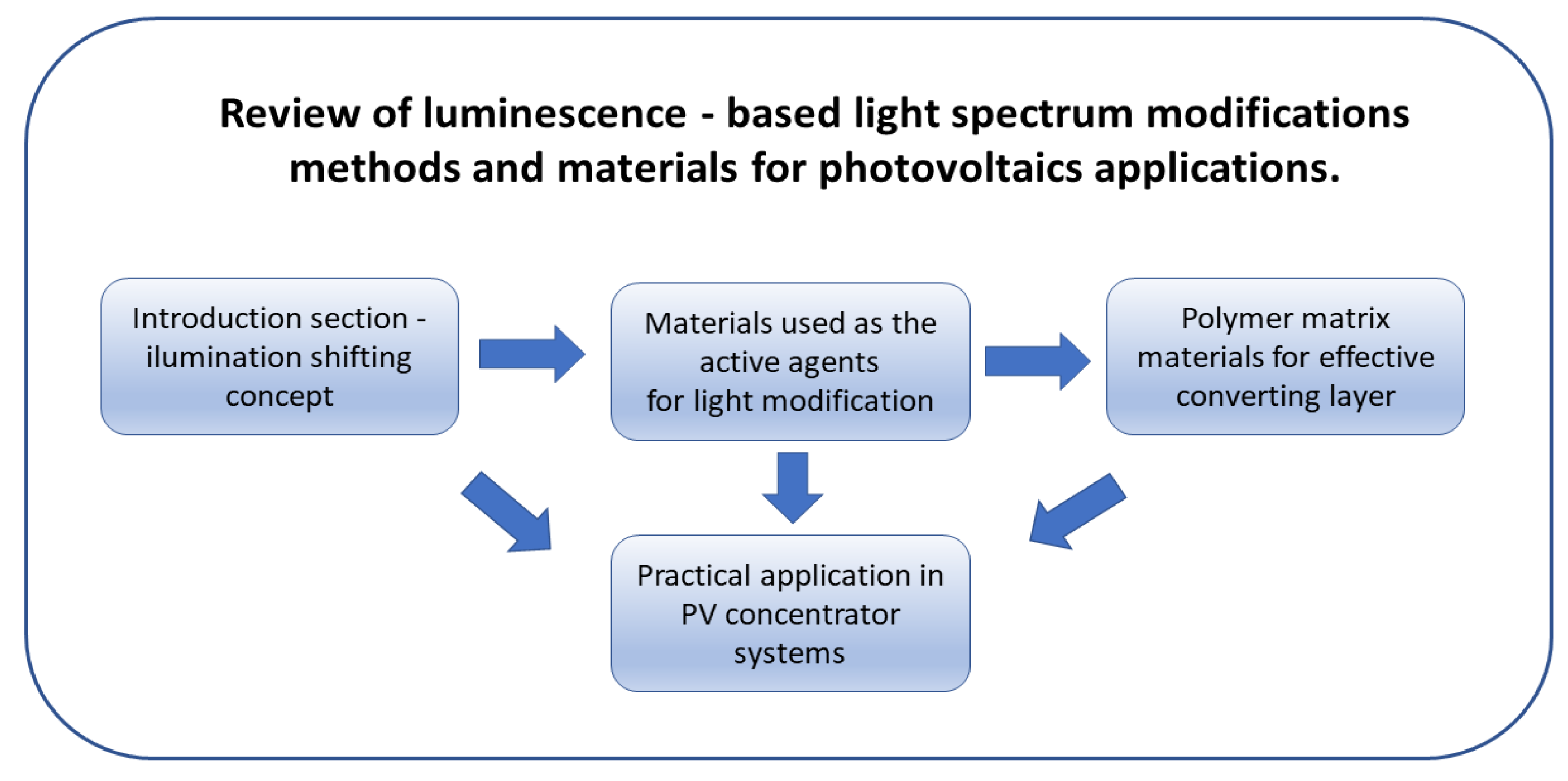
Review of Luminescence-Based Light Spectrum Modifications Methods and Materials for Photovoltaics Applications


Abstract
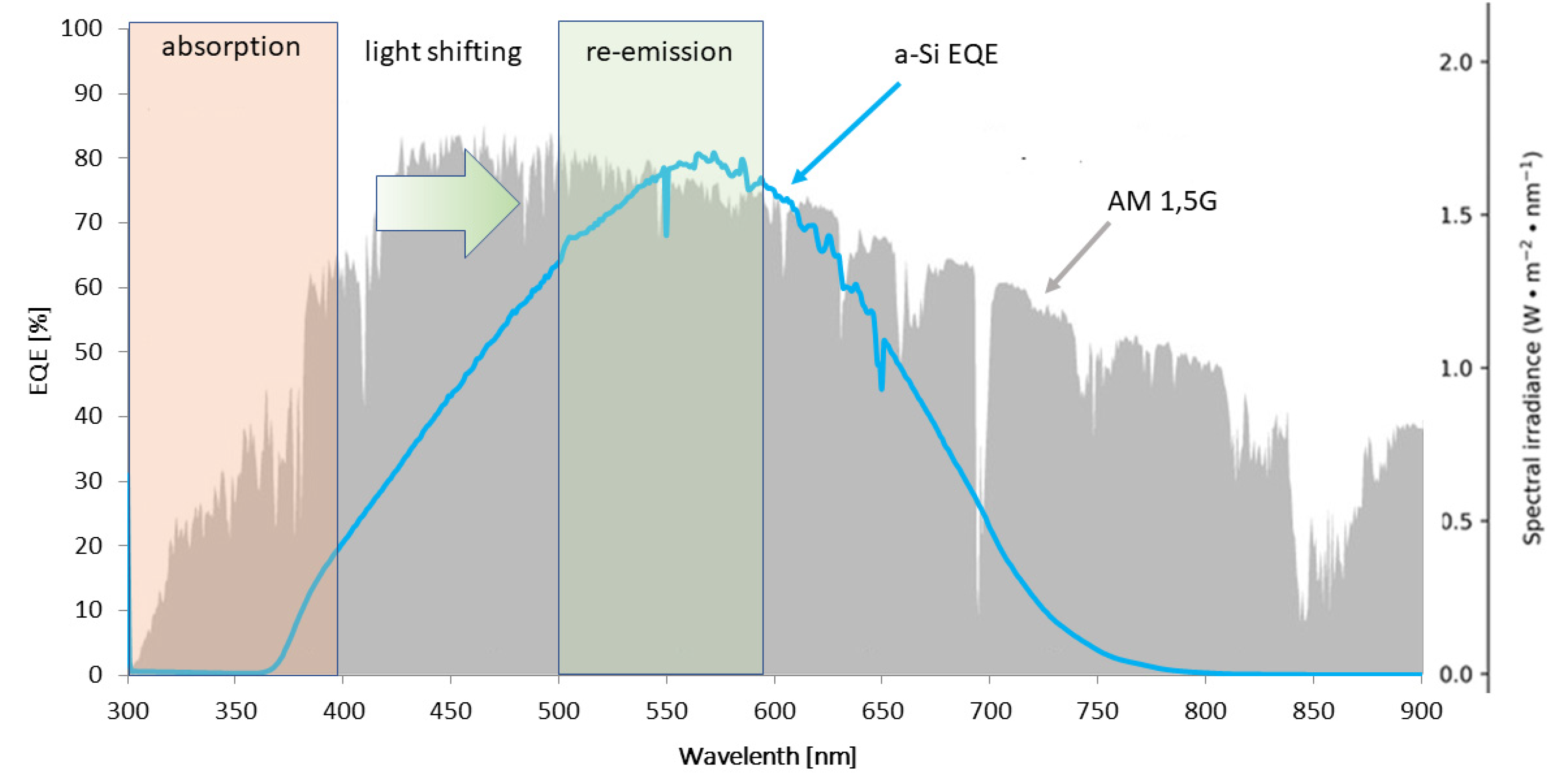
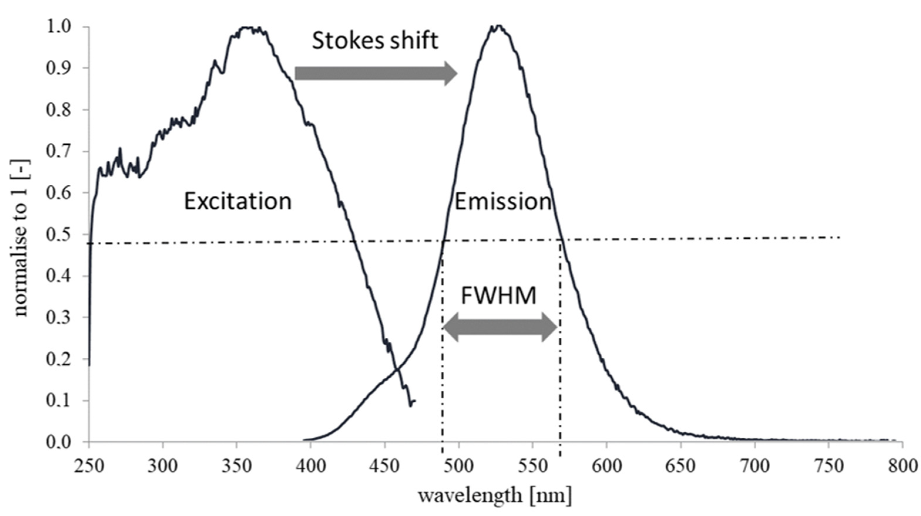
:1. Luminescence Mechanisms and Their Utilization in Photovoltaics
1.1. Down Conversion by Metal Oxides-ZnO Nanoparticles
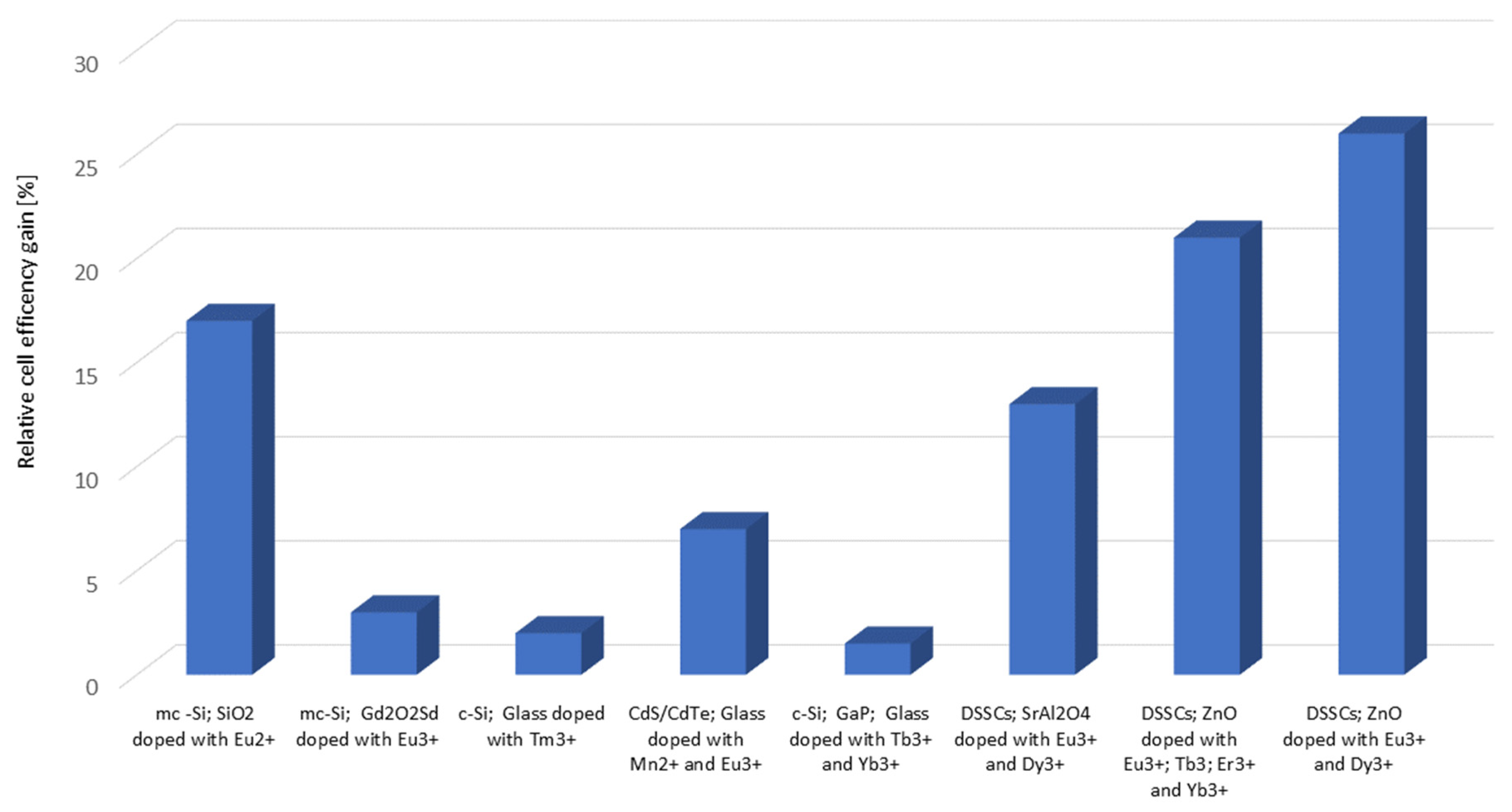
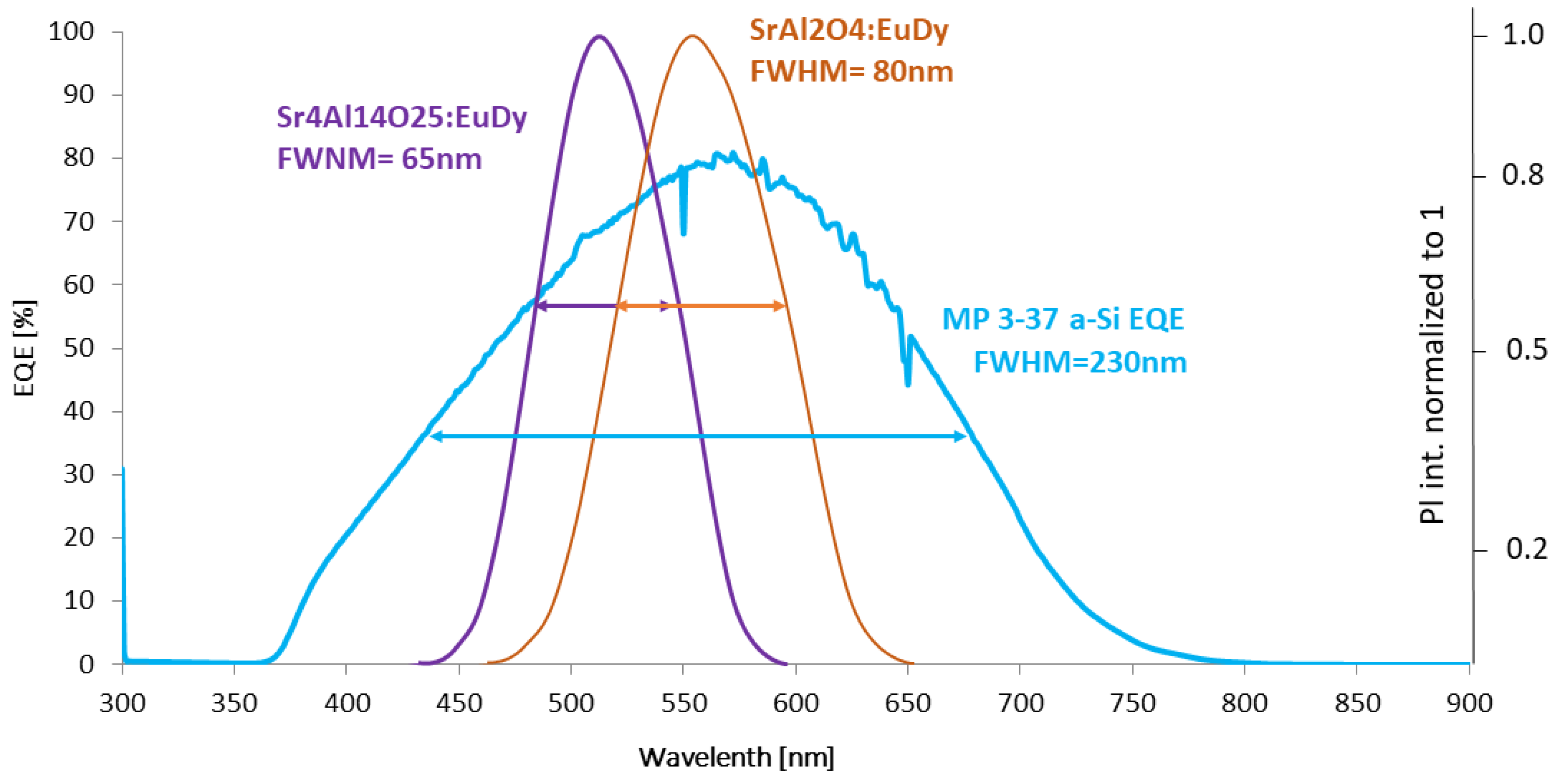
1.2. Rare Earth Elements and Other Inorganic Materials for Luminescent Spectrum Modifications
1.3. Organic Luminophores
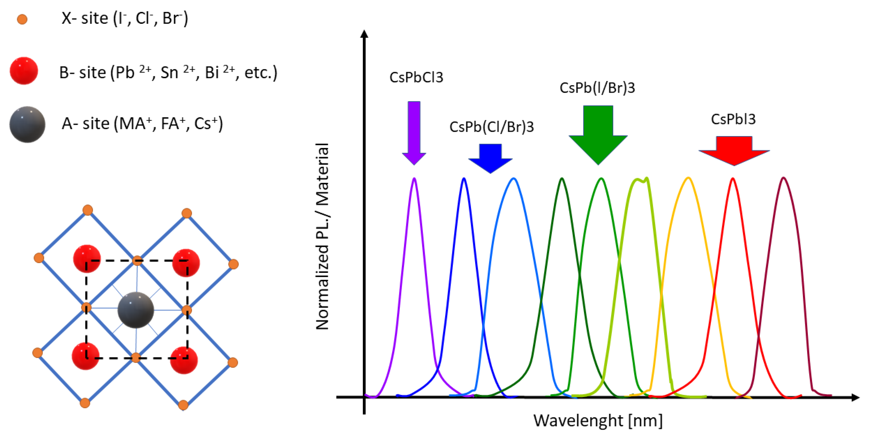
1.4. Quantum Dots and Perovskites in Luminescent Applications
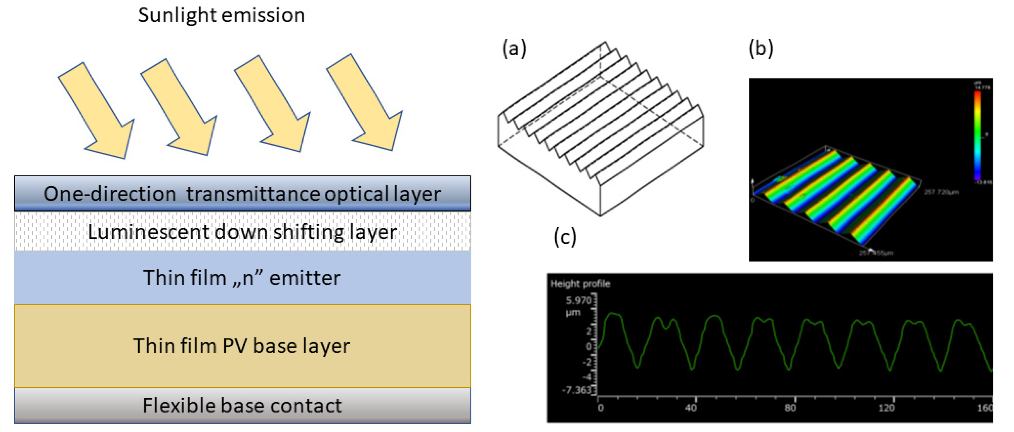
2. Carrier Matrix Material and Converting Layer Preparation
- The good optical transparency in the UV-Vis spectrum;
- The appropriate refractive index for incoming light reflection reduction and total internal reflection creation;
- An easy method of luminescent compound dispersion;
- The non-suppressive character of the luminescent compound emission effect;
- The strong adhesion to dedicated substrates;
- The possibility of a flexible structure;
- The cheap and scalable method of deposition.
- Dip coating;
- Spin coating;
- Spray coating;
- Printing technologies.
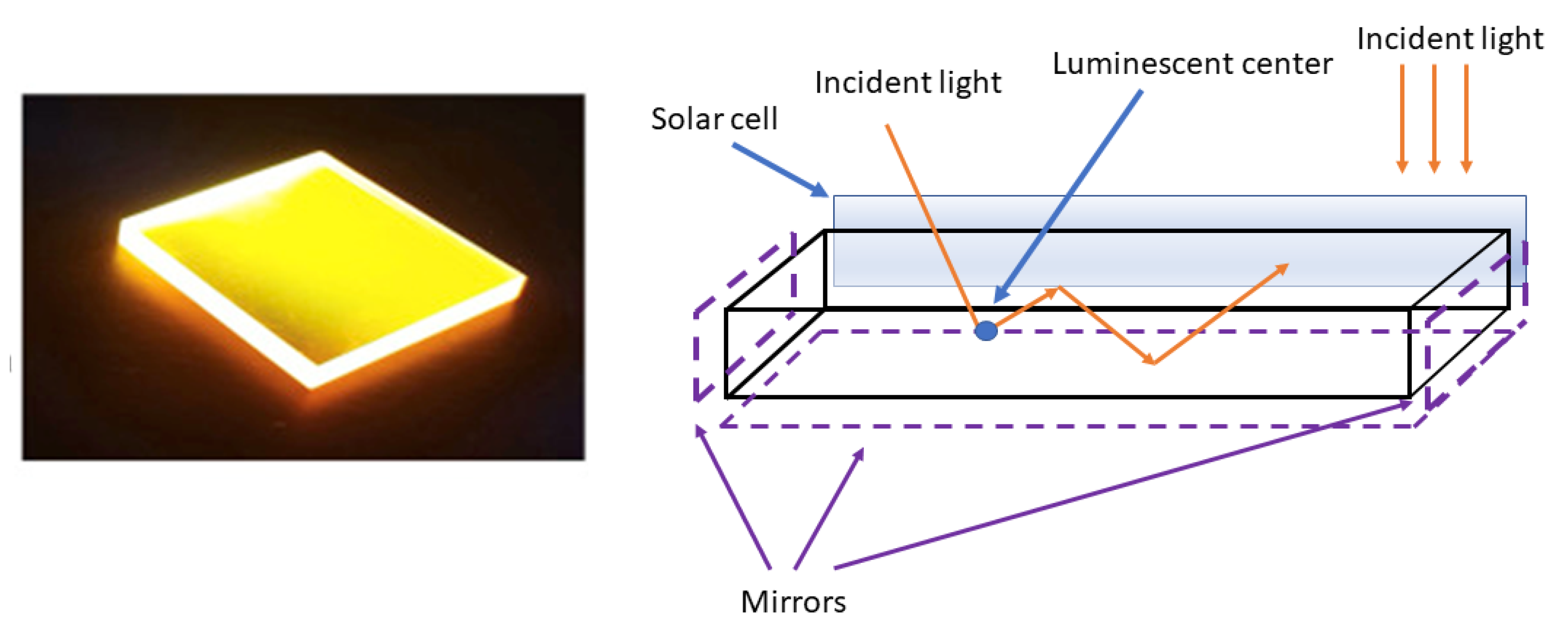
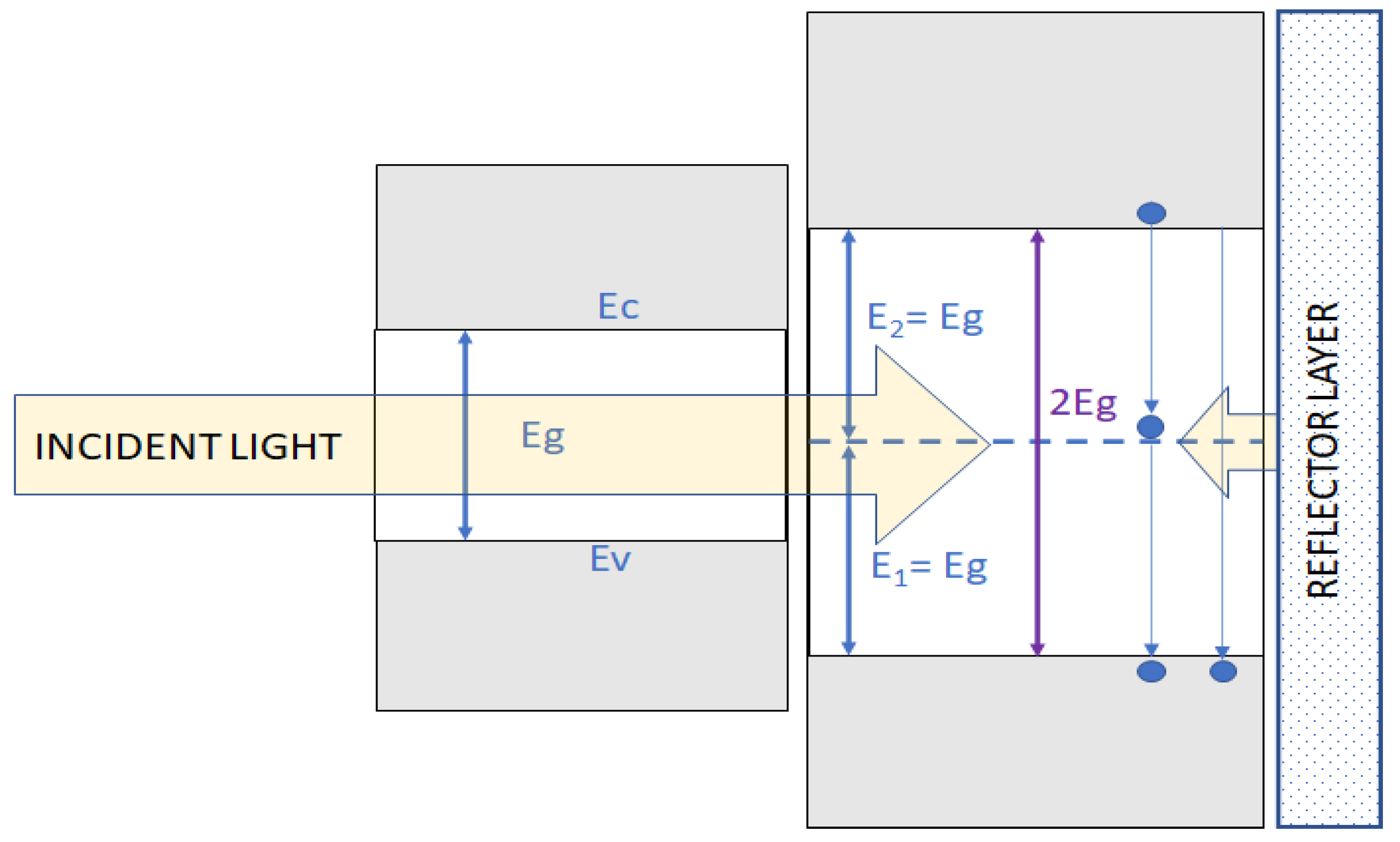
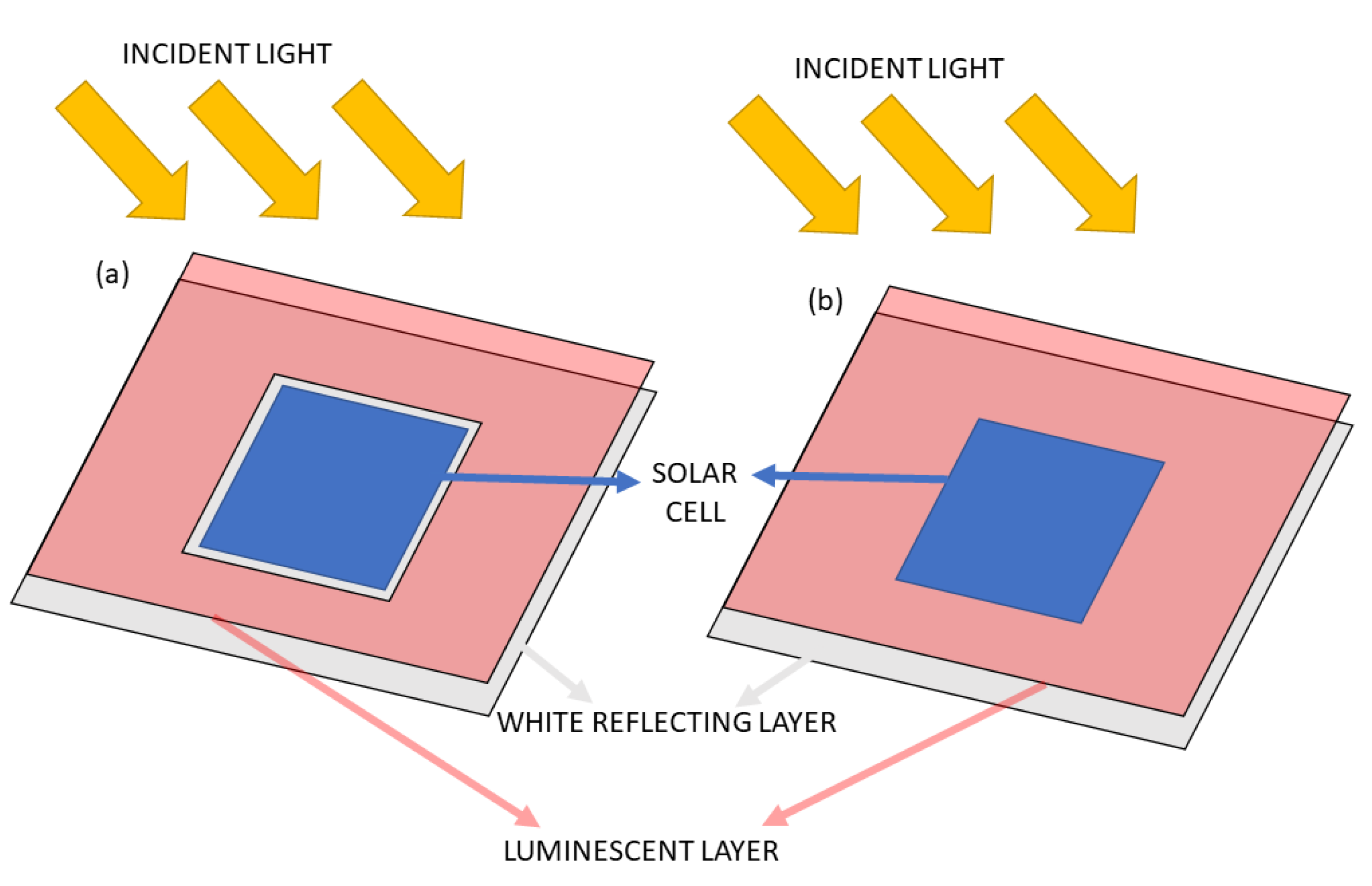
3. Application in LSC (Luminescent Solar Concentrator) Systems
4. Conclusions
Funding
Institutional Review Board Statement
Informed Consent Statement
Data Availability Statement
Conflicts of Interest
References
- Murthy, K.V.R.; Virk, H.S. Luminescence Phenomena: An Introduction. Defect Diffus. Forum 2014, 347, 1–34. [Google Scholar] [CrossRef]
- Goldberg, P. (Ed.) Luminescence of Inorganic Solids; Academic, Press: New York, NY, USA; London, UK, 1966. [Google Scholar]
- Blasse, G.; Grabmaier, B.C. Luminescent Materials; Springer: Berlin/Heidelberg, Germany, 1994. [Google Scholar]
- Richards, B.S. Luminescent layers for enhanced silicon solar cell performance: Down-conversion. Sol. Energy Mater. Sol. Cells 2006, 90, 1189–1207. [Google Scholar] [CrossRef]
- Rao, A.; Friend, R.H. Harnessing singlet exciton fission to break the Shockley–Queisser limit. Nat. Rev. Mater. 2017, 2, 17063. [Google Scholar] [CrossRef]
- Day, J.; Senthilarasu, S.; Mallick, T.K. Improving spectral modification for applications in solar cells: A review. Renew. Energy 2019, 132, 186–205. [Google Scholar] [CrossRef]
- Shockey, W.; Queisser, H.J. Detailed balance limit of efficiency of p-n junction solar cells. J. Appl. Phys. 1961, 32, 510–519. [Google Scholar] [CrossRef]
- Green, M.; Dunlop, E.; Hohl-Ebinger, J.; Yoshita, M.; Kopidakis, N.; Hao, X. Solar cell efficiency tables (version 57). Prog. Photovolt. Res. Appl. 2021, 29, 3–15. [Google Scholar] [CrossRef]
- Alharbi, F.H.; Kais, S. Theoretical limits of photovoltaics efficiency and possible improvements by intuive approaches learned from photosynthesis and quantum coherence. Renew. Sustain. Energy Rev. 2015, 43, 1073–1089. [Google Scholar] [CrossRef] [Green Version]
- Luque, A.; Martí, A. Increasing the Efficiency of Ideal Solar Cells by Photon Induced Transitions at Intermediate Levels. Phys. Rev. Lett. 1997, 78, 5014. [Google Scholar] [CrossRef]
- Kahmann, S.; Loi, M.A. Hot carrier solar cells and the potential of perovskites for breaking the Shockley–Queisser limit. J. Mater. Chem. C 2019, 7, 2471–2486. [Google Scholar] [CrossRef] [Green Version]
- Delerue, C.; Allan, G.; Pijpers, J.J.H.; Bonn, M. Carrier multiplication in bulk and nanocrystalline semiconductors: Mechanism, efficiency, and interest for solar cells. Phys. Rev. B 2010, 81, 125306. [Google Scholar] [CrossRef]
- Bierman, D.M.; Lenert, A.; Wang, E.N. Spectral splitting optimization for high-efficiency solar photovoltaic and thermal power generation. Appl. Phys. Lett. 2016, 109, 243904. [Google Scholar] [CrossRef]
- Klampaftis, E.; Ross, D.; McIntosh, K.R.; Richards, B.S. Enhancing the performance of solar cells via luminescent down-shifting of incident spectrum: A review. Sol. Energy Mater. Sol. Cells 2009, 93, 1182–1194. [Google Scholar] [CrossRef]
- Stanley, C.; Mojiri, A.; Rosengarten, G. Spectral light management for solar energy conversion systems. Nanophotonics 2016, 5, 161–179. [Google Scholar] [CrossRef]
- Hovel, H.J.; Hodgson, R.T.; Woodall, J.M. The effect of fluorescent wavelength shifting on solar cell spectral response. Sol. Energy Mater. 1979, 2, 19–29. [Google Scholar] [CrossRef]
- Weber, W.H.; Lambe, J. Luminescent Collector for Solar Radiation. Appl. Opt. 1976, 15, 2299–2300. [Google Scholar] [CrossRef]
- Levitt, J.A.; Weber, W.H. Materials for Luminescent Greenhouse Solar Collectors. Appl. Opt. 1977, 16, 2684–2689. [Google Scholar] [CrossRef]
- Van Sark, W.G.; AMeijerink, A.; Schropp, R.E.I.; Van Roosmalen, J.A.M.; Lysen, E.H. Enhancing solar cell efficiency by using spectral converters. Sol. Energy Mater. Sol. Cells 2005, 87, 395–409. [Google Scholar] [CrossRef] [Green Version]
- Gabr, A.M.; Walker, A.; Wilkins, M.M.; Kleiman, R.N.; Hinzer, K. Procedure to decouple reflectance and downshifting effects in luminescent down-shifting enhanced photovoltaics. Opt. Express 2017, 25, 530–538. [Google Scholar] [CrossRef] [PubMed] [Green Version]
- De la Mora, M.B.; Amelines-Sarria, O.; Monroy, B.M.; Hernandez, C.D.; Lugo, J.E. Materials for downconversion in solar cells: Perspectives and challenges. Sol. Energy Mater. Sol. Cells 2017, 165, 59–71. [Google Scholar] [CrossRef]
- Florencio, L.A.; Gomez-Malagon, L.A.; Lima, B.C.; Gomes, A.S.L.; Garcia, J.A.M.; Kassab, L.R.P. Efficiency enhancement in solar cells using photon down-conversion in Tb/Yb-doped tellurite glass. Sol. Energy Mater. Sol. Cells 2016, 157, 468–475. [Google Scholar] [CrossRef] [Green Version]
- Portier, J.; Hilal, H.S.; Saadeddin, I.; Hwang, S.J.; Subramanian, M.A.; Campet, G. Thermodynamic correlations and band gap calculations in metal oxides. Prog. Solid State Chem. 2004, 32, 207–217. [Google Scholar] [CrossRef]
- Tsukazaki, A.; Ohtomo, A.; Onuma, T.; Ohtani, M.; Makino, T.; Sumiya, M.; Ohtani, K.; Chichibu, S.F.; Fuke, S.; Kawasaki, M.; et al. Repeated temperature modulation epitaxy for p-type doping and lightemitting diode based on ZnO. Nat. Mater. 2005, 4, 42–45. [Google Scholar] [CrossRef]
- Coleman, V.A.; Jagadish, C. Zinc Oxide Bulk, Thin Films and Nanostructures; Elsevier Science: London, UK, 2006. [Google Scholar]
- Wong, T.K.; Zhuk, S.; Masudy-Panah, S.; Dalapati, G.K. Current status and future prospects of copper oxide heterojunction solar cells. Materials 2016, 9, 271. [Google Scholar] [CrossRef]
- Sibiński, M.; Znajdek, K.; Walczak, S.; Słoma, M.; Górski, M.; Cenian, A. Comparison of ZnO:Al, ITO and carbon nanotube transparent conductive layers in flexible solar cells applications. Mater. Sci. Eng. B Solid-State Mater. Adv. Technol. 2012, 177, 1292–1298. [Google Scholar] [CrossRef]
- Zhang, L.; Che, Z.; Shang, J.; Wang, Q.; Cao, M.; Zhou, Y.; Zhou, Y.; Liu, F. Cerium-Doped Indium Oxide as a Top Electrode of Semitransparent Perovskite Solar Cells. ACS Appl. Mater. Interfaces 2023, 15, 10838–10846. [Google Scholar] [CrossRef]
- Yang, Y.J.; Li, J.H.; Jianming, Y.; Bin, S.; Qinye, B.; Zheng, T.; Zaifei, M. ITO Electrode with a Tunable Work Function for Organic Photovoltaic Devices. ACS Appl. Electron. Mater. 2022, 4, 4104–411223. [Google Scholar] [CrossRef]
- Alivisatos, A.P. Semiconductor clusters, nanocrystals, and quantum dots. Science 1996, 271, 933–937. [Google Scholar] [CrossRef] [Green Version]
- Stankic, S.; Suman, S.; Haque, F.; Vidic, J. Pure and multi metal oxide nanoparticles: Synthesis, antibacterial and cytotoxic properties. J. Nanobiotechnology 2016, 14, 73. [Google Scholar] [CrossRef] [PubMed] [Green Version]
- Ren, Y.; Liu, Z.; Pourpoint, F.; Armstrong, A.R.; Grey, C.P.; Bruce, P.G. Nanoparticulate TiO2(B): An anode for lithium-ion batteries. Angew. Chem. Int. Ed. 2012, 51, 2164–2167. [Google Scholar] [CrossRef] [PubMed]
- Altavilla, C.; Ciliberto, E. (Eds.) Inorganic Nanoparticles; CRC Press: Boca Raton, FL, USA, 2011. [Google Scholar]
- Thiagarajan, S.; Sanmugam, A.; Vikraman, D. Facile Methodology of Sol-Gel Synthesis for Metal Oxide Nanostructures. In Recent Applications in Sol-Gel Synthesis; IntechOpen: London, UK, 2017; pp. 1–16. [Google Scholar]
- Aghababazadeh, R.; Mazinani, B.; Mirhabibi, A.; Tamizifar, M. ZnO Nanoparticles Synthesised by mechanochemical processing. J. Phys. Conf. Ser. 2006, 26, 312–314. [Google Scholar] [CrossRef] [Green Version]
- Casey, P. Nanoparticle technologies and applications. In Nanostructure Control of Materials; Woodhead Publishing: Cambridge, UK, 2006; pp. 1–31. [Google Scholar]
- Apostoluk, A.; Masenelli, B.; de Lyon, I.E.A.A.d.N.; Canut, B.; Hapiuk, D.; Mélinon, P.; Delaunay, J.-J.; Liu, N.; Xu, L.; Wang, H.; et al. Efficient ultraviolet light frequency down-shifting by a thin film of ZnO nanoparticles. Int. J. Nanotechnol. 2012, 11, 1240022. [Google Scholar] [CrossRef]
- Huotari, J.; Lappalainen, J.; Puustinen, J.; Baur, T.; Alépée, C.; Haapalainen, T.; Komulainen, S.; Pylvänäinen, J.; Spetz, A.L. Pulsed Laser Deposition of Metal Oxide Nanoparticles, Agglomerates, and Nanotrees for Chemical Sensors. Procedia Eng. 2015, 120, 1158–1161. [Google Scholar] [CrossRef] [Green Version]
- Özgür, U.; Alivov, Y.I.; Liu, C.; Teke, A.; Reshchikov, M.A.; Doğan, S.; Avrutin, V.; Cho, S.J.; Morkoç, H. A comprehensive review of ZnO materials and devices. Appl. Phys. 2005, 98, 103. [Google Scholar] [CrossRef] [Green Version]
- Dong, H.X.; Liu, Y.; Lu, J.; Chen, Z.H.; Wang, J.; Zhang, L. Single-crystalline tower-like ZnO microrod UV lasers. J. Mater. Chem. C 2013, 1, 202–206. [Google Scholar] [CrossRef]
- Liu, K.; Sakurai, M.; Aono, M. ZnO-based ultraviolet photodetectors. Sensors 2010, 10, 8604–8634. [Google Scholar] [CrossRef] [Green Version]
- Park, S.; Ikegami, T.; Ebihara, K. Effects of substrate temperature on the properties of Ga-doped ZnO by pulsed laser deposition. Thin Solid Film. 2006, 513, 90–94. [Google Scholar] [CrossRef]
- Ramanathan, K.; Contreras, M.A.; Perkins, C.L.; Asher, S.; Hasoon, F.S.; Keane, J.; Young, D.; Romero, M.; Metzger, W.; Noufi, R.; et al. Properties of 19.2% efficiency ZnO/CdS/CuInGaSe2 thin-film solar cells. Prog. Photovolt. Res. Appl. 2003, 11, 225–230. [Google Scholar] [CrossRef]
- White, M. Production and Analysis of Conjugate Polymer/ZnO Solar Cells. NNIN REU Res. Accompl. 2005, 156–157. [Google Scholar]
- Zin, Z.C.; Hamberg, I.; Granqvist, C.G. Optical properties of sputter-deposited ZnO:Al thin films. J. Appl. Phys. 1988, 64, 5117–5131. [Google Scholar]
- Lee, Y.-J.; Ruby, D.S.; Peters, D.W.; McKenzie, B.B.; Hsu, J.W.P. ZnO nanostructures as efficient antireflection layers in solar cells. Nano Lett. 2008, 8, 1501–1505. [Google Scholar] [CrossRef] [PubMed]
- Vinod, R.; Sajan, P.; Achary, S.R.; Tomas, C.M.; Muñoz-Sanjosé, V.; Bushiri, M.J. Enhanced UV emission from ZnO nanoflowers synthesized by the hydrothermal process. J. Phys. D Appl. Phys. 2012, 45, 425103. [Google Scholar] [CrossRef]
- Richters, J.P.; Voss, T.; Wischmeier, L.; Ruckmann, I.; Gutowski, J. Near-band-edge photoluminescence spectroscopy of ZnO nanowires embedded in polymers. J. Korean Phys. Soc. 2008, 53, 2844–2846. [Google Scholar] [CrossRef]
- Samanta, P.K.; Patra, S.K.; Ghosh, A.; Chaudhuri, P.R. Visible emission from ZnO nanorods synthesized by a simple wet chemical method. Int. J. Nanosci. Nanotechnol. 2009, 1, 81–90. [Google Scholar]
- Xiao, Y.L.W.; Xue, W.; Li, J.; Ding, J. Controllable synthesis of ZnO nanoparticles with high intensity visible photoemission and investigation of its mechanism. Nanotechnology 2013, 24, 175702. [Google Scholar]
- Apostoluk, A.; Zhu, Y.; Canut, B.; Masenelli, B.; Delaunay, J.-J.; Znajdek, K.; Sibiński, M. Investigation of luminescent properties of ZnO nanoparticles for their use as a down-shifting layer on solar cells. Phys. Status Solidi (C) Curr. Top. Solid State Phys. 2013, 2, 1301–1307. [Google Scholar] [CrossRef]
- Bano, N.; Zaman, S.; Zainelabdin, A.; Hussain, S.; Hussain, I.; Nur, O.; Willander, M. ZnO-organic hybrid white light emitting diodes grown on flexible plastic using low temperature aqueous chemical method. J. Appl. Phys. 2010, 108, 043103. [Google Scholar] [CrossRef] [Green Version]
- Baruah, S.; Sinha, S.S.; Ghosh, B.; Pal, S.K.; Raychaudhuri, A.K.; Dutta, J. Photoreactivity of ZnO nanoparticles in visible light: Effect of surface states on electron transfer reaction. J. Appl. Phys. 2009, 105, 074308. [Google Scholar] [CrossRef] [Green Version]
- Apostoluk, A.; Zhu, Y.; Masenelli, B.; Delaunay, J.J.; Sibiński, M.; Znajdek, K.; Focsa, A.; Kaliszewska, I. Improvement of the solar cell efficiency by the ZnO nanoparticle layer via the down-shifting effect. Microelectron. Eng. 2014, 127, 51–56. [Google Scholar] [CrossRef]
- Morales-Flores, N.; Galeazzi, R.; Rosendo, E.; Díaz, T.; Velumani, S.; Pal, U. Morphology control and optical properties of ZnO nanostructures grown by ultrasonic synthesis. Adv. Nano Res. 2013, 1, 59–70. [Google Scholar] [CrossRef]
- Znajdek, K.; Sibiński, M.; Lisik, Z.; Apostoluk, A.; Zhu, Y.; Masenelli, B.; Sędzicki, P. Zinc oxide nanoparticles for improvement of thin film photovoltaic structures’ efficiency through down shifting conversion. Opto-Electron. Rev. 2017, 25, 99–102. [Google Scholar] [CrossRef]
- Baruah, S.; Dutta, J. Hydrothermal growth of ZnO nanostructures. Sci. Technol. Adv. Mater. 2009, 10, 18. [Google Scholar] [CrossRef]
- Rania, S.; Surib, P.; Shishodiac, P.K.; Mehra, R.M. Synthesis of nanocrystalline ZnO powder via sol–gel route for dye-sensitized solar cells. Sol. Energy Mater. Sol. Cells 2008, 92, 1639–1645. [Google Scholar] [CrossRef]
- Zhang, Y.; Gard, T.; Theron, C.; Apostoluk, A.; Masenelli-Varlot, L.; Canut, B.; Danielle, S.; Masenelli, B. Visible luminescence improvement of ZnO/PAA nano-hybrids by silica coating. Appl. Surf. Sci. 2021, 540, 148343. [Google Scholar] [CrossRef]
- Djurišić, A.B.; Leung, Y.H. Optical properties of ZnO nanostructures. Small 2006, 2, 944–961. [Google Scholar] [CrossRef]
- McCluskey, M.D.; Jokela, S.J. Defects in ZnO. J. Appl. Phys. 2009, 106, 13. [Google Scholar] [CrossRef] [Green Version]
- Sakirzanovas, S. Novel Sm2+/Sm3+ Phosphors as luminescence converter for Near UV Radiation. Ph.D. Thesis, Vilnius University, Vilna, Lithuania, 2011. [Google Scholar]
- Balaram, V. Rare earth elements: A review of applications, occurrence, exploration, analysis, recycling, and environmental impact. Geosci. Front. 2019, 10, 1285–1303. [Google Scholar] [CrossRef]
- Dorenbos, P. Electronic structure engineering of lanthanide activated materials. J. Mater. Chem. 2012, 2012, 22344. [Google Scholar] [CrossRef]
- Werts, M. Making sense of lanthanide luminescence. Sci. Prog. 2005, 88 Pt 2, 101–131. [Google Scholar] [CrossRef] [PubMed]
- Strumpel, C.; McCann, M.; Beaucarne, G.; Arkhipov, V.; Slaoui, A.; Svrcek, V.; Del Canizo, C.; Tobias, I. Modifying the solar spectrum to enhance silicon solar cell efficiency-An overview of available materials. Sol. Energy Mater. Sol. Cells 2007, 91, 238–249. [Google Scholar] [CrossRef]
- Hung, W.B.; Chen, T.M. Efficiency enhancement of silicon solar cells through a downshifting and antireflective oxysulfide phosphor layer. Sol. Energy Mater. Sol. Cells 2015, 133, 39–47. [Google Scholar] [CrossRef]
- Ho, W.J.; Shen, Y.T.; Deng, Y.J.; Yeh, C.W.; Sue, R.S. Performance enhancement of planar silicon solar cells through utilization of two luminescent downshifting Eu-doped phosphor species. Thin Solid Film. 2016, 618, 141–145. [Google Scholar] [CrossRef]
- Maalej, O.; Merigeon, J.; Boulard, B.; Girtan, M. Visible to near-infrared downshifting in Tm3+ doped fluoride glasses for solar cells efficiency enhancement. Opt. Mater. 2016, 60, 235–239. [Google Scholar] [CrossRef]
- Song, P.; Zhang, C.; Zui, P. Eu3+-Mn2+-doped bi-functional glasses with solar photon downshifting: Application to CdS/CdTe solar cells. J. Alloys Compd. 2016, 661, 14–19. [Google Scholar] [CrossRef]
- Yao, N.; Huang, J.; Deng, K.F.X.; Ding, M.; Shao, M.; Xu, X. Enhanced light harvesting of dye-sensitized solar cells with up/down conversion materials. Electrochim. Acta 2015, 154, 273–277. [Google Scholar] [CrossRef]
- Znajdek, K.; Szczecinska, N.; Sibinski, M.; Czarnecki, P.; Wiosna-Sałyga, G.; Apostoluk, A.; Mandrolo, F.; Rogowski, S.; Lisik, Z. Energy converting layers for thin-film flexible photovoltaic structures. Open Phys. 2018, 16, 820–825. [Google Scholar] [CrossRef]
- Znajdek, K.; Gwardjan, N.; Sosna-Głębska, A.; Sibiński, M. Spray Coating Luminescence Layers on Glass for Si Solar Cells Efficiency Enhancement. Energies 2021, 14, 6884. [Google Scholar] [CrossRef]
- Sun, H.; Pan, L.; Zhu, G.; Piao, X.; Zhang, L.; Sun, Z. Long afterglow Sr4Al14O25:Eu,Dy phosphors as both scattering and down converting layer for CdS quantum dot-sensitized solar cells. Dalton Trans. 2014, 43, 14936–14941. [Google Scholar] [CrossRef] [PubMed]
- Nowsherwan, G.A.; Samad, A.; Iqbal, M.A.; Mushtaq, T.; Hussain, A.; Malik, M.; Haider, S.; Pham, P.V.; Choi, J.R. Performance Analysis and Optimization of a PBDB-T:ITIC Based Organic Solar Cell Using Graphene Oxide as the Hole Transport Layer. Nanomaterials 2022, 12, 1767. [Google Scholar] [CrossRef] [PubMed]
- Nemoto Lumi-materials Co., LTD. Phosphorescent Pigments Characterization. Available online: https://nemoto.co.jp/images/nlm/luminova/PDF/LumiNovaBG2015Mar.pdf (accessed on 20 January 2017).
- Znajdek, K.; Szczecińska, N.; Sibiński, M.; Wiosna-Sałyga, G.; Przymęcki, K. Luminescent layers based on rare earth elements for thin-film flexible solar cells applications. Optik 2018, 165, 200–209. [Google Scholar] [CrossRef]
- Sobik, P.; Jeremiasz, O.; Nowak, P.; Sala, A.; Pawłowski, B.; Kulesza-Matlak, G.; Sypień, A.; Drabczyk, K. Towards efficient luminescent solar energy concentrator using cuprorivaite infrared phosphor (Cacusi4o10)—Effect of dispersing method on photoluminescence intensity. Materials 2021, 14, 3952. [Google Scholar] [CrossRef]
- Li, Y.J.; Ye, S.; Wang, C.H.; Wang, X.M.; Zhang, Q.Y. Temperature-dependent near-infrared emission of highly concentrated Cu2+ in CaCuSi4O10 phosphor. J. Mater. Chem. C 2014, 2, 10395–10402. [Google Scholar] [CrossRef]
- Ko, D.H.; Tumbleston, J.R.; Zhang, L.; Williams, S.; DeSimone, J.; Lopez, R.; Samulski, E. Photonic Crystal Geometry for Organic Solar Cells. Nano Lett. 2009, 9, 2742–2746. [Google Scholar] [CrossRef]
- Peng, W.; Lin, Y.; Jeong, S.Y.; Genene, Z.; Magomedov, A.; Woo, H.Y.; Chen, C.; Wahyudi, W.; Tao, Q.; Deng, J.; et al. Over 18% ternary polymer solar cells enabled by a terpolymer as the third component. Nano Energy 2022, 92, 106681. [Google Scholar] [CrossRef]
- Ren, H.; De Chen, J.; Li, Y.-Q.; Tang, J.-X. Recent Progress in Organic Photodetectors and their Applications. Adv. Sci. 2020, 8, 2002418. [Google Scholar] [CrossRef] [PubMed]
- Li, J.; Xie, J.; Zhang, R.; Guo, S.; Zhang, F.; Guo, K.; Dong, S. Metal-free organic luminophores with ultrastrong dipole moment exhibiting force-induced near-infrared emission (>800 nm) turn-on. Chem. Commun. Issue 2018, 81, 11455–11458. [Google Scholar] [CrossRef] [PubMed]
- Shimizu, M.; Sakurai, T. Metal-Free Organic Luminophores that Exhibit Dual Fluorescence and Phosphorescence Emission at Room Temperature. ChemPlusChem 2021, 86, 446–459. [Google Scholar] [CrossRef]
- Sobik, P. New Luminescent Solar Concentrators for Packaging Processes in Photovoltaic Modules. Ph.D. Thesis, Institute of Metallurgy and Materials Science, Polish Academy of Sciences, Cracow, Poland, 2021. [Google Scholar]
- Slooff, L.H.; Bende, E.E.; Burgers, A.R.; Budel, T.; Pravettoni, M.; Kenny, R.; Dunlop, E.; Büchtemann, A. A luminescent solar concentrator with 7.1% power conversion efficiency. Phys. Status Solidi (RRL)—Rapid Res. Lett. 2008, 2, 257–259. [Google Scholar] [CrossRef] [Green Version]
- Griffini, G.; Brambilla, L.; Levi, M.; Del Zoppo, M.; Turri, S. Photo-degradation of a Perylene-based organic luminescent solar concentrator: Molecular aspects and device implications. Sol. Energy Mater. Sol. Cells 2013, 111, 41–48. [Google Scholar] [CrossRef]
- Schreiber, U. Chlorophyll fluorescence yield changes as a tool in plant physiology I. The measuring system. Photosynth. Res. 1983, 4, 361–373. [Google Scholar] [CrossRef]
- Nan, H.; Shen, H.P.; Wang, G.; Xie, S.D.; Yang, G.J.; Lin, H. Studies on the optical and photoelectric properties of anthocyanin and chlorophyll as natural co-sensitizers in dye sensitized solar cell. Opt. Mater. 2017, 73, 172–178. [Google Scholar] [CrossRef]
- Wang, S.H.; Duan, S.N.; Wang, Y.W.; Sun, C.L.; Wang, X.F.; Sasaki, S. Chlorophyll-based organic solar cells with improved power conversion efficiency. J. Energy Chem. 2019, 38, 88–93. [Google Scholar] [CrossRef] [Green Version]
- Lopez-Delgadoab, R.; Tostado-Plascenciac, M.; Álvarez-Ramos, M.E.; Ayóna, A. Silicon solar cell efficiency improvement employing photoluminescent properties of chlorophyll-A. Microelectron. Eng. 2019, 216, 111047. [Google Scholar] [CrossRef]
- Serratos, I.N.; Rojas-Gonzalez, F.; Sosa-Fonseca, R.; Esparza-Schulz, J.M.; Campos-Peña, V.; Tello-Solis, S.R.; Garcia-Sanchez, M.A. Fluorescence optimization of chlorophyll covalently bonded to mesoporous silica synthesized by the sol-gel method. J. Photochem. Photobiol. A 2013, 272, 28–40. [Google Scholar] [CrossRef]
- Eisaman, M.D.; Fan, J.; Migdall, A.; Polyakov, S.V. Invited Review Article: Single-photon sources and detectors. Rev. Sci. Instrum. 2011, 82, 071101. [Google Scholar] [CrossRef] [PubMed] [Green Version]
- Iqbal, M.A.; Anwar, N.; Malik, M.; Al-Bahrani, M.; Islam, M.R.; Choi, J.R.; Pham, P.V.; Liu, X. Nanostructures/Graphene/Silicon Junction-Based High-Performance Photodetection Systems: Progress, Challenges, and Future Trends. Adv. Mater. Interfaces 2023, 10, 2202208. [Google Scholar] [CrossRef]
- Malik, M.; Iqbal, M.A.; Choi, J.R.; Pham, P.V. 2D Materials for Efficient Photodetection: Overview, Mechanisms, Performance and UV-IR Range Applications. Front. Chem. 2022, 10, 905404. [Google Scholar] [CrossRef]
- Mazzarro, R.; Vomiero, A. The Renaissance of Luminescent Solar Concentrators: The Role of Inorganic Nanomaterials. Adv. Eneregy Mater. 2018, 8, 1801903. [Google Scholar] [CrossRef]
- Babin, V. Polarized luminescence of CsPbBr3 nanocrystals (quantum dots) in CsBr:Pb single crystal. Chem. Phys. Lett. 1999, 314, 31–36. [Google Scholar] [CrossRef]
- Aceves, R.; Babin, V.; Barboza Flores, M.; Fabeni, P.; Nikl, M.; Nitsch, K.; Pazzi, G.P.; Salas, R.P.; Zazubovich, S. Luminescence of CsPbCl3-like Quantum Dots in CsCl: Pb Crystals. Phys. Status Solidi 2001, 225, 247–255. [Google Scholar] [CrossRef]
- Protesescu, L.; Yakunin, S.; Bodnarchuk, M.I.; Krieg, F.; Caputo, R.; Hendon, C.H.; Yang, R.X.; Walsh, A.; Kovalenko, M.V. Nanocrystals of Cesium Lead Halide Perovskites (CsPbX3, X = Cl, Br, and I): Novel Optoelectronic Materials Showing Bright Emission with Wide Color Gamut. Nano Lett. 2015, 15, 3692–3696. [Google Scholar] [CrossRef] [Green Version]
- Sadhanala, A.; Ahmad, S.; Zhao, B.; Giesbrecht, N.; Pearce, P.M.; Deschler, F.A.; Hoye, R.L.Z.; Gödel, K.C.; Bein, T.; Docampo, P.; et al. Blue-Green Color Tunable Solution Processable Organolead Chloride–Bromide Mixed Halide Perovskites for Optoelectronic Applications. Nano Lett. 2015, 15, 6095–6101. [Google Scholar] [CrossRef] [PubMed] [Green Version]
- Datta, A.; Barman, B.; Magill, S.; Motakef, S. Highly efficient photon detection systems for noble liquid detectors based on perovskite quantum dots. Sci. Rep. 2020, 10, 16932. [Google Scholar] [CrossRef]
- Cao, Y.; Wu, D.; Zhu, P.; Shan, D.; Zeng, X.; Xu, J. Down-shifting and anti-reflection effect of CsPbBr3 quantum dots/multicrystalline silicon hybrid structures for enhanced photovoltaic properties. Nanomaterials 2020, 10, 775. [Google Scholar] [CrossRef] [Green Version]
- Meng, L.; Shi, L.; Ge, Y.; Tang, J.; Chen, Y.; Zhong, H. Photon management of combining nanostructural antireflection and perovskite down-shifting composite films for improving the efficiency of silicon solar cells. Sol. Energy Mater. Sol. Cells 2021, 220, 110856. [Google Scholar] [CrossRef]
- Leng, M. Lead-Free, Blue Emitting Bismuth Halide Perovskite Quantum Dots. Angew. Chem. 2016, 55, 15012–15016. [Google Scholar] [CrossRef] [PubMed]
- Xu, G.; Li, Y.; Qin, Y.; Liu, Z.; Han, J.; Han, Y.; Yao, K. Fabrication and enhanced optical properties of ZnSe:Mn quantum dots/poly(LMA-co-EGDMA) composite thin film by alkylthiol modification. Opt. Mater. Express 2015, 5, 1460–1468. [Google Scholar] [CrossRef]
- Hola, K.; Zhang, Y.; Wang, Y.; Giannelis, E.P.; Zboril, R.; Rogach, A.L. Carbon dots—Emerging light emitters for bioimaging, cancer therapy and optoelectronics. Nano Today 2014, 9, 590–603. [Google Scholar] [CrossRef]
- Meinardi, F.; McDaniel, H.; Carulli, F.; Colombo, A.; Velizhanin, K.A.; Makarov, N.S.; Simonutti, R.; Klimov, V.I.; Brovelli, S. Highly efficient large-area colourless luminescent solar concentrators using heavy-metal-free colloidal quantum dots. Nat. Nanotechnol. 2015, 10, 878–885. [Google Scholar] [CrossRef] [Green Version]
- Lostea, J.; Lopez-Cuesta, J.; Billona, L.; Garay, H.; Save, M. Transparent polymer nanocomposites: An overview on their synthesis and advanced properties. Prog. Polym. Sci. 2019, 89, 133–158. [Google Scholar] [CrossRef]
- Zeon Corporation. Zeonex—New High-Performance Thermolastics for Next-Generation. Tech. Rep. 2019. [Google Scholar]
- TOPAS. TOPAS: Cyclic Olen Copolymer (COC). Tech. Rep. 2006. [Google Scholar]
- Ahmed, H.; Mc Cormack, S. Enhancement in solar cell efficiency by luminescent down-shifting layers. Adv. Energy Res. 2013, 1, 117–126. [Google Scholar] [CrossRef] [Green Version]
- Whitney, A.C. Development of Textured Antireflective Layers for Optical Path Length Enhancement in Solar Cells. Ph.D. Thesis, The Ohio State University, Columbus, OH, USA, 2020. [Google Scholar]
- Sosna-Głębska, A.; Szczecińska, N.; Sibiński, M.; Wiosna-Sałyga, G.; Januszewicz, B. Perovskite versus ZnCuins/ZnS luminescent nanoparticles in wavelength-shifting layers for sensor applications. Sensors 2021, 21, 3165. [Google Scholar] [CrossRef]
- Lee, B.B.; Liu, J.; Sun, B.; Chen, C.; Dai, G. Thermally conductive and electrically insulating EVA composite encapsulants for solar photovoltaic (PV) cell. Express Polym. Lett. 2008, 2, 357–363. [Google Scholar] [CrossRef]
- Ross, D.; Alonso-Alvarez, D.; Klampaftis, E.; Fritsche, J.; Bauer, M.; Debije, M.G.; Fifield, R.M.; Richards, B.S. The Impact of Luminescent Down Shifting on the Performance of CdTe Photovoltaics: Impact of the Module Vintage. IEEE J. Photovolt. 2014, 4, 457–464. [Google Scholar] [CrossRef]
- Khouri, S.; Behun, M.; Knapcikova, L.; Behunova, A.; Sofranko, M.; Rosova, A. Characterization of Customized Encapsulant Polyvinyl Butyral Used in the Solar Industry and Its Impact on the Environment. Energies 2020, 13, 5391. [Google Scholar] [CrossRef]
- Tyona, M.D. A theoritical study on spin coating technique. Adv. Mater. Res. 2013, 2, 195–208. [Google Scholar] [CrossRef] [Green Version]
- Mohammadpour, E.; Liew, W.Y.H.; Radevski, N.; Lee, S.; Mondinos, N.; Altarawneh, M.; Minakshi, M.; Amri, A.; Rowles, M.R.; Lim, H.N.; et al. High temperature (up to 1200 °C) thermalmechanical stability of Si and Ni doped CrN framework coatings. J. Mater. Res. Technol. 2021, 14, 2406–2419. [Google Scholar] [CrossRef]
- Mohammadpour, E.; Liew, W.Y.H.; Mondinos, N.; Altarawneh, M.; Lee, S.; Radevski, N.; Minakshi, M.; Amri, A.; Lim, H.N.; Jiang, Z.T. Enhancement of thermal and mechanical stabilities of silicon doped titanium nitride coating by manipulation of sputtering conditions. J. Mater. Res. Technol. 2021, 17, 1122–1131. [Google Scholar] [CrossRef]
- Sampaio, P.G.V.; Gonzalez, M.O.A.; de Oliveira Ferreira, P.; da Cunha Jacome Vidal, P.; Pereira, J.P.P.; Ferreira, H.R.; Oprime, P.C. Overview of printing and coating techniques in the production of organic photovoltaic cells. Int. J. Energy Res. 2020, 44, 9912–9931. [Google Scholar] [CrossRef]
- Srikanth, A.; Thali, M.; Venkateshwarlu, B. A Brief Review on Cold Spray Coating Process. Mater. Today Proc. 2020, 22, 1390–1397. [Google Scholar] [CrossRef]
- Grosso, D. How to exploit the full potential of the dip-coating process to better control film formation. J. Mater. Chem. 2011, 21, 17033–17038. [Google Scholar] [CrossRef]
- Khan, Y.; Thielens, A.; Muin, S.; Ting, J.; Baumbauer, C.; Arias, A.C. A New Frontier of Printed Electronics: Flexible Hybrid Electronics. Adv. Mater. 2019, 32, e1905279. [Google Scholar] [CrossRef] [PubMed]
- Czarnecki, P.; Znajdek, K.; Szczecińska, N.; Sosna-Głębska, A.; Sibiński, M. Ultraviolet to visible light conversion—Characterization of down-shifting layers. Przegląd Elektrotechniczny 2021, 12, 195–199. [Google Scholar] [CrossRef]
- Goetzberger, A.; Greube, W. Solar Energy Conversion with Fluorescent Collectors. Appl. Phys. 1977, 14, 123–139. [Google Scholar] [CrossRef]
- Lo, C.K.; Lim, Y.S.; Tan, S.G.; Rahman, F.A. A New Hybrid Algorithm Using Thermodynamic and Backward Ray-Tracing Approaches for Modeling Luminescent Solar Concentrators. Energies 2010, 3, 1831–1860. [Google Scholar] [CrossRef] [Green Version]
- Debije, M.; Verbunt, P. Thirty uears of Luminescent Solar Concentrator Research: Solar Energy for the Built Environment. Adv. Energy Mater. 2012, 2, 12–35. [Google Scholar] [CrossRef]
- Bernardoni, P.; Mangherini, G.; Gjestila, M.; Andreoli, A.; Vincenzi, D. Performance Optimization of Luminescent Solar Concentrators under Several Shading Conditions. Energies 2021, 14, 816. [Google Scholar] [CrossRef]
- Rafiee, M.; Chandra, S.; Ahmed, H.; Mc Cormack, S.J. An overview of various configurations of Luminescent Solar Concentrators for photovoltaic applications. Opt. Mater. 2019, 91, 212–227. [Google Scholar] [CrossRef]
- Trupke, T.; Green, M.; Wurfel, P. Improving solar cell efficiencies by down-conversion of high energy photons. J. Appl. Phys. 2002, 92, 1668–1774. [Google Scholar] [CrossRef]
- Kopecek, R.; Libal, J. Bifacial Photovoltaics 2021: Status, Opportunities and Challenges. Energies 2021, 14, 2076. [Google Scholar] [CrossRef]
- Sibiński, M.; Sosna-Głębska, A.; Szczecińska, N.; Znajdek, K. Optimization of selectively-transparent polymer layers for flexible photovoltaics. Opt. Mater. Express 2020, 10, 807–817. [Google Scholar] [CrossRef]
- Corrado, C.; Leow, S.W.; Osborn, M.; Chan, E.; Balaban, B.; Carter, S.A. Optimization of gain and energy conversion efficiency using front-facing photovoltaic cell luminescent solar concentrator design. Sol. Energy Mater. Sol. Cells 2013, 111, 74–81. [Google Scholar] [CrossRef]


| Material | Preparation Technology | Obtained Nanoparticle Size |
|---|---|---|
| MgO, TiO2, Fe3O4, WOx | Solvothermal Synthesis | Single nanometers |
| ZnO | Physical Vapour Synthesis | 8–75 nm |
| ZnO | Mechanochemical processing | 18–40 nm |
| V2O5, WO3, ZnO, SnO2, NiO, ZrO2, Cu/Cu2O | Pulsed Laser Ablation | 20 nm |
| TiO2, ZnO, MgO, CuO, ZrO2, SnO2 | Sol-gel | Bigger than 20 nm |
| TiO2, ZnO, MgO, CuO, ZrO2, SnO2 Fe3O4, WOx, NiO, Cu/Cu2O | Milling | Bigger than 200 nm |
| Parameter | Cyclo Olen Polymer | Silicone Polymers | Acrylic Polymers |
|---|---|---|---|
| Transparency range above 50% | UV-nIR | UV-nIR | UVA-nIR |
| Refractive index at a wavelength of 430 nm | 1.53 | 1.41 | 1.49 |
| Maximum operating temperature [°C] (glass point) | 110 | 200 | 70 |
| Thermal expansion coefficient [1 × 10⁻⁷/°C] | 600 | 2750 | 720 |
| Level of UV degradation resistance | Medium | Medium | Low |
| Young’s modulus [GPa] | 2.1 | 0.002 | 3 |
| Tensile strength [MPa] | 52 | 11 | 70 |
| Air (n = 1) to PET (n = 1.58) Direction | PET (n = 1.58) to Air (n = 1) Direction |
|---|---|
| Triangular pattern | Triangular pattern |
| Absolute transmission = 93% | Absolute transmission = 0% |
| Absolute reflectance = 7% | Absolute reflectance = 100% |
Disclaimer/Publisher’s Note: The statements, opinions and data contained in all publications are solely those of the individual author(s) and contributor(s) and not of MDPI and/or the editor(s). MDPI and/or the editor(s) disclaim responsibility for any injury to people or property resulting from any ideas, methods, instructions or products referred to in the content. |
© 2023 by the author. Licensee MDPI, Basel, Switzerland. This article is an open access article distributed under the terms and conditions of the Creative Commons Attribution (CC BY) license (https://creativecommons.org/licenses/by/4.0/).
Share and Cite
Sibiński, M. Review of Luminescence-Based Light Spectrum Modifications Methods and Materials for Photovoltaics Applications. Materials 2023, 16, 3112. https://doi.org/10.3390/ma16083112
Sibiński M. Review of Luminescence-Based Light Spectrum Modifications Methods and Materials for Photovoltaics Applications. Materials. 2023; 16(8):3112. https://doi.org/10.3390/ma16083112
Chicago/Turabian StyleSibiński, Maciej. 2023. "Review of Luminescence-Based Light Spectrum Modifications Methods and Materials for Photovoltaics Applications" Materials 16, no. 8: 3112. https://doi.org/10.3390/ma16083112