1. Introduction
AlN is a versatile material with high sound acoustic wave velocity, high thermal conductivity, low thermal-expansion coefficient, wide band gap, and low dielectric constant which are significant technical benefits for the semiconductor industry. Reactive sputtering offers a promising method in film deposition at low temperatures with a deposited film of homogenous composition, superior substrate adhesion, and lower contamination [
1,
2,
3,
4]. Due to the excellent piezoelectric performance of highly C-axis oriented AlN films, they are widely used in the above-mentioned applications, making the production of highly c-axis oriented AlN films with low surface roughness a major goal [
5]. In their study, the crystal quality of the films was evaluated using the FWHM of the AlN (002) peak, and pulse parameters corresponding to the lowest FWHM value were determined through experiments. A study investigated the effect of process parameters on residual stress in AlN films, which is crucial for their mechanical stability. Residual stress correlates with film thickness and crystallite orientation. In-situ OES data was analyzed using PCA to predict the stress state, and RSM was applied to determine the optimum conditions for minimizing residual stress [
6]. Another study focused on developing a cost-effective process to produce solar coatings for solar receiver tubes in linear focusing concentrated solar power (CSP) technology. The reactive magnetron sputtering technology in transition mode was applied to deposit all ceramic constituents of solar coatings, which significantly improved deposition rates. The developed process allowed for a 44% reduction in energy consumption, and the produced coating exhibited excellent thermal stability [
7]. Their work optimized process parameters for high Young’s modulus [002] oriented aluminum nitride (AlN) thin films by pulsed DC reactive sputtering, achieving Young’s modulus up to 335 GPa and a surface roughness of 1.2 nm. The optimal pulse parameters were a frequency of 100 kHz and a duty cycle of 80% [
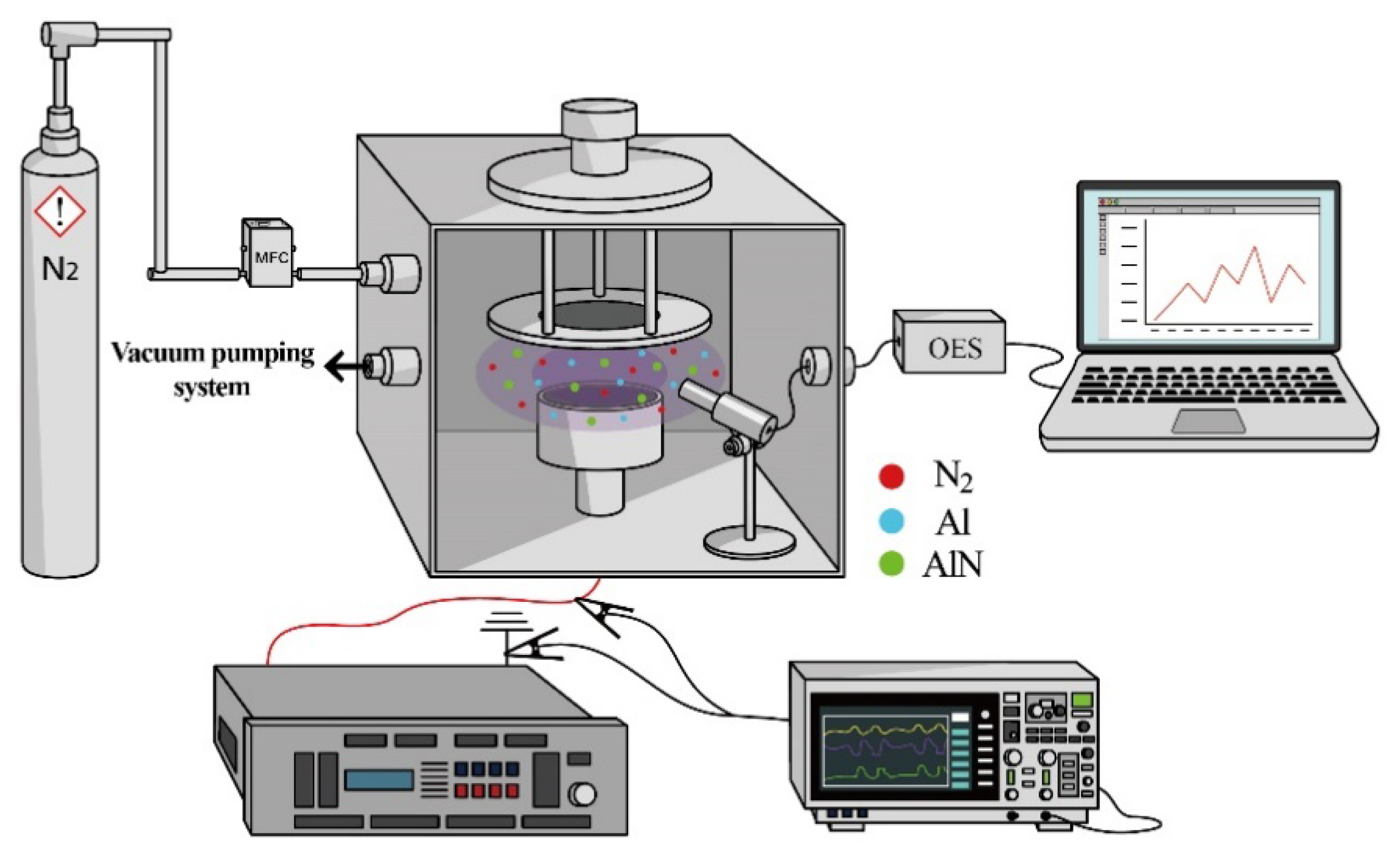
1]. Our previous study has investigated the effect of N2 gas flow and power on the minimum film residual stress of AlN thin films deposited by pulsed DC reactive sputtering on Si (100). Large-scale in-situ OES, XRD, SEM, TEM, FTIR, and alpha-step profiler data were analyzed to determine the film stress states. They proposed a residual stress (VRS) value calculated by a standard deviation in the first principal component direction (PC1-DEV) method. The study suggests a methodology using PCA to determine residual stress characterization as an in-situ plasma monitoring tool for the AlN thin film deposition process [
2].
Plasma properties are studied to better understand plasma vacuum processing and improve process control and repeatability. Typically, duty cycles between 50 and 90 percent and pulse frequencies between 10 and 350 kHz are used throughout the deposition process [
8]. Therefore, understanding the basics of the creation and behavior of pulsed DC magnetron discharges is required to master the new benefits of pulsed DC sputtering. Furthermore, to establish the connections between film properties from film measurements to pulse parameters, it is essential to explain relationships between them and film properties such as film structure, composition, and characteristics, which are particularly interesting for practical applications.
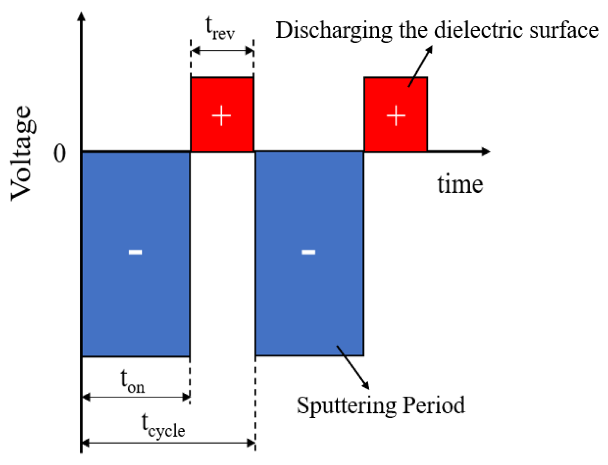
Pulsed DC magnetron sputtering is a widely-used technology in the industry today, and it is especially effective for fabricating materials with excellent electrical insulation properties. It can obtain thin films with high density and good crystallinity at low temperatures [
9,
10,
11,
12]. In the current experiment, AlN films were processed by a reactive DC magnetron sputtering with an asymmetric bipolar-pulsed DC power source at various pulse settings in reverse voltage, pulse frequency, and duty cycle. The asymmetrical bipolar-pulsed DC power supply can adjust its pulse parameters according to requirements to improve efficiency. Compared with radiofrequency (RF) power supply, it can have a better deposition rate and prevents an electrically insulating layer from being deposited on the cathode surface by adding a reverse voltage, which can reduce charge buildup and arcing in affecting film quality [
13]. A typical waveform and pulse feature was shown in
Figure 1. This study used XRD, AFM, and FE-SEM to determine the microstructure of films. RSM, in conjunction with a mathematical Box–Behnken method [
6,
14], was employed to setup a DOE model for how the power supply DC pulse factors impact the microstructural properties of films.
In addition, this study trained thin film quality prediction models through PCA dimensionality reduction combined with the CatBoost model. The CatBoost classifier algorithm was adopted for training transmission line faults data in the multi-dataset from an electrical power system owing to its training speed, accuracy, and ability. The trained model implements an excellent accuracy of 99.54% [
15]. The OES data have been widely built-in virtual metrology (VM) system. Multi-features in OES data are reduced dimensionality using principal component analysis (PCA) [
16]. There is research that presents a non-invasive method for ensuring plasma parameters inside a radio-frequency ion thruster (RIT) by OES data incorporating PCA [
17]. Data preprocessing with a machine learning or deep learning model is already common in artificial intelligence architecture. The PCA preprocessed the OES data, and the results were handed over to the multilayer perceptron (MLP) model for training [
18]. The initialization of the variational autoencoder (VAE) used in MLP had the best result to predict plasma density of etch tool by OES data [
19]. A real-time machine VM based on artificial intelligence has been developed. It can use OES data to supervise plasma nitridation processes in predicting the accuracy of electron temperature at 90% and electron density at 97% [
20]. Another study presented generative adversarial networks (GANs) of deep learning to solve fault detection with imbalanced data in the plasma etching process. It verified the benefits of GANs solving imbalance OES data problems [
21]. This study aims to identify the optimal pulse parameters for producing high-quality AlN films. Additionally, a predictive CatBoost model from PCA was successfully trained by collecting OES data for obtaining film FWHM and grain size.
3. Results and Discussion
AlN films were fabricated using a reactive DC magnetron sputtering with a total of 15 different DOEs combined with three DC pulse parameters in reverse voltage (50–90 V), pulse frequency (100–250 kHz), and duty cycle (80–90%). Pulse parameters have a direct effect on the state of the plasma. Therefore, we optimized the power parameters to obtain better quality of AlN films.
Table 2 presents the 15-run experimental designs from Box–Behnken method.
3.1. Characterization
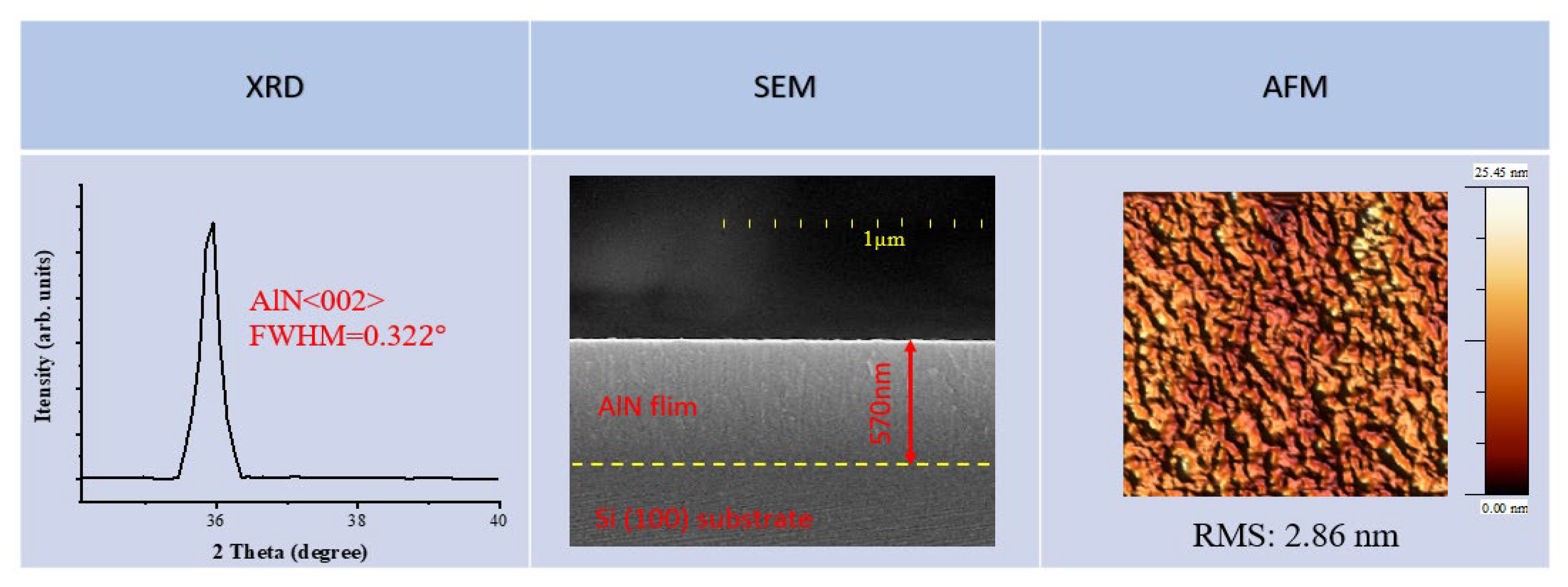
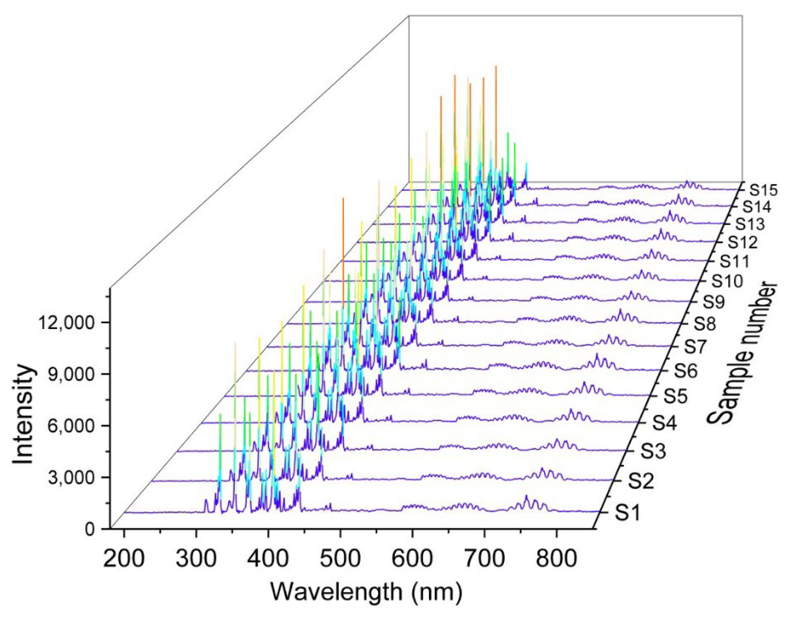
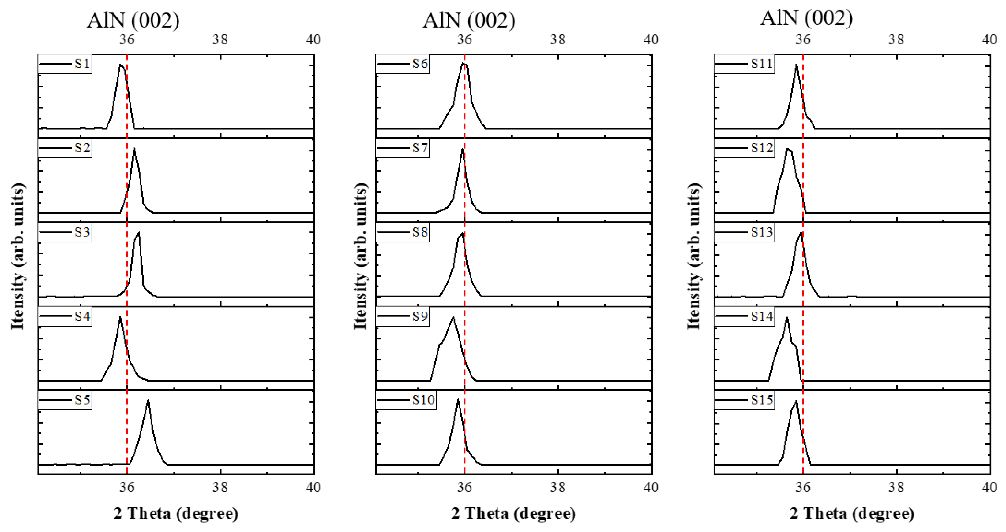
Figure 5 shows XRD (θ/2θ scan) spectra of AlN films (S1–S15) deposited at various sputtering pulse parameters. We observed prominent peaks corresponding to the AlN crystallite phases, which are critical in assessing the quality and crystallinity of the films. These peaks include the (100) and (002) planes, commonly reported in the literature for hexagonal wurtzite AlN films. It can provide insights into the film’s overall purity and the effectiveness of the sputtering process. The microstructures of AlN films were analyzed extensively by XRD scanning in the range of 34°–40°. The impact of three DC pulsed parameters on film FWHM was studied by varying the design of pulse parameters. It can be clearly observed that each group has an obvious AlN 002 peak at about 36°. The film FWHM was obtained by calculations from a Lorentz curve fit in the experimental data between 34° and 38°. Among them, FWHM in fifteen sets of experiments is between 0.1°–0.506°. We observed that experiment S3 has the minimum FWHM value, indicating that the AlN film has better crystallinity under this parameter. In an asymmetric bipolar pulsed-DC reactive sputtering, the reverse voltage is critical. It has to maintain an appropriate value without back sputtering and to prevent the target from poisoning due to the arc causing fine dust particles deposition. The asymmetric bipolar pulsed DC is also dependent on pulse frequency. To prevent the build-up potential (voltage) from crossing the parasitic capacitors, the pulse frequency has to maintain enough beyond its breakdown voltage [
26,
27,
28].
AlN is an excellent piezoelectric material for electroacoustic devices for example, bulk acoustic wave (BAW) and surface acoustic wave (SAW) devices. However, uneven surfaces or microstructure, such as cracks and voids, will cause transmission loss. Furthermore, if the roughness of the surface is greater than the traveling wavelength, the acoustic waves cannot pass through the material surface, which will affect the SAW speed [
5,
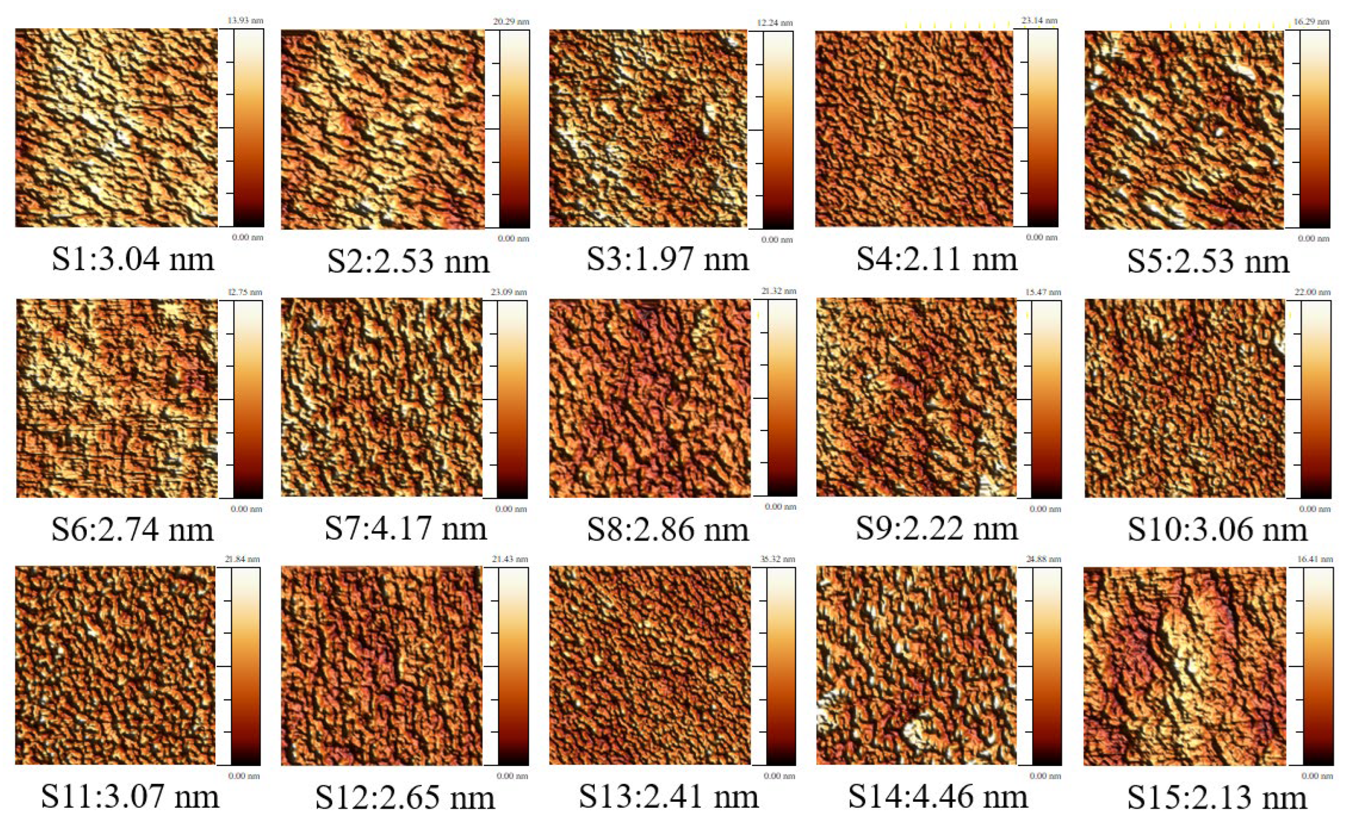
29]. Therefore, the surface roughness is extremely important to the device performance; we use AFM (tapping mode) and FE-SEM to measure the surface roughness, the microscopic crystal morphology, and the cross-sectional structure of AlN films. The results are shown in
Table 3. The surface roughness data are recorded in the center of the film using the tapping mode and the measurement range is 5 µm × 1.2 µm. This mode will bring the probe closer to the sample and increase the amplitude. The amplitude change is used to obtain high-resolution images when contacting the sample. The advantage is that the contact force between the probe and the sample can be reduced, thereby preventing the film surface from scratching. AFM images of AlN films were shown in
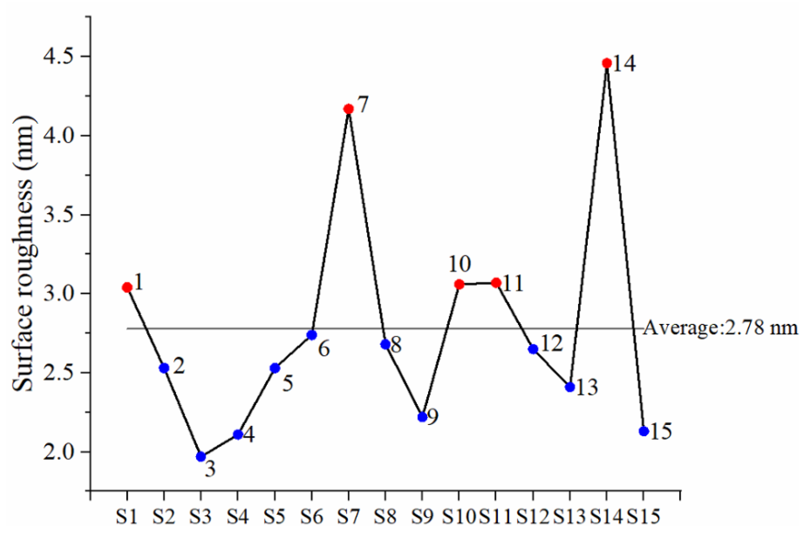
Figure 6. The RMS surface roughness values on 15 sets of AlN films were 1.97 nm–4.46 nm. According to
Figure 7, experiments S1, S7, S10, S11, and S14, which display roughness above the average, all have a reverse voltage greater than or equal to 70 V in common.
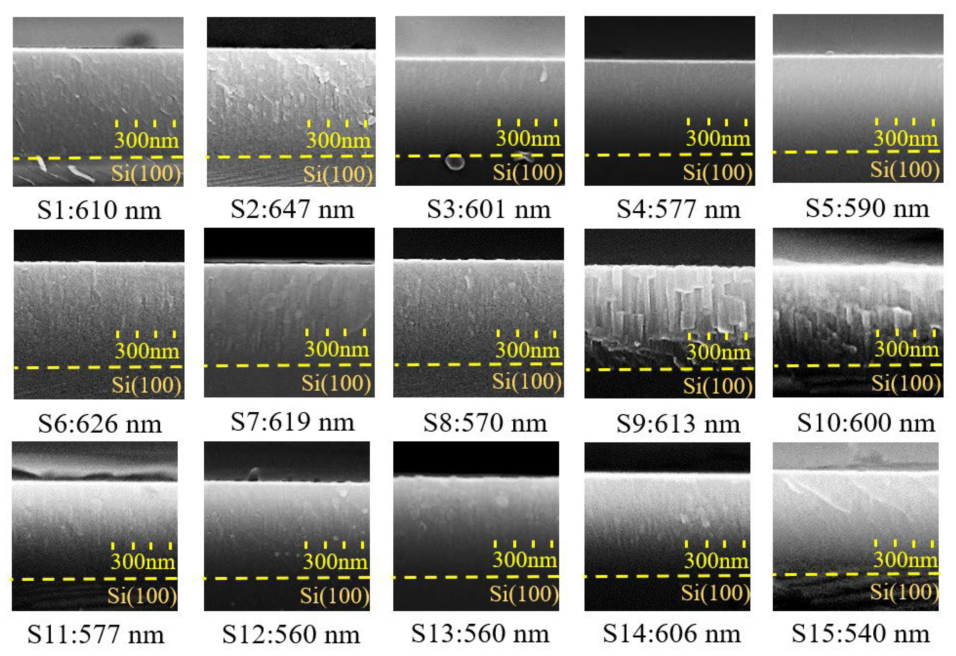
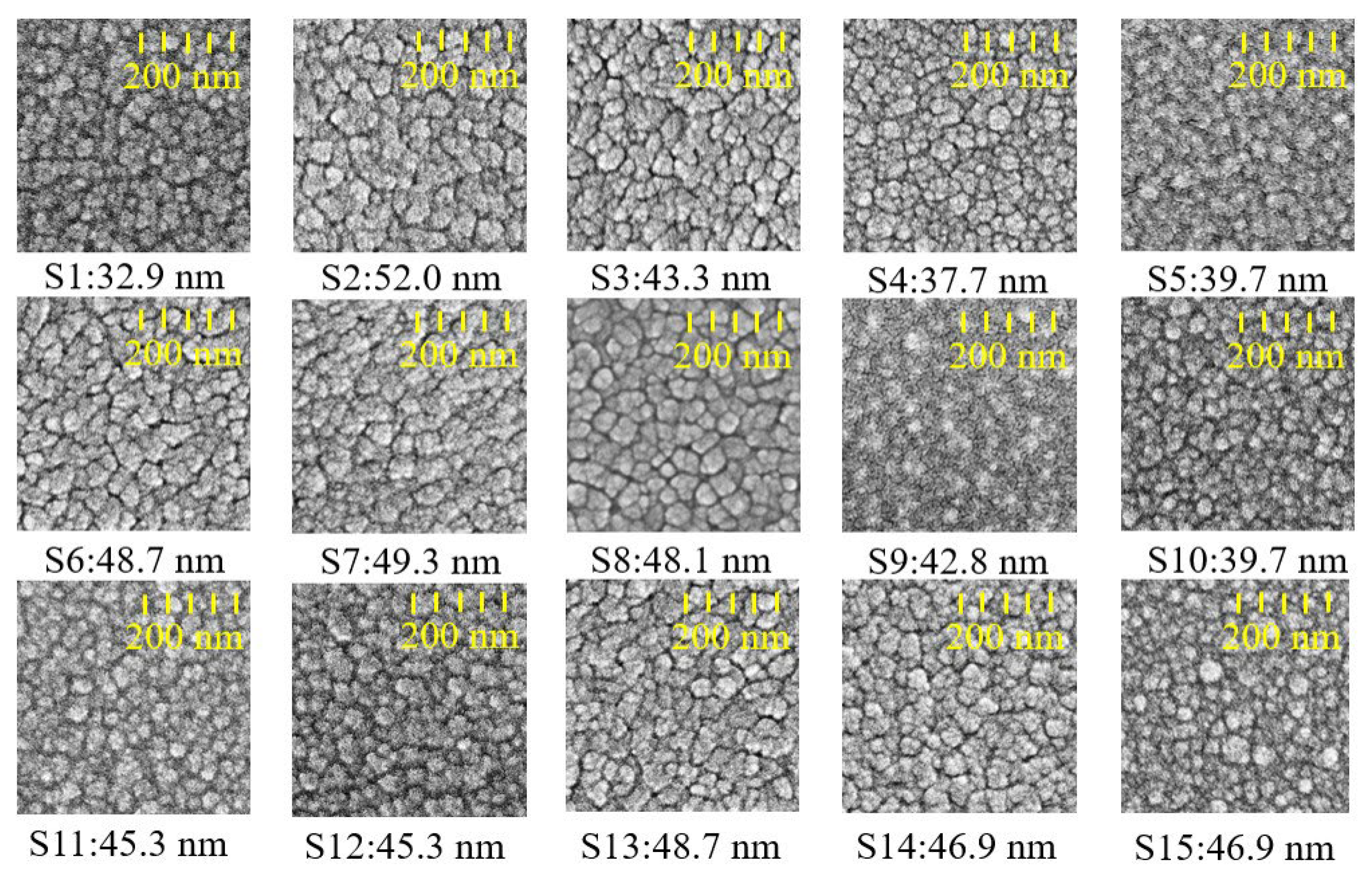
Figure 8 shows the cross-sectional micrographs of AlN films deposited on silicon (100) substrates taken by FE-SEM. The 30 min process exhibited a film thickness between 540–647 nm and a deposition rate of 18.0–21.6 nm/min. It was observed that when the duty cycle was set at a small value (S11, S12, and S15), resulting in a shorter sputtering period (ton), the deposition rate was significantly lower. The duty cycle is proportional to the sputtering period in a complete current waveform. The value represented by the duty cycle is presented in Equation (3). In addition, the increase in pulse frequency will also increase plasma activity. The top-views of AlN films are depicted in
Figure 9. Thin film morphology confirms the XRD data discussed above; the (002) oriented films showed pebble-like structures with average grain sizes ranging between 30.9–52.0 nm, indicating lower surface mobility of adatoms under pure nitrogen conditions [
30] and a clear columnar structure is also shown in the cross-sectional micrographs in
Figure 8.
3.2. Statistical Analysis and Optimization
In this experiment, the Box–Behnken factorial outline with three factors was selected to analyze the three pulse parameters. A linear response equation was generated from the measured and calculated FWHM values. Multiple regression analyses were performed on the experimental data and response variables. We established a second-order polynomial equation, as shown in Equation (4), to explain the relationship between pulse parameters and film FWHM. Equation (4) can predict the response of each factor at three levels (−1, 0, +1), the high levels were labeled as +1, and the low levels were labeled as −1. The reverse voltage (
X1) and duty cycle (
X3) have a more significant linear impact. The coefficients are 0.1064 and −0.238, respectively. In the interaction between pulse parameters, the reverse voltage and duty cycle also have the most significant impact, and its value is −0.001302. According to the above results, the duty cycle (
X3) has the greatest influence, followed by reverse voltage (
X1) and pulse frequency (
X2).
All responses from the results of variance (ANOVA) analysis by a quadratic polynomial model with a corresponding valid model obtained from Minitab 19 software are depicted in
Table 4. In statistical hypothesis testing, the significance level is typically set at 0.05 or below, meaning that results with a
p-value greater than 0.05 are generally not considered statistically significant. In general, the smaller the
p-value is, the more significant the results are, with a
p-value of less than 0.05 indicating strong evidence against the null hypothesis [
31,
32]. It can be seen from the variance analysis of the regression model that the quadratic model has a certain significance, the
p-value is 0.04, and the R-squared value is 85.91%, suggesting that this model has strong explanatory power. Only 14.09% of the total variation remains unexplained, indicating it is a good fit model between the prediction and the data. In addition, the smaller
p-value of the squared and interaction terms of the independent variables indicates a more significant impact of these terms in the model. However, even the R-square (adj) value is 67.13%, and a lower value may suggest a simpler model with fewer variables. The model can still provide valuable insights and predictive power for the response variable.
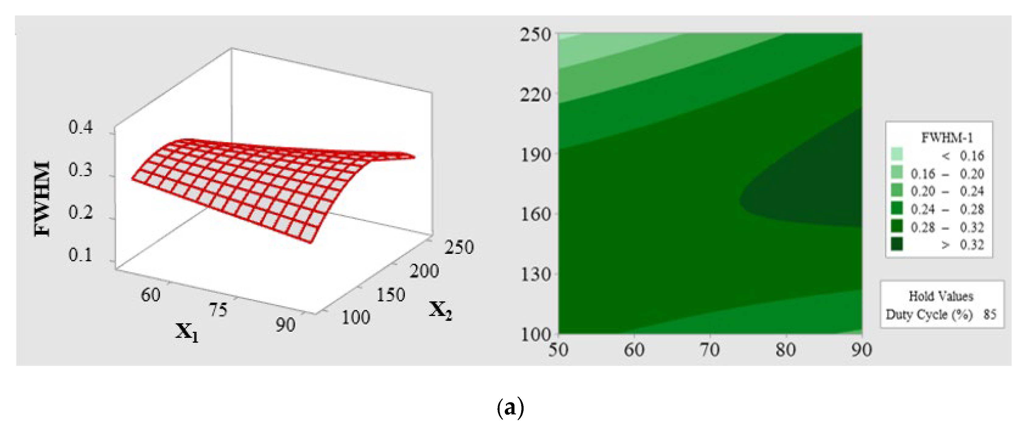
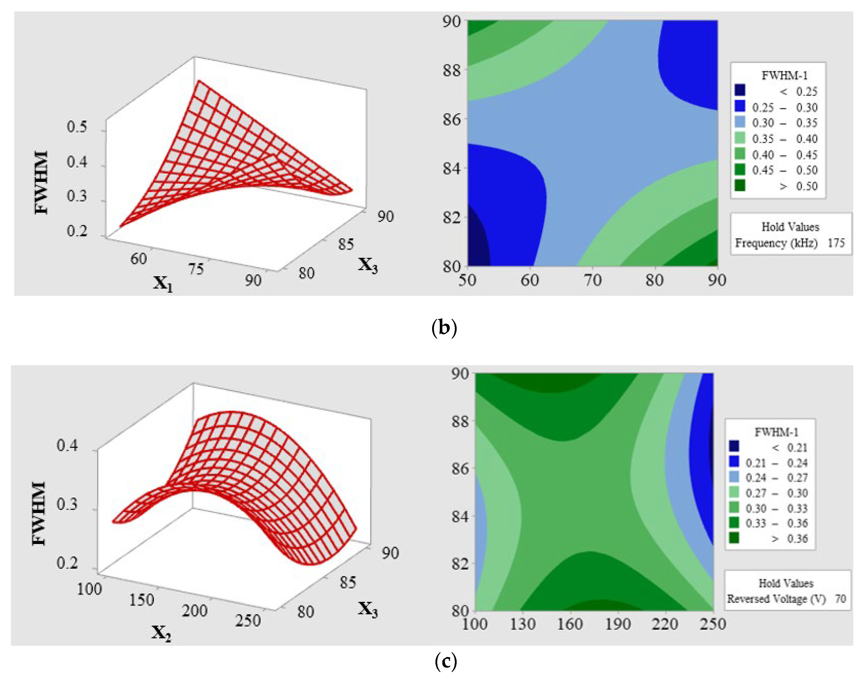
Furthermore, to better visualize and evaluate the effects of pulse parameters on optimizing the FWHM, we converted the above-mentioned second-order polynomial equation (Equation (4)) into 2D and 3D response surface plots. These plots provide an intuitive representation of the relationships among the three main variables (reverse voltage, pulse frequency, and duty cycle), shown in
Figure 10.
In constructing these plots, one parameter was fixed at a medium level, while the FWHM was analyzed as a function of the other two interaction factors. Specifically,
Figure 10a illustrates the response of FWHM when the reverse voltage interacts with the pulse frequency, with the duty cycle held constant at a medium level (85%). The plot shows that better FWHM values are achieved when the reverse voltage is at a low level, and the pulse frequency is at a high level. Similarly,
Figure 10b displays the response of the reverse voltage interacting with the duty cycle while the pulse frequency is maintained at a medium level (175 kHz). Lastly,
Figure 10c presents the response of the pulse frequency interacting with the duty cycle, with the reverse voltage fixed at a medium level (70 V).
By examining these response surface plots, we can gain a deeper understanding of the complex interactions among the pulse parameters, which aids in optimizing the FWHM based on the second-order polynomial equation (Equation (4)).
In summary, the response of the interaction of multiple variables in the above RSM diagram is integrated, and a set of optimized parameters is obtained, presented in
Table 5. The best results obtained in this research are reverse voltage 50 V, pulse frequency 250 kHz, and duty cycle 80.6061%. The estimated FWHM value is 0.11°. Due to the much higher mobility of electrons compared to ions, the positive voltage is usually set at 10–20% of the negative working voltage to achieve complete discharge. However, it must be kept low enough to prevent the occurrence of back sputtering and reduce the risk of arc and target poisoning. Deposition at higher pulse frequencies enhances plasma activity and concentration, resulting in better film uniformity. Additionally, a higher duty cycle could result in an increase in the sputtering period, which may lead to a better deposition rate. However, it could also cause a breakdown voltage exceeding the parasitic capacitors on target, resulting in arcing and subsequently deteriorating the quality of the deposited film [
28,
33].
3.3. Data Preprocessing and Model Training
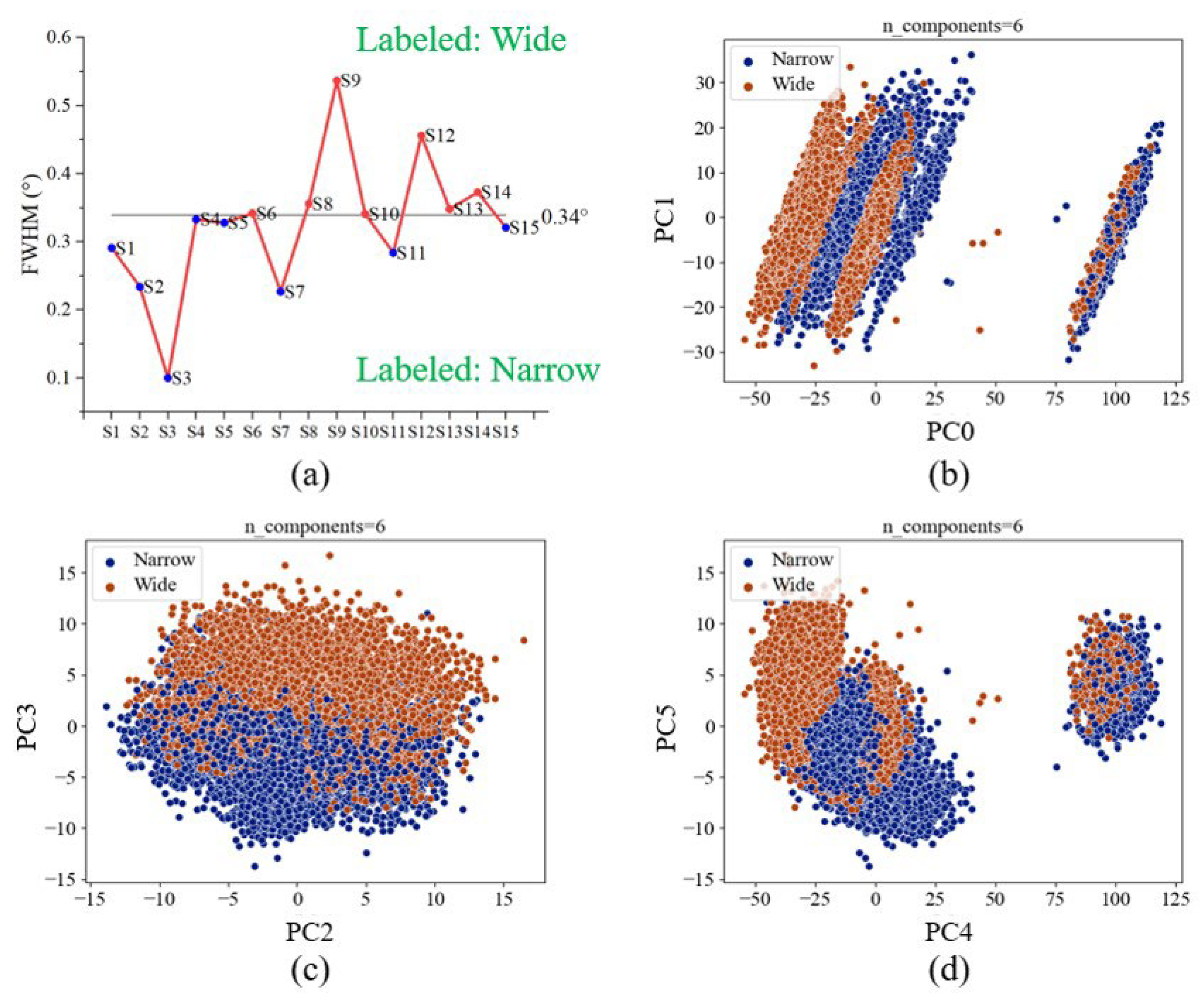
We trained two CatBoost models to classify FWHM and grain, respectively. For the FWHM model, if the measured data exceeds the average value of 0.34 degrees, we label it as “Wide”, and the opposite is labeled as “Narrow”. The schematics of the labeled data are shown in
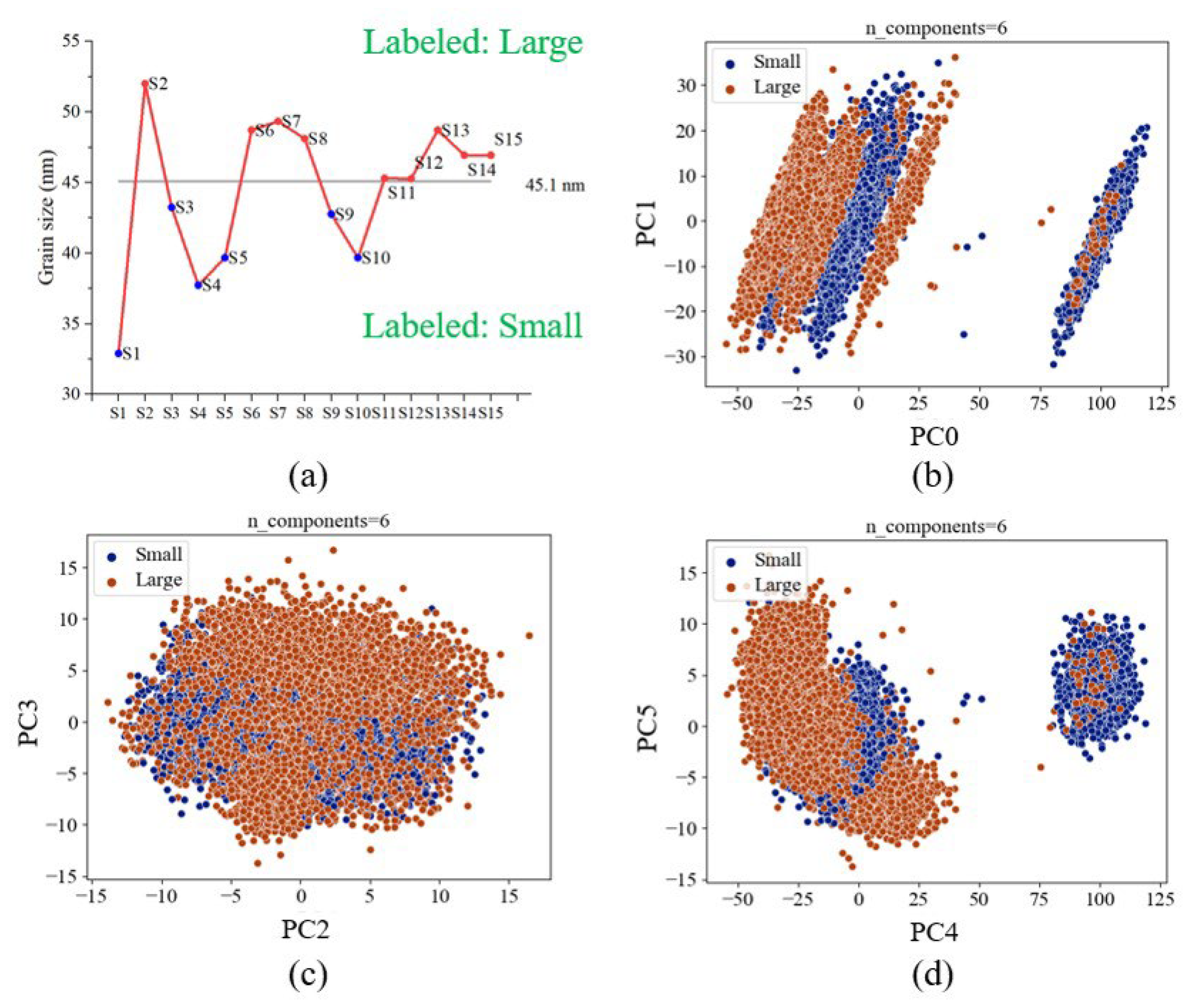
Figure 11a. For the grain size model, if the measured data exceed the average value of 45.1 nm, we label it as “Large”, and the opposite is labeled as “Small”. The schematic of the labeled data is shown in
Figure 12a.
For data preprocessing, we use PCA to reduce the dimensionality of OES data from 1900 features to 6 features (PC0 to PC5). After PCA dimensionality reduction, the data is transformed into a new set of principal components (PCs) that capture the maximum variance in the original dataset. The cumulative variance is the sum of variances of the principal components (eigenvalue of the covariance matrix illustrated in
Section 2.4). The means of the cumulative variances increase as the number of principal components increases. Typically, we hope to select the smallest number of principal components that capture a large percentage of the total variance, to reduce the dimensionality of the data and simultaneously preserve the information as much as possible. The cumulative variances from PC0 to PC5 are 73.59%, 79.12%, 82.51%, 84.73%, 89.12%, and 91.14%, respectively. The cumulative variances mean the total variation in a dataset explained by each principal component. From the calculation results using Python software (scikit-learn toolkit), we can interpret 91.14% of the features in the dataset through six principal components. The dimensionality data can improve the calculating time and eliminate outliers and visualization effectively after dimensionality reduction. From the visualized results, the same labeled data are well clustered. The well-clustered data refer to a dataset where the data points are grouped closely together after transformed space. When the data is well-clustered, it becomes easier for machine learning models to learn the relationships between the features and the target variable. As a result, machine learning models trained on well-clustered data tend to have better training performance, including higher accuracy and faster convergence during training.
Figure 11b,c and
Figure 12b,c, show the results of dimensionality reduction. The blue and orange dots signify two distinct types of data. Despite the proximity of the clusters, the results of the dimensionality reduction reveal a clear and discernible clustering pattern. This noticeable separation between the data groups suggests that the accuracy of the prediction model is likely to be enhanced. Consequently, the clustering visualized in the figure serves as a valuable indicator of the model’s potential performance.
The machine learning model training process typically involves two important steps: data split and hyperparameter tuning. The data split involves dividing the available dataset into training, validation, and testing sets. The training data are used to train the model, while validation data are used to evaluate the model’s performance during training and select the best hyperparameters. Finally, the test data are used to evaluate the final performance of the trained model after hyperparameter tuning. Hyperparameter tuning involves selecting the best value of hyperparameters that maximizes the model’s performance on validation data. Once the best set of hyperparameters is selected, the model can be trained again using the entire training data, and the final performance can be evaluated on the test data. Following these two steps can ensure that the machine learning model is properly trained and optimized for the given dataset.
For CatBoost model training, the datasets have been split into the training dataset 70%, the validation dataset 15%, and the testing dataset 15%. This distribution to splitting dataset into training, validation, and test subsets allows for a sufficiently large training set (70%) to develop and refine the prediction model while also providing separate validation (15%) and test (15%) sets to assess its performance and generalization capabilities. The validation set is useful for tuning model parameters and preventing overfitting, while the test set serves as a final evaluation to ensure that the model performs well on new or unseen data. This method of dataset partitioning is commonly used in machine learning applications and is considered good practice for robust model evaluation. We mainly tuned the parameters of iteration and learning rate. We fixed the parameters of max_depth = 3 and l2_leaf_reg = 4, and both the FWHM and grain size models are set to be the same iteration (=1000) and learning rate (=0.01). The max_depth and l2_leaf_reg are the hyperparameters in the CatBoost. The parameters of the max_depth can control the maximum depth of each decision tree in the ensemble model (CatBoost in this study). The l2_leaf_reg can control the L2 regularization to the leaf weights of each decision tree in the ensemble. The best value for max_depth and l2_leaf_reg depends on the scale and complexity of the dataset. Then the trained model for FWHM and grain size received the performance metrics as shown in
Table 6. The FWHM model had a recall of 89.52%, precision of 94.51%, F1-score of 91.95%, and accuracy of 90.67%. The grain size model had a recall of 86.40%, precision of 79.61%, F1-score of 82.87%, and accuracy of 82.07%. Four basic terms that refer to four possible outcomes of binary classification in machine learning are the values of
TP (true positive),
TN (true negative),
FP (false positive), and
FN (false negative). TP and TN are correct prediction results, and
FP and
FN are incorrect. The values of
TP,
FP,
FN, and
TN as accuracy, precision, recall, and F1-score, respectively, can be adopted to evaluate the performance of a prediction model. Details are illustrated in Equations (5)–(7).
4. Conclusions
We use Box–Behnken experimental design to reduce the number of experiments and collected data to develop a reliable model, which enables us to make more appropriate adjustments to parameters according to device requirements, thus saving a lot of time and effort in improving its quality. We obtained the optimized conditions of the pulse parameters of the best FWHM as reverse voltage: 50 V, pulse frequency: 250 kHz, and duty cycle: 80.6061%. In addition, using AFM and SEM to analyze the film’s microstructure, the relationship among surface roughness, deposition rate and pulse parameters was obtained. We compared relevant literature and found that the FWHM ranged from 0.28°–0.36° and decreased with a decrease in duty cycle (20–70%). However, the pulse frequency used in the literature was 100 kHz, which may not be sufficient to achieve the desired plasma activity and concentration [
34]. Compared with other studies using asymmetric bipolar pulse deposition of AlN thin films, our results also showed better performance [
35]. This study also successfully trained two models that can predict film FWHM and grain size. Machine learning algorithms can analyze amounts of data and identify OES data features that are difficult for humans to find. Accurately predicting a semiconductor deposition process can reduce the number of failed runs and improve overall efficiency. It can make more accurate predictions about the deposition process, reducing the time and cost required for testing. Moreover, machine learning algorithms can provide insights into the deposition process that may not be apparent through traditional analysis methods. This can help engineers make more informed decisions about the process and improve the overall quality of the semiconductor products produced. In the future, we will develop more expertise in plasma physics, data analysis, and machine learning, as well as access to the necessary equipment, and data (parameters) to develop a complete plasma information-based virtual metrology (PI-VM) system. This can provide real-time feedback to engineers, enabling them to optimize the semiconductor processing and improve yields. We know that uncertainty factors can impact the prediction model, specifically the blank signals and noise measured by the OES during the setup period. Suppose these noise components are inadvertently included in the model training process without proper attention or filtering. In that case, the model’s prediction accuracy may be compromised, resulting in errors and reduced reliability of the predictions. The novelty of this study is that it verifies the application of the PCA method to rapidly reduce the dimensionality of OES data and validates the feasibility of using reduced OES data for predicting film quality (FWHM and grain size). Since the prediction model belongs to a classification model that classifies two classes (above or below the average value), it cannot be used to predict the actual value of FWHM and grain size. A predictive model of actual values is planned for the future.
5. Future Work
One of the primary goals for our future studies is to investigate the density of AlN films, as it is a crucial parameter for semiconductor applications and is directly related to the sputtering parameters. We will explore opportunities for collaboration with other laboratories or institutions to access this technology. By utilizing X-ray reflectivity (XRR) equipment, and measurements, we can estimate the density of the AlN films and examine its relationship with the sputtering conditions. Furthermore, we will seek to refine our prediction model by incorporating additional parameters, such as film stress, adhesion, and thermal conductivity, to achieve a more comprehensive understanding of the film properties. Additionally, we plan to compare the results obtained using our optimized parameters with previously published studies to validate the effectiveness of our approach. Through these efforts, we aim to enhance the optimization of sputtering parameters for AlN film deposition in semiconductor applications and contribute to the broader body of knowledge in this field.
In the upcoming experiments, we will model and simulate the problem of target erosion. First, develop a computer model to simulate the sputtering process and predict the effect of target erosion on film properties. The model incorporates parameters such as target material, deposition conditions, and erosion rate Incorporate parameters such as target material, deposition conditions, and erosion rate. Then, use the model to simulate the sputtering process under varying degrees of target erosion and predict the corresponding film properties. The software expected to be used for computer modeling and simulation of sputtering processes is COMSOL Multiphysics.

 ,
, 


