
Polycrystalline WO3−x Thin Films Obtained by Reactive DC Sputtering at Room Temperature

Centro de Investigaciones Energéticas Medioambientales y Tecnológicas (CIEMAT), Avda. Complutense 40, 28040 Madrid, Spain
Materials 2023, 16(4), 1359; https://doi.org/10.3390/ma16041359
Submission received: 16 January 2023
/
Revised: 2 February 2023
/
Accepted: 3 February 2023
/
Published: 6 February 2023
(This article belongs to the Special Issue Sputter Deposition/Physical Vapor Deposition (PVD) Materials and Processes)
Abstract
:Tungsten oxide thin films have applications in various energy-related devices owing to their versatile semiconductor properties, which depend on the oxygen content and crystalline state. The concentration of electrons increases with intrinsic defects such as oxygen vacancies, which create new absorption bands that give rise to colored films. Disorders in the crystal structure produce additional changes in the electrical and optical characteristics. Here, WO3−x thin films are prepared on unheated glass substrates by reactive DC sputtering from a pure metal target, using the discharge power and the oxygen-to-argon pressure ratio as control parameters. A transition from amorphous to polycrystalline state is obtained by increasing the sputtering power and adjusting the oxygen content. The surface roughness is higher and the bandgap energy is lower for polycrystalline layers than for amorphous ones. Moreover, the electrical conductivity and sub-bandgap absorption increase as the oxygen content decreases.
1. Introduction
Tungsten oxides are naturally abundant, environmentally friendly, and their semiconductor properties can be tuned according to oxygen content and crystalline state [1]. Furthermore, they are easily produced in the form of thin films or coatings, making them special candidates for a variety of energy-related applications, such as smart windows [1], batteries [2], photocatalysis [3] or solar cells [4], and also for faster gas sensors [5].
WO3 bulk crystals are built up from [WO6]6− octahedra, where the tungsten atom is placed in the center of the octahedra with the oxidation state W6+. The ideal WO3 crystal consists of ordered networks of corner-sharing octahedra, but in practice, different phases can be obtained due to atomic displacements and rotations, which reduce the crystal symmetry. Monoclinic WO3 is the most stable phase at room temperature (17 °C < T < 330 °C), converting to orthorhombic and tetragonal symmetries at 330 °C and 740 °C, respectively [1]. These crystalline phases can be described as distortions of the cubic ReO3-type structure, explained by the low formation energy for defects in the cubic lattice [6]. If WO3 is reduced, oxygen loss induces new structural features, giving rise to non-stoichiometric phases WO3−x (0 < x < 0.4) where blocks of corner-sharing octahedra are connected by edge sharing [2].
Perfect WO3 is a transparent insulating semiconductor with a bandgap energy of 2.7 eV [3], but in reality the electrical and optical characteristics of tungsten oxides are highly dependent on their crystalline structure and oxygen content. The electron concentration can be increased by intrinsic defects such as oxygen vacancies (VO2+), which create new absorption bands below the conduction band and, as a result, color appears from bluish to dark gray [7]. For technological applications, thin films of WO3−x are particularly attractive, considering that additional changes in electrical and optical characteristics can be achieved by reducing the crystal size into the nanometer range [8].
Sputtering has been widely used to prepare tungsten oxide thin films with controllable microstructures and tunable physical properties. Moreover, reactive DC sputtering via a metallic W target provides the advantages of low cost and high deposition rates [9]. It is known that amorphous tungsten oxide coatings are commonly achieved by DC sputtering on unheated substrates [10,11,12]. Subsequent heating in the 400–500 °C range is needed to achieve crystallization in the monoclinic WO3 [10] or monoclinic W18O49 [11] structures. Otherwise, a stable orthorhombic WO3 phase has also been obtained from amorphous layers grown under a low oxygen content atmosphere, by subsequent annealing in air at 400–600 °C [12]. Only small WO3 crystallinity has been reported for low substrate temperatures (≤200 °C), highly dependent on the sputtering power [13], the working pressure [14] and the oxygen partial pressure [15].
In this work, polycrystalline WO3−x thin films consisting of WO3 together with W3O8 or W18O49 crystalline phases are obtained directly on unheated glass substrates by reactive DC sputtering from a pure metal target. A transition from the amorphous state to orthorhombic or monoclinic symmetries is achieved by increasing the sputtering power and the oxygen-to-argon pressure ratio. The structure, morphology and optical and electrical characteristics of the samples are analyzed as a function of the preparation conditions to determine the different effects of crystallinity and oxygen vacancy defects.
2. Materials and Methods
Tungsten oxide layers were prepared on unheated soda-lime glass substrates by reactive DC magnetron sputtering from a W target (purity 99.99%) of 15 cm in diameter. The chamber was evacuated to a base pressure of 4 × 10⁻⁴ Pa before introducing a fixed argon flow of 60 sccm and an adjusted oxygen flow in the 3–30 sccm range, using independent mass flow controllers. The oxygen flow was varied to achieve different oxygen partial pressures, Opp (%) = 100 p(O2)/[p(O2) + p(Ar)], in the range 5–30%. Then, a DC source was connected to the target, operating at a constant power value set to 200 or 400 W, resulting in a power density of 1 W/cm2 or 2 W/cm2, respectively. The growth rate was about 25 nm/min at the lowest power density and about 50 nm/min at the highest, with only minor variations at different oxygen pressures in the present range. For each case, the deposition time was adjusted to obtain a same film thickness of 300 ± 20 nm.
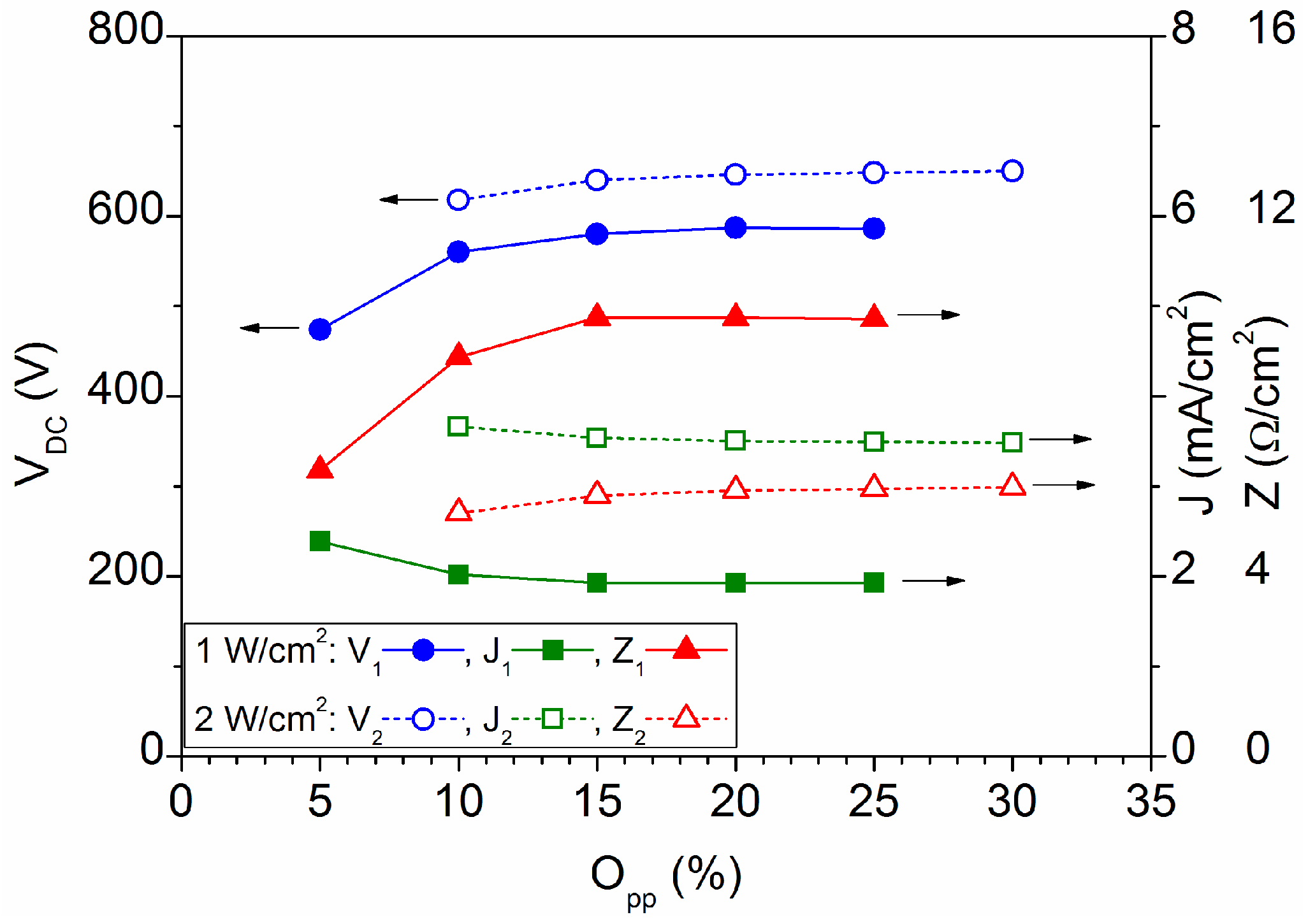
Figure 1 shows the current, voltage and impedance characteristics as a function of oxygen percentage for the two power values applied to the target. The range studied goes from 5% to 30% Opp, which corresponds to oxygen gas inputs from 4 sccm to 30 sccm. Therefore, all processes were carried out in the oxide operating mode of the target. The impedance of the discharge increases with the increase of the oxygen content in the chamber, which is attributed to a greater capture of electrons from the plasma due to the high electronegativity of oxygen [16]. Otherwise, the impedance is always lower when the applied power is higher, which is related to a better sputtering efficiency due to an important increase of the ion current in the plasma at high power [17]. The discharge current is the sum of the ion current (Ii) and the electron current (Ie), being Ii increasing with the sputtering power, while Ie decreases when the oxygen percentage increases.
The crystallographic properties of the samples have been examined by X-ray diffraction (XRD) with radiation Cu K-α1 (λ = 1.54056 Å) in a Philips X’pert instrument, using Bragg–Brentano θ−2θ configuration. The standard powder diffraction files (PDF) were used to identify the crystalline phases in the diffractograms. Elemental compositions were obtained by electron probe micro-analysis in a JEOL JSM-6400 operating at 20 kV. The topography was examined by atomic force microscopy (AFM) with a Park XE-100, which allows surface roughness to be quantified from digital images. The optical characterization uses transmittance (T) and reflectance (R) measurements performed with a Perkin–Elmer Lambda 9 double beam spectrophotometer, in a wavelength range from 250 to 2500 nm and taking the air as reference. The transmittance is corrected for reflection losses, Tc (%) = 100 T(%)/(100 − R(%)), and the optical absorption coefficient is calculated as [18,19]: α = (1/t) ln[100/Tc(%)], including the film thickness value (t) obtained with a Dektak 3030 profilometer. The electrical conductivity of the layers has been determined with a four-point probe system Veeco FPP5000.
3. Results and Discussion
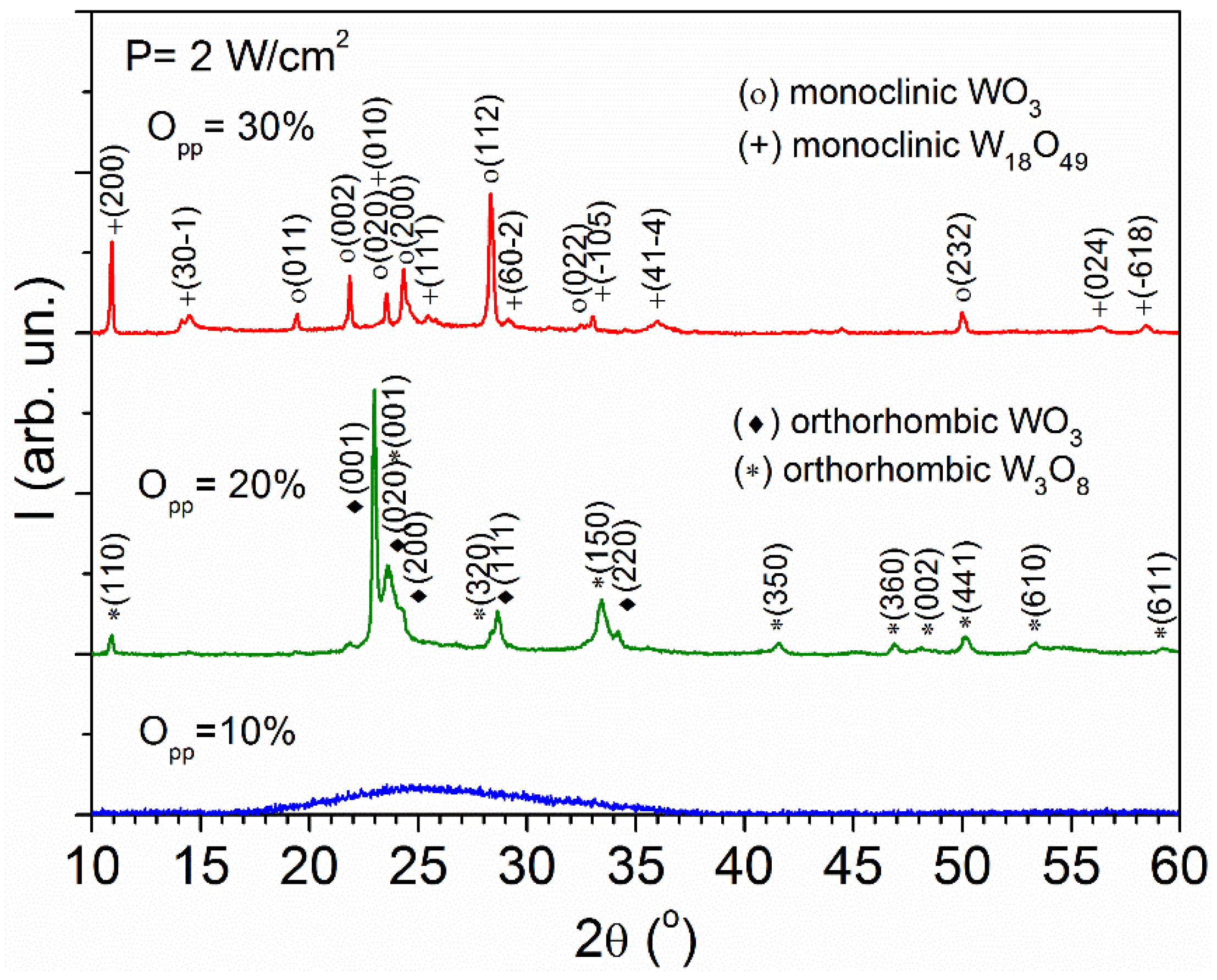
The XRD patterns measured for the various samples have proven that the tungsten oxide films prepared at P = 2 W/cm2 and Opp = 20–30% have a polycrystalline structure, while all other layers are amorphous, as indicated by absence of diffraction peaks in their respective patterns. The data summarized in Table 1 indicate that both the sputtering power and the oxygen pressure influence the composition and crystallinity of the tungsten oxide coatings, in a similar way to that observed in other works [13,15,20]. Films may grow amorphous due to high density of oxygen vacancies [7] or low energy of the particles impinging on the substrate [19].
According to Figure 2, the layer grown at P = 2 W/cm2 and Opp = 20% exhibits XRD peaks that correspond to orthorhombic WO3 (PDF#20-1324) and orthorhombic W3O8 (PDF#65-1175). The strongest peaks are recorded at 2θ = 22.94° and 2θ = 23.54°, assigned to the (001) planes of WO3 and W3O8, respectively. Otherwise, films prepared at P = 2 W/cm2 and Opp = 30% show a mixture of monoclinic WO3 (PDF#83-0950) with a strong (112) peak at 2θ = 28.33°, and monoclinic W18O49 (PDF#36-0101) with strong (200) peak at 2θ = 10.91°. It is known that monoclinic is the most stable WO3 phase at room temperature and symmetries higher than the monoclinic may result from static disorder [6], attributed to the presence of clusters of edge-sharing octahedra randomly distributed in the lattice. Such a tendency is also found in the oxygen-deficient WO3−x phases, but in this case the edge-sharing octahedra are not randomly distributed since they are in periodic patterns. Specifically, the W3O8 structure contains groups of four edge-sharing WO6 octahedra mutually linked by corner-sharing with single octahedra [21]. Otherwise, the W18O49 structure contains both octahedral and pentagonal bipyramidal coordination of the metal atoms by oxygen [22]. Analogous W3O8 and W18O49 phases have been obtained by reduction of tungsten trioxide or by heating appropriate mixtures of W and WO3 [21,22,23].
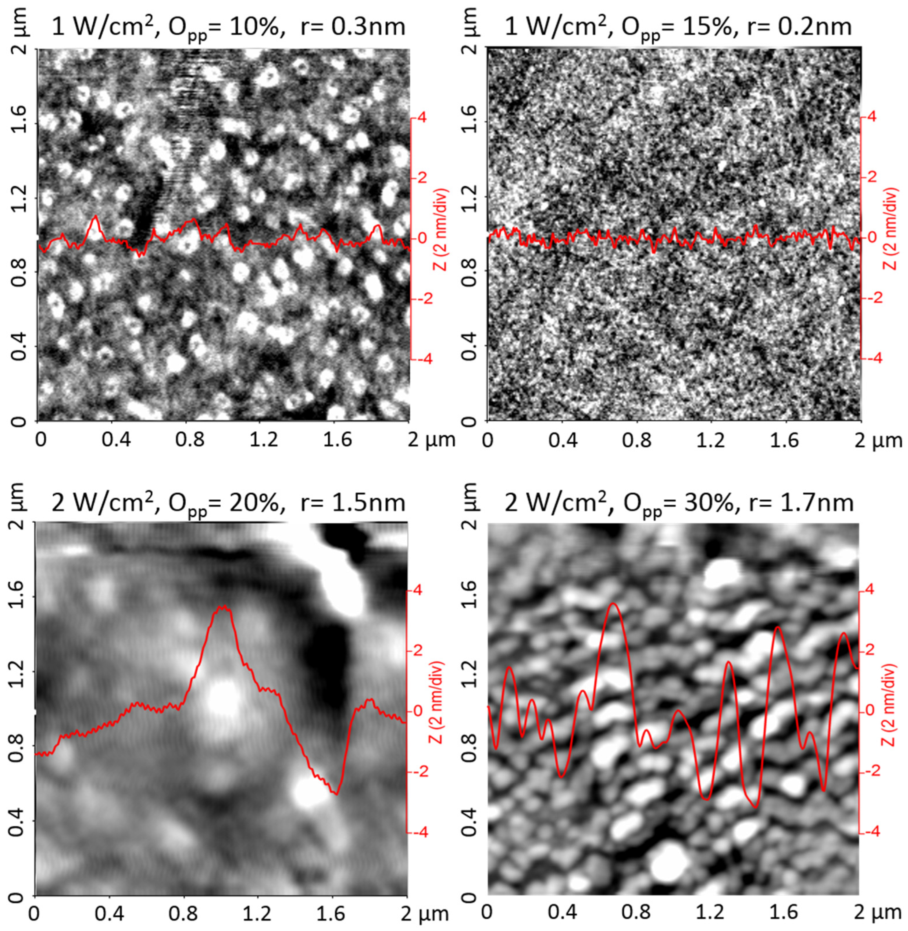
The surface morphology and corresponding root-mean-square roughness value (r) of the samples are illustrated in Figure 3, by representative AFM images on 2 μm × 2 μm areas. A line scan taken in the middle of each image is included for comparison. It can be seen that the amorphous layers grown at P = 1 W/cm2 are constituted by small grains that give smooth surfaces, with r ≤ 0.3 nm. Increasing the sputtering power to P = 2 W/cm2 promotes the growth of larger grains that clump together to form cauliflower-like clusters, with a significant increment of the surface roughness to r ≥ 1.5 nm. This is related to the crystallization of the layers (Figure 2), since by increasing the sputtering power, the deposited particles can obtain enough energy to migrate along the surface and inside, which favors the formation of crystalline structures and larger clusters that increase the surface roughness. A similar increment in the root-mean-square roughness from amorphous to polycrystalline films has been reported for other sputtered WO3 coatings [10,12].
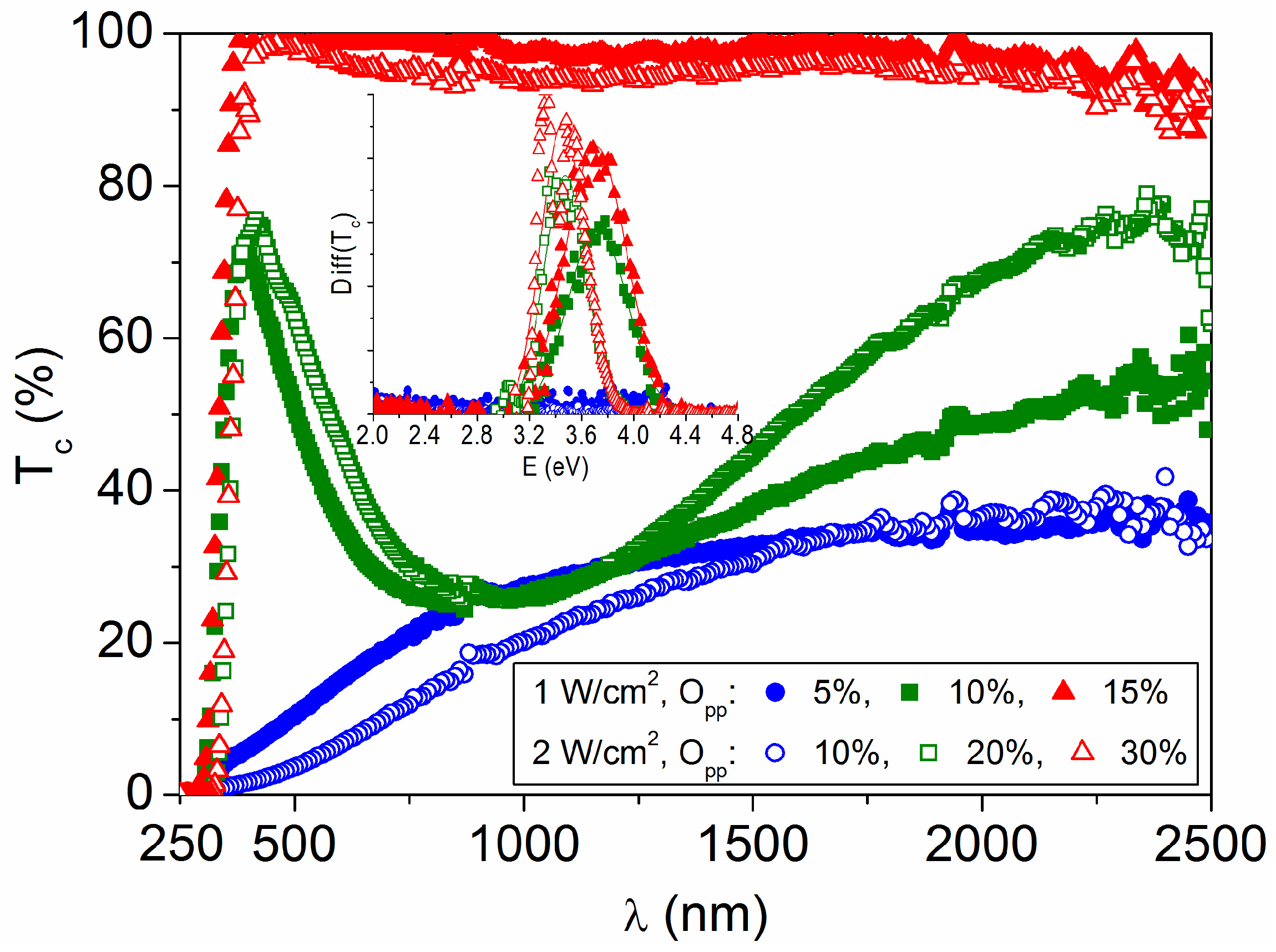
The optical transmittance of the tungsten oxide films is plotted in Figure 4 as a function of the light wavelength. For each sputtering power, the layers prepared at high oxygen pressures are transparent in the visible and near-infrared regions, as expected for stoichiometric WO3 [19], but the transmittance decreases when the oxygen content decreases. The strong transmittance decline in the near infrared (green plots in Figure 4) and also in the visible range (blue plots in Figure 4) indicates the presence of oxygen vacancy defects (VO+ and/or VO2+) together with tungsten atoms in a lower oxidation state (W5+ and/or W4+), which are responsible for sub-bandgap absorption [18,24]. Such intrinsic defects can be tuned by the preparation conditions, taking into account that a higher discharge power can sputter more metal atoms requiring higher oxygen content in the chamber to achieve near-stoichiometric ratios, as it is evidenced by the transmittance spectra and the other data in Table 1.
The bandgap energy (Eg) for each sample is estimated as the inflection point of the respective transmittance curve [25], the peak of the derivative dTc/dE, which is included in the Figure 4 inset. This is a good approximation for the bandgap of extended states, when the edges of the valence and conduction bands are not abrupt, and the tail states complicate the optical transitions [26]. The layers with the lowest oxygen content (O/W ~ 2.60 atomic ratio) have a metallic behavior that prevents bandgap determination. A semiconductor-to-metal transition is expected in WO3−x by increasing the oxygen deficiency, when the Fermi energy falls in a continuum of electronic states due to the increment of intrinsic defects [27]. The coloration (visible absorption) is accompanied by a proportional change in the electrical conductivity of the samples, which is given in Table 1, because the oxygen vacancy defects are acting as electron donors [24]. The metallic films are amorphous regardless of the sputtering power used. Other amorphous layers, prepared at P = 1 W/cm2 and Opp ≥ 10%, show Eg = 3.71 ± 0.1 eV, while polycrystalline coatings prepared at P = 2 W/cm2 and Opp ≥ 20% show a lower Eg = 3.46 ± 0.1 eV. These values are in accordance to those reported by other authors, being generally higher for amorphous WO3−x layers than for polycrystalline ones [10,28], and clearly superior to the bandgap of bulk WO3, which is 2.71 eV [7]. In disordered films, bandgap widening has been attributed to quantum confinement, since the length over which the electrons can move freely is limited [29].
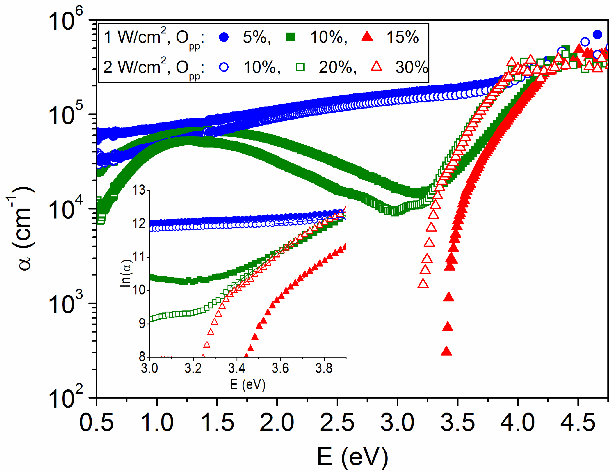
The influence of defects and disorder on the optical characteristics is also evaluated from the absorption spectra plotted in Figure 5 for the various WO3−x films. At light energies just below the bandgap value (E < Eg), the extent of the absorption edge is characterized by the Urbach energy, EU, which indicates the width of the band tails of the localized states within the bandgap region. The calculations in the Figure 5 inset prove that the experimental data follow Urbach’s rule [30]: α = α0 exp(E/EU), with the respective EU values listed in Table 1. The highest Urbach energies (EU > 1.5 eV) correspond to the amorphous films with metallic character, which show a residual absorption (α > 0) throughout the measured spectrum and are brown in color. Otherwise, the Urbach energy is minimal (EU = 0.18 ± 0.01 eV) for the transparent layers close to WO3 stoichiometry, with no significant difference between their amorphous or polycrystalline nature, as observed for other WO3 films [31,32]. In the intermediate conditions, the samples exhibit slightly higher values (EU = 0.21–0.29 eV) and bluish-gray color due to the selective absorption band located around 1.4 eV, which is typical of WO3−x coatings with x = 0.2–0.3 [20]. Therefore, EU values depend mainly on the oxygen vacancy states, as has been found in previous works [30,31].
4. Conclusions
The composition, structure and physical properties of reactively sputtered WO3−x films can be tuned by discharge power and oxygen partial pressure. The films grow amorphous when the energy of the particles impinging on the substrate is not high enough or when there are high oxygen vacancy densities due to low oxygen content (O/W ≤ 2.6). Increasing the sputtering power and the oxygen pressure makes it possible to obtain a mixture of orthorhombic WO3 and W3O8 with an overall composition O/W = 2.82 or a mixture of monoclinic WO3 and W18O49 with O/W = 2.98.
Surface roughness is higher for polycrystalline coatings (r > 1.5 nm) than for amorphous ones (r < 0.3 nm), because of the formation of large grains that clump together to form cauliflower-like clusters when the energy of the deposited particles increases. Otherwise, the bandgap energy is higher for amorphous films (Eg = 3.71 ± 0.1 eV) than for polycrystalline ones (Eg = 3.46 ± 0.1 eV), which is attributed to gap widening by quantum confinement in disordered samples.
All layers prepared at high oxygen pressures have low conductivity (σ~10−4 S/cm) and high transparency in the visible and near-infrared regions. Some coloration appears when the oxygen content decreases, due to sub-bandgap absorption by oxygen vacancy defects, which also increase the electrical conductivity. The samples with the lowest oxygen content (O/W ≤ 2.6) have a metallic behavior, with high conductivity (σ~101 S/cm) and high Urbach energy (EU > 1.5 eV), resulting from a large number of localized states within the bandgap region. For the other films, the Urbach energy is in a lower range EU = 0.18–0.29 eV, being more dependent on the oxygen vacancy states than on the crystalline order.
Funding
This research received no external funding.
Institutional Review Board Statement
Not applicable.
Informed Consent Statement
Not applicable.
Data Availability Statement
The data are available in this article.
Conflicts of Interest
The author declares no conflict of interest.
References
- Zhang, M.; Yang, C.; Zhang, Z.; Tian, W.; Hui, B.; Zhang, J.; Zhang, K. Tungsten oxide polymorphs and their multifunctional applications. Adv. Colloid Interface Sci. 2022, 300, 102596. [Google Scholar] [CrossRef]
- Shinde, P.A.; Jun, S.C. Review on recent progress in the development of tungsten oxide based electrodes for electrochemical energy storage. ChemSusChem 2020, 13, 11–38. [Google Scholar] [CrossRef] [PubMed]
- Mardare, C.C.; Hassel, A.W. Review on the versatility of tungsten oxide coatings. Phys. Status Solidi 2019, 216, 1900047. [Google Scholar] [CrossRef]
- Zhang, X.; Zhang, H.; Li, Y.; Zafar, S.; Yang, S.; Chen, J.; Zhou, H.; Zhang, Y. Recent progress in hole-transporting layers of conventional organic solar cells with p–i–n structure. Adv. Funct. Mater. 2022, 32, 2205398. [Google Scholar] [CrossRef]
- Srivastava, S.; Jain, K.; Singh, V.N.; Singh, S.; Vijayan, N.; Dilawar, N.; Gupta, G.; Senguttuvan, T.D. Faster response of NO2 sensing in graphene–WO3 nanocomposites. Nanotechnology 2012, 23, 205501. [Google Scholar] [CrossRef]
- Depero, L.E.; Groppelli, S.; Natali-Sora, I.; Sangaletti, L.; Sberveglieri, G.; Tondello, E. Structural studies of tungsten-titanium oxide thin films. J. Solid State Chem. 1996, 121, 379–387. [Google Scholar] [CrossRef]
- Mattoni, G.; Filippetti, A.; Manca, N.; Zubko, P.; Caviglia, A.D. Charge doping and large lattice expansion in oxygen-deficient heteroepitaxial WO3. Phys. Rev. Mater. 2018, 2, 053402. [Google Scholar] [CrossRef]
- Wu, C.M.; Naseem, S.; Chou, M.H.; Wang, J.H.; Jian, Y.Q. Recent advances in tungsten-oxide-based materials and their applications. Front. Mater. 2019, 6, 49. [Google Scholar] [CrossRef]
- Park, S.I.; Quan, Y.J.; Kim, S.H.; Kim, H.; Kim, S.; Chun, D.M.; Lee, C.S.; Taya, M.; Chu, W.S.; Ahn, S.H. A review on fabrication processes for electrochromic devices. Int. J. Precis. Eng. Manuf. Green Technol. 2016, 3, 397–421. [Google Scholar] [CrossRef]
- Xia, Z.; Wang, H.; Su, Y.; Tang, P.; Dai, M.; Lin, H.; Zhang, Z.; Shi, Q. Enhanced electrochromic properties by improvement of crystallinity for sputtered WO3 film. Coatings 2020, 10, 577. [Google Scholar] [CrossRef]
- Karuppasamy, A. Electrochromism in surface modified crystalline WO3 thin films grown by reactive DC magnetron sputtering. Appl. Surf. Sci. 2013, 282, 77–83. [Google Scholar] [CrossRef]
- Liang, Y.-C.; Chang, C.-W. Preparation of orthorhombic WO3 thin films and their crystal quality-dependent dye photodegradation ability. Coatings 2019, 9, 90. [Google Scholar] [CrossRef]
- Zhang, X.; Tian, Y.; Li, W.; Dou, S.; Wang, L.; Qu, H.; Zhao, J.; Li, Y. Preparation and performances of all-solid-state variable infrared emittance devices based on amorphous and crystalline WO3 electrochromic thin films. Sol. Energy Mater. Sol. Cells 2019, 200, 109916. [Google Scholar] [CrossRef]
- Karthik Yadav, P.V.; Ajitha, B.; Reddy, Y.A.K.; Minnam Reddy, V.R.; Reddeppa, M.; Kim, M.-D. Effect of sputter pressure on UV photodetector performance of WO3 thin films. Appl. Surf. Sci. 2021, 536, 147947. [Google Scholar] [CrossRef]
- Yadav, P.V.K.; Reddy, Y.A.K.; Ajitha, B.; Minnam Reddy, V.R. Oxygen partial pressure dependent UV photodetector performance of WO3 sputtered thin films. J. Alloys Compd. 2020, 816, 152565. [Google Scholar] [CrossRef]
- Duarte, D.A.; Massi, M.; Da Silva Sobrinho, A.S.; Tezani, L.L.; Fontana, L.C.; Maciel, H.S. Influence of electronegative gas on the efficiency of conventional and hollow cathode magnetron sputtering systems. ECS Trans. 2009, 23, 143–148. [Google Scholar] [CrossRef]
- Musschoot, J.; Haemers, J. Qualitative model of the magnetron discharge. Vacuum 2009, 84, 488–493. [Google Scholar] [CrossRef]
- Berggren, L.; Jonsson, J.C.; Niklasson, G.A. Optical absorption in lithiated tungsten oxide thin films: Experiment and theory. J. Appl. Phys. 2007, 102, 083538. [Google Scholar] [CrossRef]
- Mohamed, S.H.; Mohamed, H.A.; Abd El Ghani, H.A. Development of structural and optical properties of WOx films upon increasing oxygen partial pressure during reactive sputtering. Phys. B Condens. Matter. 2011, 406, 831–835. [Google Scholar] [CrossRef]
- Berggren, L.; Niklasson, G.A. Optical absorption and durability of sputtered amorphous tungsten oxide films. Solid State Ion. 2003, 165, 51–58. [Google Scholar] [CrossRef]
- Sundberg, M.; Zakharov, N.D.; Zibrov, I.P.; Barabanenkov, Y.A.; Filonenko, V.P.; Werner, P. Two high-pressure tungsten oxide structures of W3O8 stoichiometry deduced from high-resolution electron microscopy images. Acta Crystallogr. Sect. B Struct. Sci. 1993, 49, 951–958. [Google Scholar] [CrossRef]
- Frey, G.L.; Rothschild, A.; Sloan, J.; Rosentsveig, R.; Popovitz-Biro, R.; Tenne, R. Investigations of nonstoichiometric tungsten oxide nanoparticles. J. Solid State Chem. 2001, 162, 300–314. [Google Scholar] [CrossRef]
- Tang, X.; Huang, J.; Liao, H.; Chen, G.; Mo, Z.; Ma, D.; Zhan, R.; Li, Y.; Luo, J. Growth of W18O49/WOx/W dendritic nanostructures by one-step thermal evaporation and their high-performance photocatalytic activities in methyl orange degradation. CrystEngComm 2019, 21, 5905–5914. [Google Scholar] [CrossRef]
- Guillén, C.; Herrero, J. Amorphous WO3−x thin films with color characteristics tuned by the oxygen vacancies created during reactive DC sputtering. J. Mater. Sci. Technol. 2021, 78, 223–228. [Google Scholar] [CrossRef]
- Kim, W.M.; Kim, J.S.; Jeong, J.H.; Park, J.K.; Baik, Y.J.; Seong, T.Y. Analysis of optical band-gap shift in impurity doped ZnO thin films by using nonparabolic conduction band parameters. Thin Solid Films 2013, 531, 430–435. [Google Scholar] [CrossRef]
- Thummavichai, K.; Xia, Y.; Zhu, Y. Recent progress in chromogenic research of tungsten oxides towards energy-related applications. Prog. Mater. Sci. 2017, 88, 281–324. [Google Scholar] [CrossRef]
- Wang, F.; Di Valentin, C.; Pacchioni, G. Semiconductor-to-metal transition in WO3−x: Nature of the oxygen vacancy. Phys. Rev. B. Condens. Matter Mater. Phys. 2011, 84, 073103. [Google Scholar] [CrossRef]
- Verma, M.; Singh, K.P.; Kumar, A. Reactive magnetron sputtering based synthesis of WO3 nanoparticles and their use for the photocatalytic degradation of dyes. Solid State Sci. 2020, 99, 105847. [Google Scholar] [CrossRef]
- De Wijs, G.A.; De Groot, R.A. Structure and electronic properties of amorphous WO3. Phys. Rev. B 1999, 60, 16463–16474. [Google Scholar] [CrossRef]
- Choudhury, B.; Choudhury, A. Oxygen defect dependent variation of band gap, Urbach energy and luminescence property of anatase, anatase–rutile mixed phase and of rutile phases of TiO2 nanoparticles. Phys. E Low-Dimens. Syst. Nanostructures 2014, 56, 364–371. [Google Scholar] [CrossRef]
- Demiryont, H.; Nietering, K.E. Tungsten oxide films by reactive and conventional evaporation techniques. Appl. Opt. 1989, 28, 1494. [Google Scholar] [CrossRef] [PubMed]
- Charles, C.; Martin, N.; Devel, M.; Ollitrault, J.; Billard, A. Correlation between structural and optical properties of WO3 thin films sputter deposited by glancing angle deposition. Thin Solid Films 2013, 534, 275–281. [Google Scholar] [CrossRef] [Green Version]
Figure 1.
Discharge characteristics as a function of oxygen percentage for the two power values applied to the sputtering target.
Figure 1.
Discharge characteristics as a function of oxygen percentage for the two power values applied to the sputtering target.

Figure 2.
XRD patterns corresponding to WO3−x thin films prepared by reactive sputtering at 2 W/cm2 and different oxygen partial pressures.
Figure 2.
XRD patterns corresponding to WO3−x thin films prepared by reactive sputtering at 2 W/cm2 and different oxygen partial pressures.

Figure 3.
AFM images and representative line scans taken on the surface of WO3−x layers prepared at different sputtering powers and oxygen partial pressures. The root-mean-square roughness value (r) is included for each sample.
Figure 3.
AFM images and representative line scans taken on the surface of WO3−x layers prepared at different sputtering powers and oxygen partial pressures. The root-mean-square roughness value (r) is included for each sample.

Figure 4.
Optical transmittance as a function of the light wavelength for WO3−x films prepared at different sputtering powers and oxygen partial pressures. The inset shows differential of the transmittance curves as a function of the light energy (from the derivative dTc/dE).
Figure 4.
Optical transmittance as a function of the light wavelength for WO3−x films prepared at different sputtering powers and oxygen partial pressures. The inset shows differential of the transmittance curves as a function of the light energy (from the derivative dTc/dE).

Figure 5.
Optical absorption coefficient as a function of light energy for the WO3−x samples depicted in Figure 4. In the inset, the Urbach energy (EU) is calculated from the inverse of the slope of ln(α) vs. E.
Figure 5.
Optical absorption coefficient as a function of light energy for the WO3−x samples depicted in Figure 4. In the inset, the Urbach energy (EU) is calculated from the inverse of the slope of ln(α) vs. E.


Table 1.
Summary of deposition parameters and main characteristics of sputtered WO3−x thin films.
| Deposition Parameters | Atomic Composition | Structural Properties | Optical Properties | Electrical Properties | ||
|---|---|---|---|---|---|---|
| P (W/cm2) | Opp (%) | O/W (at%) | XRD Data | Eg (eV) | EU (eV) | σ (S/cm) |
| 1 | 5 | 2.60 | amorphous | metallic | 1.79 | 1.45 × 101 |
| 1 | 10 | 2.80 | amorphous | 3.72 | 0.29 | 7.85 × 10⁻⁴ |
| 1 | 15 | 2.98 | amorphous | 3.71 | 0.19 | 1.10 × 10⁻⁴ |
| 2 | 10 | 2.58 | amorphous | metallic | 1.57 | 1.05 × 101 |
| 2 | 20 | 2.82 | Orthorhombic WO3 & W3O8 | 3.47 | 0.21 | 9.10 × 10⁻⁴ |
| 2 | 30 | 2.98 | Monoclinic WO3 &W18O49 | 3.45 | 0.18 | 1.20 × 10⁻⁴ |
Disclaimer/Publisher’s Note: The statements, opinions and data contained in all publications are solely those of the individual author(s) and contributor(s) and not of MDPI and/or the editor(s). MDPI and/or the editor(s) disclaim responsibility for any injury to people or property resulting from any ideas, methods, instructions or products referred to in the content. |
© 2023 by the author. Licensee MDPI, Basel, Switzerland. This article is an open access article distributed under the terms and conditions of the Creative Commons Attribution (CC BY) license (https://creativecommons.org/licenses/by/4.0/).
Share and Cite
MDPI and ACS Style
Guillén, C. Polycrystalline WO3−x Thin Films Obtained by Reactive DC Sputtering at Room Temperature. Materials 2023, 16, 1359. https://doi.org/10.3390/ma16041359
AMA Style
Guillén C. Polycrystalline WO3−x Thin Films Obtained by Reactive DC Sputtering at Room Temperature. Materials. 2023; 16(4):1359. https://doi.org/10.3390/ma16041359
Chicago/Turabian StyleGuillén, Cecilia. 2023. "Polycrystalline WO3−x Thin Films Obtained by Reactive DC Sputtering at Room Temperature" Materials 16, no. 4: 1359. https://doi.org/10.3390/ma16041359
Note that from the first issue of 2016, this journal uses article numbers instead of page numbers. See further details here.