Article

Effects of Thermal-Strain-Induced Atomic Intermixing on the Interfacial and Photoluminescence Properties of InGaAs/AlGaAs Multiple Quantum Wells

1
Materials Institute of Atomic and Molecular Science, Shaanxi University of Science and Technology, Xi’an 710021, China
2
School of Materials Science and Engineering, Shaanxi University of Science and Technology, Xi’an 710021, China
3
School of Fashion and Textiles, The Hong Kong Polytechnic University, Hung Hom, Kowloon, Hong Kong SAR, China
4
Key Laboratory of Interface Science and Engineering in Advanced Materials of Ministry of Education, Taiyuan University of Technology, Taiyuan 030024, China
*
Authors to whom correspondence should be addressed.
Materials 2023, 16(17), 6068; https://doi.org/10.3390/ma16176068
Submission received: 16 August 2023 / Revised: 31 August 2023 / Accepted: 1 September 2023 / Published: 4 September 2023
(This article belongs to the Topic Electronic and Optical Properties of Nanostructures)

Abstract

:
Quantum-well intermixing (QWI) technology is commonly considered as an effective methodology to tune the post-growth bandgap energy of semiconductor composites for electronic applications in diode lasers and photonic integrated devices. However, the specific influencing mechanism of the interfacial strain introduced by the dielectric-layer-modulated multiple quantum well (MQW) structures on the photoluminescence (PL) property and interfacial quality still remains unclear. Therefore, in the present study, different thicknesses of SiO2-layer samples were coated and then annealed under high temperature to introduce interfacial strain and enhance atomic interdiffusion at the barrier–well interfaces. Based on the optical and microstructural experimental test results, it was found that the SiO2 capping thickness played a positive role in driving the blueshift of the PL peak, leading to a widely tunable PL emission for post-growth MQWs. After annealing, the blueshift in the InGaAs/AlGaAs MQW structures was found to increase with increased thickness of the SiO2 layer, and the largest blueshift of 30 eV was obtained in the sample covered with a 600 nm thick SiO2 layer that was annealed at 850 °C for 180 s. Additionally, significant well-width fluctuations were observed at the MQW interface after intermixing, due to the interfacial strain introduced by the thermal mismatch between SiO2 and GaAs, which enhanced the inhomogeneous diffusion rate of interfacial atoms. Thus, it can be demonstrated that the introduction of appropriate interfacial strain in the QWI process is of great significance for the regulation of MQW band structure as well as the control of interfacial quality.

1. Introduction

A strained InGaAs/AlGaAs multiple quantum well (MQW) system as the active region of semiconductor materials has been widely applied in lasers, detectors, and various optoelectronic devices based on its excellent properties of thermal stability and wide range of tunable wavelength [1,2,3,4]. Furthermore, an effective methodology for the modification of the bandgap energy also plays a significant role in the fabrication of these relevant monolithic integration optoelectronic components. Therefore, existing studies have developed several technical approaches to adjust the bandgap energy of quantum wells (QWs), such as ion-irradiation-induced disordering [5], plasma-damage-induced disordering (PID) [6], impurity-induced disordering (IID) [7], and impurity-free vacancy disordering (IFVD) [8]. Compared with other techniques, IFVD is generally considered as a simple and flexible production process for the tuning of the emission wavelength in QW systems [9]. Commonly, after the thin dielectric layer is coated around the QW surface and the rapid thermal annealing (RTA) process is carried out, selective regional adjustment of the bandgap energy can be achieved based on the IFVD technique [10]. However, the intermixing atomic treatment in IFVD leads to major changes of scale in the shape, dimension, and composition of the QWs, which have crucial impacts on the optical absorption and emission characteristics of the integration devices [11,12,13,14]. Therefore, the appropriate selection of the atomic intermixing conditions needs to be explored scientifically to obtain better photoelectric performances in IFVD-induced QWs.
Although the majority of researchers have demonstrated that strain-enhanced interdiffusion is an efficient strategy to expand the QW emission wavelength range, recently, some of them also consider that strain-introduced crystal defects could improve the intermixing diffusion rate to some extent [15,16]. However, the exact working mechanism is still controversial. Particularly during the high-temperature annealing process, atoms diffuse between the barrier and the well interface and then form a nonabrupt interfacial structure, resulting in exciton transition to a higher level. Generally, the factors that affect the emission wavelength of the intermixed region include not only the interfacial disorder but also the interfacial strain. For instance, the thermal expansion coefficient mismatch between the film and the semiconductor introduces strong interfacial strain and thus promotes effective bandgap drift [17,18]. Previous studies have adopted photoluminescence (PL) to analyze the intermixing degree of interfacial atoms by considering the change in the diffusion components rather than the exact effect of the interfacial strain and the microstructure on their optical properties [9,19]. Recently, we obtained the interfacial microstructure of epitaxial wafers by transmission electron microscopy and explained the effects of interfacial atomic segregation as well as interstitial atoms on the luminescence properties of QWs [20,21,22,23]. Therefore, the influence of strain-induced intermixing on the QW luminescence characteristic is complex and needs to be further explored.
Consequently, we aimed to explore the strain-induced effects on the luminescence properties and microstructural interfacial characteristics in intermixed InGaAs/InGaAs MQWs. QW samples were coated with various thicknesses of SiO2 layers and diffused using the rapid annealing treatment. The optical performances as well as the structural and strain-related characteristics were tested using room-temperature photoluminescence (PL), high-resolution X-ray diffractometry (HRXRD), and spherical aberration-corrected scanning transmission electron microscopy (ACTEM), respectively. The experimental results indicate that the PL peak shift can be achieved at 30 eV. The apparent strain-induced blueshift behavior and the bending phenomenon of the well-layer fringe in the QWs were observed clearly after the intermixing treatment, which was related to the propagation of elastic strain and the nonuniform atomic diffusion behavior. Therefore, the present study not only promotes the scientific understanding of the interaction between the interfacial strain and the optical properties in QW, but it also provides fundamental references for the studies of induced-strain intermixed conditions and even the optimization of QW structural characteristics.

2. Experimental Section

Epitaxial growth: InGaAs/AlGaAs MQWs were grown through metal–organic chemical vapor deposition (MOCVD, AIXTRON 3 × 2) on an n-type GaAs substrate, and the cross-sectional views of the experimental samples are as shown in Figure 1. In this study, trimethylgallium, trimethylindium, trimethylaluminum, and arsine were used as the precursor. The epitaxial structure consisted of a 400 nm thick Al0.3Ga0.7As buffer layer, three pairs of MQWs with a 0.56 nm GaAs layer inserted between the 6.50 nm In0.15Ga0.85As well layer and the 3.38 nm Al0.3Ga0.7As barrier layer and a 100 nm GaAs capping layer.
Capping and annealing: Before the annealing treatment, SiO2 dielectric capping layers with a thickness of 200 nm and 600 nm were deposited, respectively, on the as-grown sample surface through the electron beam evaporation technique. Then, the 0 nm, 200 nm, and 600 nm SiO2-coated as-grown samples were rapidly annealed in a nitrogen ambience at 850 °C for 180 s and labeled RTA@0, RTA@200, and RTA@600, respectively. For comparison, the as-grown sample without heat treatment was labeled Non-RTA@0. And, to avoid arsenic atom escape from the surface, the annealed samples were covered with a layer of SiO2.
Material characterization: The optical properties were investigated by applying PL (HORIBA iHR320) at room temperature with a laser emission wavelength of 532 nm. Then, a high-resolution X-ray diffraction (HRXRD, Bruker D8) instrument was adopted to measure the crystal quality and strain variations due to the SiO2 coating and annealing processes. Moreover, aberration-corrected transmission electron microscopy (ACTEM JEOL ARM-300F) was applied to observe the diversity of the interfacial structure at a 300 kV acceleration voltage.

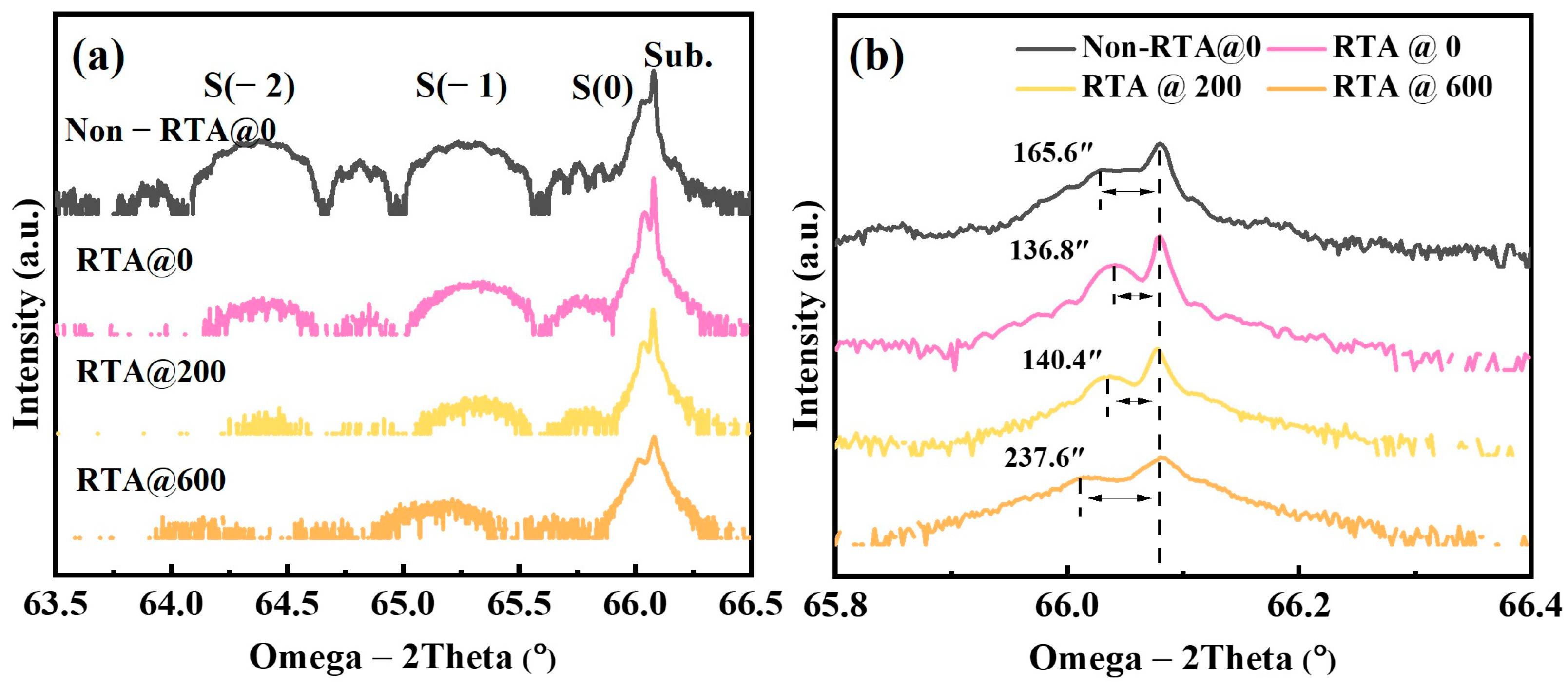
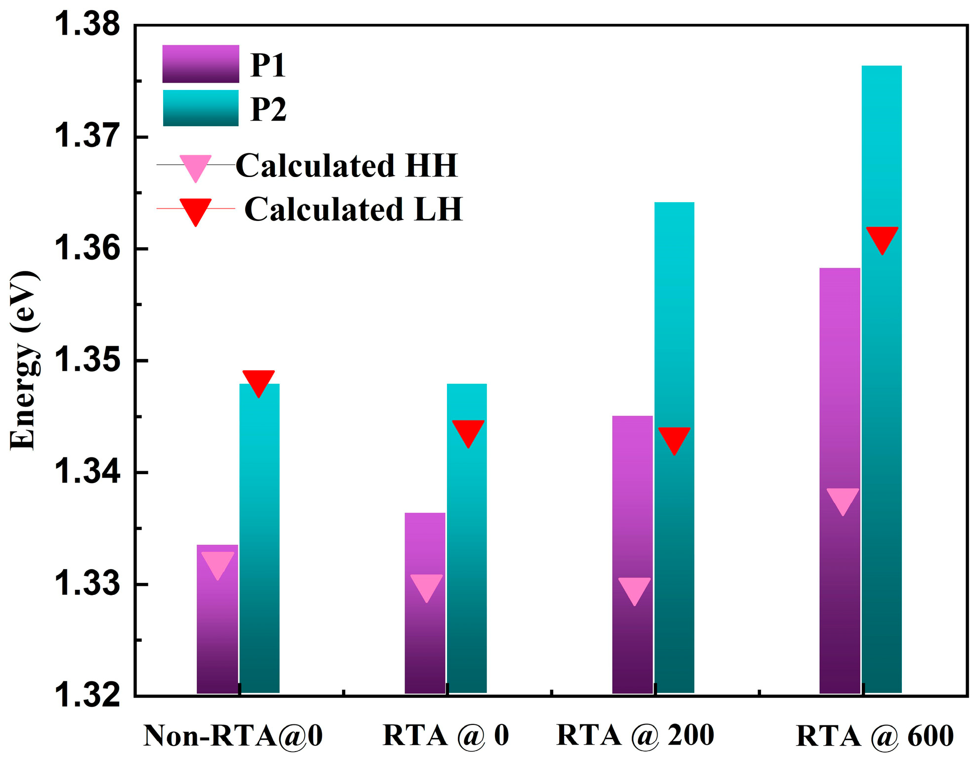
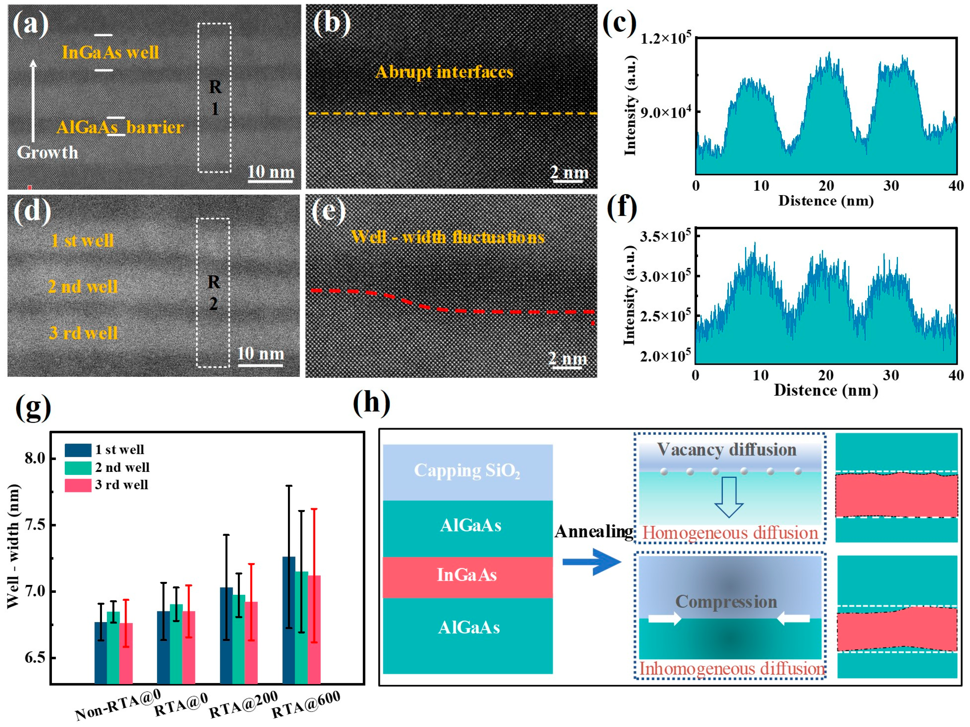
3. Results and Discussion

Prior to discussing the experimental results, taking into account the theoretical energy band structure of the fabricated samples facilitates the understanding of the photogenerated carriers’ exact optical transitions. The Nextnano++ 3.1.0 software was employed to simulate the properties of the MQW materials under 300 k conditions, including band-edge band structure, electron–hole localization, and strain, based on the structural parameters of the InGaAs/AlGaAs MQWs grown as in Figure 1. The material parameters of GaAs, InAs, and AlAs, including Eg and the electron effective mass, were taken from the database that comes with the software, and Vegard’s theorem was employed to calculate the energy-band edge structure of the well-layered and barrier-layered ternary alloys. The energy band shifts between the well and barrier layers were obtained through simulations based on a self-consistent solution of the Schrödinger equation taking into account the effect of band-edge shifts induced by the InGaAs/AlGaAs strain, as shown in Figure 2. In addition, the strain also plays an important role in separating the subband energies of the quantum wells. For InGaAs/AlGaAs MQWs, the compressive strain increases the compressive strain by more than 1.0%, and the valence interband and splitting are the key factors affecting the position of the HH and LH band edges.
The normalized PL intensity spectra of the fabricated samples are shown in Figure 3 for comparison. Based on the Gaussian fitting curves, the emission spectra of all samples consisted of three components, where the transition energies of the main and shoulder peaks are related to the valence band splitting of the heavy hole (HH) band and light hole (LH) band generated by quantum confinement. The main peak (P1) is associated with the radiative recombination of ground-state electrons and heavy holes, and the shoulder peak (P2) is related to the radiative recombination of ground-state electrons and light holes [24]. The peak (P3) located at ~1.425 eV is considered as the PL peak of the GaAs substrate material. From Figure 3, we can see the blueshift behavior of the InGaAs/AlGaAs MQWs after annealing as their emission peak with the SiO2 capping layer shifted from 1.333 eV to 1.361 eV compared with the non-capped samples. Additionally, on increasing the SiO2 thickness from 0 nm to 600 nm, the full width at the half-maximum (FWHM) of the PL spectrum was found to be broadened from 8.7 meV to 25.9 meV. It can also be observed that the unnormalized PL intensity signal of all the annealed coating samples became weaker. Firstly, group III vacancies were created at the GaAs–SiO2 interface due to the out-diffusion of Ga atoms into the dielectric capping layer [16]. The group III vacancy diffused into the QW region, promoted the atomic interdiffusion between the barrier and the well, and therefore, led to the PL peak shift toward the higher-energy side. Secondly, due to the difference in thermal expansion coefficients between SiO2 (5.2 × 10⁻⁷ °C−1) and GaAs (6.86 × 10⁻⁶ °C−1) by an order of magnitude, compressive stress was generated at the GaAs/SiO2 interface to affect the emission wavelength during the annealing process [25,26]. Thirdly, as the compressive strain increased, the conduction-band edge grew and the valence-band edges shrank conversely; consequently, the bandgap became wider, and the emission peaks tended to display a large blueshift. Thus, the blueshift of the bandgap is related to the changes in material composition as well as the induced strain during the intermixing process. The broadening and weakening of the emission peak can be attributed to the nonradiative recombination effect caused by the QW structural disorder. It can be demonstrated that the blueshift behavior of the InGaAs/AlGaAs MQWs can be effectively enhanced by increasing the thickness of the SiO2 capping layer.
To verify the effect of interfacial atomic diffusion on the microstructure and photoluminescence properties of InGaAs/AlGaAs MQWs, all samples were measured using PL at 77 K; the results are shown in Figure 4. The peak intensity of sample RTA@0 was slightly lower as compared to that of sample Non-RTA@0, and the PL peak position was nearly unchanged. In general, the diffusion of atoms at the quantum-well interface was not activated by a short rapid annealing. In contrast, the intensity of the RTA@600 sample decreased rapidly and the half-width more than doubled under the same thermal treatment conditions. Atom diffusion at the quantum-well interface disrupts the atomic structure of the quantum well and increases the interface alloy disorder, which increases the scattering chance of carriers. The results of the 77 K PL further confirm that the introduction of the SiO2 layer can effectively enhance the mixing of interfacial atoms to tune the quantum emission wavelength.
The variations in the structural characteristics and strain of the annealed MQWs with different thicknesses of SiO2 capping layers were investigated through the HRXRD spectrum, as illustrated in Figure 5. The observed clear interference fringes in the Non-RTA@0 sample suggest that these MQWs maintained excellent interfacial crystal quality and periodicity. For all annealed samples, the intensity of the satellite peak decreased and was accompanied by the disappearance of the secondary satellite peak, which indicated the slight degradation of the abrupt interface of the InGaAs/AlGaAs MQWs. Moreover, the level-zero satellite peaks of the annealed samples moved closer to and then further away from the GaAs substrate peaks based on the increasing thickness of the dielectric coatings, which means that the strain of the MQWs changed. The values of the zeroth-order satellite peak away from the GaAs peak for the four samples were 165.6, 136.8, 140.4, and 237.6 arc-seconds, respectively. The quantitative interfacial strain value in the InGaAs/AlGaAs MQWs can be calculated using the following formula [27]:
ε = c o t θ e θ
where ε is the actual strain of the InGaAs/AlGaAs MQWs, θ e is the Bragg angle of the GaAs substrate, and θ is the separation between the zeroth-order satellite peak and the GaAs substrate [28]. Then, the actual strain in the four samples was −1.23 × 10⁻³, −1.05 × 10⁻³, −1.02 × 10⁻³, and −1.77 × 10⁻³, respectively; here, the negative sign accounts for compressive strain. For the RTA@0 sample, the strain was significantly degraded compared with that of the Non-RTA@0 sample, which can be interpreted as the relief of the annealed strain. In contrast, the increased strain in the RTA@600 sample can be considered the result of the competition between the strain introduced by both the SiO2 capping and the relief stress during the annealing process [29]. As mentioned above, it was found that the atomic intermixing at the strain-enhanced interface was the main reason for the strain variation and the disappearance of the satellite peaks.
In order to theoretically investigate the energy bandgap blueshift mechanism under induced interfacial strain, quantitative calculations were carried out, taking quantum confinement effect into account, to determine the relationship between the emission peak blueshift and the strain. The conduction band of heavy holes (HHs) and light holes (LHs) in the InGaAs well layer under the strain condition were obtained using the following equations [30]:
E c H H = E 0 I n x G a 1 x A s + 2 a 1 C 12 C 11 ε b 1 + 2 C 12 C 11 ε
E c L H = E 0 I n x G a 1 x A s + 2 a 1 C 12 C 11 ε + b 1 + 2 C 12 C 11 ε
a = a c a v
where E0(InxGa1−xAs) is the unstrained bandgap of the bulk InGaAs material, assuming that the InGaAs bandgap at 300 k follows the relation E0(x) = (1.422 − 1.53x + 0.45x2)eV, where x is the indium mole fraction [31]. Moreover, ac and av are the conduction- and valence-band deformation states, b is the shear deformation state, C11 and C12 are the elastic-stiffness constants; their offsets relative to the indium content were calculated through linear interpolation as described in Refs. [32,33,34]. Considering the effect of quantum confinement on the transition energy level of the carrier, the values of HHs and LHs in the well were calculated using the Schrodinger equation according to the boundary conditions of the wave function. Based on the above equations, the obtained transition energy levels of HHs and LHs at 300 k are plotted in Figure 6.
The theoretical calculated values of all the annealed samples were smaller than the corresponding experimental results (Figure 6). In addition, the wavelengths obtained based on the elastic strain theory exhibited a trend of redshift and then blueshift as the thickness of the SiO2 capping layer increased. For RTA@200, although the actual strain was almost the same as that of RTA@0, its emission peak had a relatively larger blueshift than the experimental tested results. In general, the intermixing rate in the MQWs mainly depends on the diffusivity and concentration of group III vacancies. The strain in RTA@200 was insufficient to generate a significant band shift; therefore, the principal factor for the blueshift was the increasing number of cation vacancies caused by the SiO2 capping. Notably, an obvious blueshift phenomenon in the RTA@600 sample with a thicker capping layer was observed due to the interfacial-strain-induced enhancement of the bandgap in the InGaAs/AlGaAs MQWs.
To figure out the interfacial microstructure and quality of the InGaAs/AlGaAs MQWs with a higher resolution, high-angle annular dark field (HAADF) images were plotted. Figure 7a,d show the cross-sectional HAADF images of the Non-RTA@0 and RTA@600 samples, respectively. As can be observed, the well layer and barrier layer in the as-grown sample were neatly arranged as a high-quality abrupt interface. Compared to Figure 7b, the wells fluctuated significantly, and their interfaces became gradually blurred in Figure 7e (RTA@600 nm). Figure 7c,f show the atomic column intensity profiles curves along the growth direction in the Non-RTA@0 and RTA@600 samples, respectively. These profiles show that the intensity contrast oscillations between the wells and barriers were gradually flattening, indicating that the compositional variations between the wells and barriers turned from an abrupt distribution to a gradient distribution. In addition, the well-width fluctuation penetrated from the surface to the inside of the active region and propagated vertically through the entire quantum-well structure. We expect that the width fluctuation may be caused by the nonuniform diffusion of atoms between the well–barrier interfaces. As illustrated in Figure 7g, the modulation amplitudes of the well thickness tended to decrease from the surface to the penetration direction of the substrate. Generally, the expansion of the well width causes the redshift of the PL spectrum to a certain degree; however, the diversities of the barrier and well components due to atomic diffusion and the bandgap modifications caused by the interfacial strain are also important factors affecting the PL luminescence properties. Finally, the thickness fluctuations reflect the deterioration of the optical and interfacial quality, and this is responsible for the degradation of the HRXRD satellite peaks and PL intensity.
The influences of the high-temperature annealing process on the InGaAs/AlGaAs MQWs can be categorized into interdiffusion and strain effects, with the schematics of well-width fluctuation illustrated in Figure 7h. Regarding the interdiffusion effects, during the high-temperature annealing process, the vacancy on the GaAs surface diffuses into the QW region, leading to a decrease in the amplitude distribution of the barrier-width fluctuation, while the upper QW interface appears rougher than the lower interface. Considering the strain effects, the thermal expansion coefficient mismatch between the SiO2 capping layer and the GaAs layer induces a high strain field gradient, whereas the strain field perpendicular to the growth direction exerts stress on the quantum well and distorts the striations in the QW region. Based on the above reasons, the induced strain and the inhomogeneous diffusion of vacancies are responsible for the blurring of the interface and the gradient distribution of well-width fluctuations.

4. Conclusions

In summary, we systematically explored the influences of the thickness of an SiO2 capping layer on the PL properties and interfacial structural characteristics of InGaAs/AlGaAs MQWs. According to the tested results, the wavelength blueshift amplitude of the annealed MQWs improved on the increase of the capping thickness, which indicates that the interfacial strain introduced by the thermal mismatch between the dielectric layer and the semiconductor can not only enhance the interfacial atomic intermixing but also further improve the tunability of the PL peak for MQWs. Moreover, the inhomogeneous atomic diffusion during the propagation of interfacial strain led to the degradation of the interfacial quality, which was also confirmed by the variation in well-width fluctuation observed in the HAADF images and XRD patterns after annealing treatment. Therefore, the studied findings demonstrated the relationships among introduced strain, PL properties, and interfacial structure during interface mixing, which provides a new idea for the development of wavelength-tunable photonic integration devices with excellent performances in the semiconductor field.

Author Contributions

Z.Y. and S.Z. contributed equally to this work. Z.Y.: investigation, writing—original draft, data curation. S.Z.: methodology, conceptualization, investigation. S.M.: supervision, writing—review and editing. Y.S.: formal analysis. Q.L.: methodology. X.H.: methodology. L.S.: formal analysis. B.H.: methodology. B.Q.: formal analysis. B.X.: supervision, writing—review and editing, funding acquisition. All authors have read and agreed to the published version of the manuscript.

Funding

This research was funded by National Natural Science Foundation of China (21972103) and the SHANXI-ZHEDA Institute of Advanced Materials and Chemical Engineering (2021SX-AT007).

Institutional Review Board Statement

Not applicable.

Informed Consent Statement

Not applicable.

Data Availability Statement

The data used to support the findings of this study are available from the corresponding author upon request.

Conflicts of Interest

The authors declare that they have no conflict of interest.

References

  1. Yu, J.S.; Song, J.D.; Lee, Y.T.; Lim, H. Effects of rapid thermal annealing on the optical properties of In0.53Ga0.47As/In0.52Al0.48As multiple quantum wells with InGaAs and dielectric capping layers. J. Appl. Phys. 2002, 91, 2080–2084. [Google Scholar] [CrossRef]
  2. Taniguchi, H.; Ishii, H.; Minato, R.; Ohki, Y.; Namegaya, T.; Kasukawa, A. 25-W 915-nm lasers with window structure fabricated by impurity-free vacancy disordering (IFVD). IEEE J. Sel. Top. Quantum Electron. 2007, 13, 1176–1179. [Google Scholar] [CrossRef]
  3. Yu, J.; Song, J.; Lee, Y.; Lim, H. Fabrication of multi-wavelength In0.2Ga0.8As/GaAs multiple quantum well laser diodes by area-selective impurity-free vacancy disordering using SiOx capping layers with different stoichiometries. Appl. Phys. A 2005, 80, 847–850. [Google Scholar] [CrossRef]
  4. Vostokov, N.; Revin, M.; Shashkin, I.S. Microwave detector diodes based on InGaAs/AlGaAs/GaAs heterostructures. J. Appl. Phys. 2020, 127, 044503. [Google Scholar] [CrossRef]
  5. Zucker, J.; Tell, B.; Jones, K.; Divino, M.; Brown-Goebeler, K.; Joyner, C.; Miller, B.; Young, M. Large blueshifting of InGaAs/InP quantum-well band gaps by ion implantation. Appl. Phys. Lett. 1992, 60, 3036–3038. [Google Scholar] [CrossRef]
  6. Djie, H.S.; Mei, T. Plasma-induced quantum well intermixing for monolithic photonic integration. IEEE J. Sel. Top. Quantum Electron. 2005, 11, 373–382. [Google Scholar] [CrossRef]
  7. Wolf, T.; Shieh, C.L.; Engelmann, R.; Alavi, K.; Mantz, J. Lateral refractive index step in GaAs/AlGaAs multiple quantum well waveguides fabricated by impurity-induced disordering. Appl. Phys. Lett. 1989, 55, 1412–1414. [Google Scholar] [CrossRef]
  8. Marsh, J.H.; Cusumano, P.; Bryce, A.C.; Ooi, B.S.; Ayling, S.G. GaAs/AlGaAs photonic integrated circuits fabricated using impurity-free vacancy disordering. In Functional Photonic Integrated Circuits; SPIE: Bellingham, WA, USA, 1995; pp. 74–85. [Google Scholar]
  9. Yu, J.S.; Song, J.D.; Lee, Y.T.; Lim, H. Influence of dielectric deposition parameters on the In0.2Ga0.8As/GaAs quantum well intermixing by impurity-free vacancy disordering. J. Appl. Phys. 2002, 92, 1386–1390. [Google Scholar] [CrossRef]
  10. Zhongliang, Q.; Xiaohong, T.; Kenneth, L.E.K.; Huei, L.P.; BaoXue, B. Large energy band-gap tuning of 980 nm InGaAs/InGaAsP quantum well structure via quantum well intermixing. Solid-State Electron. 2013, 79, 281–284. [Google Scholar] [CrossRef]
  11. Hulko, O.; Thompson, D.A.; Simmons, J.G. Comparison of quantum well interdiffusion on group III, group V, and combined groups III and V sublattices in GaAs-based structures. IEEE J. Sel. Top. Quantum Electron. 2008, 14, 1104–1112. [Google Scholar] [CrossRef]
  12. Ludewig, P.; Reinhard, S.; Jandieri, K.; Wegele, T.; Beyer, A.; Tapfer, L.; Volz, K.; Stolz, W. MOVPE growth studies of Ga (NAsP)/(BGa)(AsP) multi quantum well heterostructures (MQWH) for the monolithic integration of laser structures on (001) Si-substrates. J. Cryst. Growth. 2016, 438, 63–69. [Google Scholar] [CrossRef]
  13. Wegele, T.; Beyer, A.; Ludewig, P.; Rosenow, P.; Duschek, L.; Jandieri, K.; Tonner, R.; Stolz, W.; Volz, K. Interface morphology and composition of Ga(NAsP) quantum well structures for monolithically integrated LASERs on silicon substrates. J. Phys. D Appl. Phys. 2016, 49, 075108. [Google Scholar] [CrossRef]
  14. Mitsuhara, M.; Ogasawara, M.; Sugiura, H. Effect of strain in the barrier layer on structural and optical properties of highly strained In0.77Ga0.23As/InGaAs multiple quantum wells. J. Cryst. Growth. 2000, 210, 463–470. [Google Scholar] [CrossRef]
  15. Ryu, S.W.; Kim, I.; Choe, B.D.; Jeong, W.G. The effect of strain on the interdiffusion in InGaAs/GaAs quantum wells. Appl. Phys. Lett. 1995, 67, 1417–1419. [Google Scholar] [CrossRef]
  16. Gareso, P.; Tan, H.H.; Jagadish, C. Impurity Free Vacancy Disordering (IFVD) of InGaAs/AlGaAs Quantum Well Laser Structures. ECS J. Solid State Sci. 2017, 6, N122. [Google Scholar] [CrossRef]
  17. Al-Jabr, A.; Majid, M.A.; Alias, M.S.; Anjum, D.H.; Ng, T.K.; Ooi, B.S. Large bandgap blueshifts in the InGaP/InAlGaP laser structure using novel strain-induced quantum well intermixing. J. Appl. Phys. 2016, 119, 135703. [Google Scholar] [CrossRef]
  18. Wang, X.; Cui, X.; Bhat, A.; Savage, D.E.; Reno, J.L.; Lagally, M.G.; Paiella, R. Ultrawide strain-tuning of light emission from InGaAs nanomembranes. Appl. Phys. Lett. 2018, 113, 201105. [Google Scholar] [CrossRef]
  19. Gareso, P.; Buda, M.; Fu, L.; Tan, H.; Jagadish, C. Influence of SiO2 and TiO2 dielectric layers on the atomic intermixing of InxGa1−xAs/InP quantum well structures. Semicond. Sci. Technol. 2007, 22, 988. [Google Scholar] [CrossRef]
  20. Hao, X.; Li, L.; Kong, Q.; Ma, S.; Wang, J.; Xu, Y.; Liu, X.; Han, B.; Qiu, B.; Xu, B. Atomic-scale insights of the effect of growth temperature on the migration behavior of Al atoms in InGaAs/AlGaAs multiple quantum wells. Mater. Sci. Semicond. Process. 2023, 154, 107197. [Google Scholar] [CrossRef]
  21. Liu, Q.; Han, D.; Ma, S.; Hao, X.; Wei, Y.; Cao, B.; Zhang, S.; Hou, Y.; Shang, L.; Han, B.; et al. Effect of in situ degradation on the atomic structure and optical properties of GaN-based green light-emitting diodes. Appl. Phys. Lett. 2020, 117, 212103. [Google Scholar] [CrossRef]
  22. Liu, Q.; Han, D.; Shang, L.; Hao, X.; Hou, Y.; Zhang, S.; Cao, B.; Han, B.; Shan, H.; Yang, Y.; et al. Effect of V-Shaped pits on optical properties of GaN-Based green light-emitting diodes. Opt. Mater. 2020, 107, 110129. [Google Scholar] [CrossRef]
  23. Ma, S.; Li, L.; Kong, Q.; Xu, Y.; Liu, Q.M.; Zhang, S.; Zhang, X.; Han, B.; Qiu, B.; Xu, B.; et al. Atomic-scale insights of indium segregation and its suppression by GaAs insertion layer in InGaAs/AlGaAs multiple quantum wells. Chin. Phys. B 2022, 32, 037801. [Google Scholar] [CrossRef]
  24. Zhang, B.; Wang, H.; Wang, X.; Wang, Q.; Fan, J.; Zou, Y.; Ma, X. Effect of GaAs insertion layer on the properties improvement of InGaAs/AlGaAs multiple quantum wells grown by metal-organic chemical vapor deposition. J. Alloys Compd. 2021, 872, 159470. [Google Scholar] [CrossRef]
  25. Fu, L.; Wong-Leung, J.; Deenapanray, P.; Tan, H.; Jagadish, C.; Gong, B.; Lamb, R.; Cohen, R.; Reichert, W.; Dao, L. Suppression of interdiffusion in GaAs/AlGaAs quantum-well structure capped with dielectric films by deposition of gallium oxide. J. Appl. Phys. 2002, 92, 3579–3583. [Google Scholar] [CrossRef]
  26. Ooi, B.S.; McIlvaney, K.; Street, M.W.; Helmy, A.S.; Ayling, S.G.; Bryce, A.C.; Marsh, J.H.; Roberts, J. Selective quantum-well intermixing in GaAs-AlGaAs structures using impurity-free vacancy diffusion. IEEE J. Quantum Electron. 1997, 33, 1784–1793. [Google Scholar]
  27. Seo, J.H.; Seo, K.S. Strain relaxation of InGaAs/GaAs superlattices by wet oxidation of underlying AlAs layer. Appl. Phys. Lett. 1998, 72, 1466–1468. [Google Scholar] [CrossRef]
  28. Sarıkavak, B.; Öztürk, M.; Mammadov, T.; Özçelik, S. Interdiffusion phenomena in InGaAs/GaAs superlattice structures. Cryst. Res. Technol. 2010, 45, 517–524. [Google Scholar] [CrossRef]
  29. Liu, S.; Yang, J.; Zhao, D.; Jiang, D.; Liang, F.; Chen, P.; Zhu, J.; Liu, Z.; Liu, W.; Xing, Y. The influence of thermal annealing process after GaN cap layer growth on structural and optical properties of InGaN/InGaN multi-quantum wells. Opt. Mater. 2018, 86, 460–463. [Google Scholar] [CrossRef]
  30. Vurgaftman, I.; Meyer, J.Á.; Ram-Mohan, L.Á. Band parameters for III–V compound semiconductors and their alloys. J. Appl. Phys. 2001, 89, 5815–5875. [Google Scholar] [CrossRef]
  31. Kudo, M.; Mishima, T. Improved photoluminescence properties of highly strained InGaAs/GaAs quantum wells grown by molecular-beam epitaxy. J. Appl. Phys. 1995, 78, 1685–1688. [Google Scholar] [CrossRef]
  32. Minch, J.; Park, S.; Keating, T.; Chuang, S. Theory and experiment of InGaAsP and InGaAlAs long-wavelength strained quantum-well lasers. IEEE J. Quantum Electron. 1999, 35, 771–782. [Google Scholar] [CrossRef]
  33. Jensen, J.R.; Hvam, J.M.; Langbein, W. Optical properties of InAlGaAs quantum wells: Influence of segregation and band bowing. J. Appl. Phys. 1999, 86, 2584–2589. [Google Scholar] [CrossRef]
  34. Micallef, J.; Li, E.H.; Weiss, B.L. The effects of strain on the confinement profile of disordered InGaAs/GaAs single quantum wells. Superlattices Microstruct. 1993, 13, 125–132. [Google Scholar] [CrossRef]
Figure 1. InGaAs/AlGaAs MQW sample with SiO2 capping layer and the atomic interdiffusion process at the barrier–well interfaces under high-temperature annealing.
Materials 16 06068 g001
Figure 2. Nextnano++ (a) energy band structure, electron–hole energy levels and (b) elastic strain simulations of as-grown sample at 300 k. The Ec, Ev, Ee1, Ehh1, and Elh1 are the energies of the conduction band, the valence band, the electronic ground state, and the heavy and light hole bands, respectively.
Materials 16 06068 g002
Figure 3. The room-temperature PL spectra and Gaussian fitting curves for (a) Non-RTA@0, (b) RTA@0, (c) RTA@200, (d) RTA@600.
Materials 16 06068 g003
Figure 4. The PL curves for all samples measured under 77 k conditions. The inset graph illustrates the variations in the FWHM of the PL curves for each of the samples.
Materials 16 06068 g004
Figure 5. (a) HRXRD ω/2θ (004) scans of the MQWs, (b) substrate and zeroth-order satellite peaks of enlarged areas.
Materials 16 06068 g005
Figure 6. The evolution of P1, P2 and the calculated values of HH and LH emission for different samples. The triangle symbols are calculated results for InGaAs/AlGaAs MQWs.
Materials 16 06068 g006
Figure 7. Cross-sectional HAADF images of the samples (a,b) Non-RTA@0 and (d,e) RTA@600. The higher magnifications of the white boxes in figure (a,d) are displayed in (c,f). (g) The average thicknesses of different well layers in the samples were measured at 10 different areas; the error bar represents the standard deviation of the well width. (h) Well-layer shape deformation in InGaAs/AlGaAs MQWs.
Materials 16 06068 g007
Disclaimer/Publisher’s Note: The statements, opinions and data contained in all publications are solely those of the individual author(s) and contributor(s) and not of MDPI and/or the editor(s). MDPI and/or the editor(s) disclaim responsibility for any injury to people or property resulting from any ideas, methods, instructions or products referred to in the content.

