
High-Entropy Perovskite Thin Film in the Gd-Nd-Sm-La-Y-Co System: Deposition, Structure and Optoelectronic Properties

 , , , , ,
  , and
, and
Abstract
:
1. Introduction
2. Materials and Methods
3. Results and Discussion
4. Conclusions
Author Contributions
Funding
Institutional Review Board Statement
Informed Consent Statement
Data Availability Statement
Acknowledgments
Conflicts of Interest
References
- Ye, Y.F.; Wang, Q.; Lu, J.; Liu, C.T.; Yang, Y. High-Entropy Alloy: Challenges and Prospects. Mater. Today 2016, 19, 349–362. [Google Scholar] [CrossRef]
- Rost, C.M.; Sachet, E.; Borman, T.; Moballegh, A.; Dickey, E.C.; Hou, D.; Jones, J.L.; Curtarolo, S.; Maria, J.-P. Entropy-Stabilized Oxides. Nat. Commun. 2015, 6, 8485. [Google Scholar] [CrossRef] [PubMed] [Green Version]
- Dąbrowa, J.; Stygar, M.; Mikuła, A.; Knapik, A.; Mroczka, K.; Tejchman, W.; Danielewski, M.; Martin, M. Synthesis and Microstructure of the (Co,Cr,Fe,Mn,Ni)3O4 High Entropy Oxide Characterized by Spinel Structure. Mater. Lett. 2018, 216, 32–36. [Google Scholar] [CrossRef]
- Djenadic, R.; Sarkar, A.; Clemens, O.; Loho, C.; Botros, M.; Chakravadhanula, V.S.K.; Kübel, C.; Bhattacharya, S.S.; Gandhi, A.S.; Hahn, H. Multicomponent Equiatomic Rare Earth Oxides. Mater. Res. Lett. 2017, 5, 102–109. [Google Scholar] [CrossRef] [Green Version]
- Oses, C.; Toher, C.; Curtarolo, S. High-Entropy Ceramics. Nat. Rev. Mater. 2020, 5, 295–309. [Google Scholar] [CrossRef]
- Zhang, R.-Z.; Reece, M.J. Review of High Entropy Ceramics: Design, Synthesis, Structure and Properties. J. Mater. Chem. A 2019, 7, 22148–22162. [Google Scholar] [CrossRef] [Green Version]
- Yeh, J.-W.; Chen, S.-K.; Lin, S.-J.; Gan, J.-Y.; Chin, T.-S.; Shun, T.-T.; Tsau, C.-H.; Chang, S.-Y. Nanostructured High-Entropy Alloys with Multiple Principal Elements: Novel Alloy Design Concepts and Outcomes. Adv. Eng. Mater. 2004, 6, 299–303. [Google Scholar] [CrossRef]
- Bała, P.; Górecki, K.; Bednarczyk, W.; Wątroba, M.; Lech, S.; Kawałko, J. Effect of High-Temperature Exposure on the Microstructure and Mechanical Properties of the Al5Ti5Co35Ni35Fe20 High-Entropy Alloy. J. Mater. Res. Technol. 2020, 9, 551–559. [Google Scholar] [CrossRef]
- High-Entropy Alloys—2nd Edition. Available online: https://www.elsevier.com/books/high-entropy-alloys/murty/978-0-12-816067-1 (accessed on 13 May 2023).
- Rost, C.M. Entropy-Stabilized Oxides: Explorations of a Novel Class of Multicomponent Materials. Ph.D. thesis, North Carolina State University, Raleigh, NC, USA, 2016. [Google Scholar]
- Zhang, Y.; Zhang, Z.; Wang, X.; Yao, W.; Liang, X. Structure and Properties of High-Entropy Amorphous Thin Films: A Review. JOM 2022, 74, 794–807. [Google Scholar] [CrossRef]
- Zheng, Y.; Zou, M.; Zhang, W.; Yi, D.; Lan, J.; Nan, C.-W.; Lin, Y.-H. Electrical and Thermal Transport Behaviours of High-Entropy Perovskite Thermoelectric Oxides. J. Adv. Ceram. 2021, 10, 377–384. [Google Scholar] [CrossRef]
- Ferro, S.M.; Wobben, M.; Ehrler, B. Rare-Earth Quantum Cutting in Metal Halide Perovskites—A Review. Mater. Horiz. 2021, 8, 1072–1083. [Google Scholar] [CrossRef]
- Dhole, S.; Chen, A.; Nie, W.; Park, B.; Jia, Q. Strain Engineering: A Pathway for Tunable Functionalities of Perovskite Metal Oxide Films. Nanomaterials 2022, 12, 835. [Google Scholar] [CrossRef] [PubMed]
- Corey, Z.J.; Lu, P.; Zhang, G.; Sharma, Y.; Rutherford, B.X.; Dhole, S.; Roy, P.; Wang, Z.; Wu, Y.; Wang, H.; et al. Structural and Optical Properties of High Entropy (La,Lu,Y,Gd,Ce)AlO3 Perovskite Thin Films. Adv. Sci. 2022, 9, 2202671. [Google Scholar] [CrossRef]
- Uehara, M.; Mori, S.; Chen, C.-L.; Cheong, S.-W. Percolative Phase Separation Underlies Colossal Magnetoresistance in Mixed-Valent Manganites. Nature 1999, 399, 560–563. [Google Scholar] [CrossRef]
- Dagotto, E.; Hotta, T.; Moreo, A. Colossal Magnetoresistant Materials: The Key Role of Phase Separation. Phys. Rep. 2001, 344, 1–153. [Google Scholar] [CrossRef] [Green Version]
- Bresolin, B.-M.; Park, Y.; Bahnemann, D.W. Recent Progresses on Metal Halide Perovskite-Based Material as Potential Photocatalyst. Catalysts 2020, 10, 709. [Google Scholar] [CrossRef]
- Tabish, A.; Varghese, A.M.; Wahab, M.A.; Karanikolos, G.N. Perovskites in the Energy Grid and CO2 Conversion: Current Context and Future Directions. Catalysts 2020, 10, 95. [Google Scholar] [CrossRef] [Green Version]
- Górecki, K.; Bała, P.; Bednarczyk, W.; Kawałko, J. Cryogenic Behaviour of the Al5Ti5Co35Ni35Fe20 Multi-Principal Component Alloy. Mater. Sci. Eng. A 2019, 745, 346–352. [Google Scholar] [CrossRef]
- Taniguchi, Y.; Li, H.-B.; Hattori, A.N.; Tanaka, H. Comprehensive Determination of Proton Diffusion in Protonated NdNiO3 Thin Film by a Combination of Electrochemical Impedance Spectroscopy and Optical Observation. Appl. Phys. Express 2023, 16, 035501. [Google Scholar] [CrossRef]
- Qi, H.; Chen, L.; Deng, S.; Chen, J. High-Entropy Ferroelectric Materials. Nat. Rev. Mater. 2023, 8, 355–356. [Google Scholar] [CrossRef]
- Kante, M.V.; Weber, M.L.; Ni, S.; van den Bosch, I.C.G.; van der Minne, E.; Heymann, L.; Falling, L.J.; Gauquelin, N.; Tsvetanova, M.; Cunha, D.M.; et al. A High-Entropy Oxide as High-Activity Electrocatalyst for Water Oxidation. ACS Nano 2023, 17, 5329–5339. [Google Scholar] [CrossRef] [PubMed]
- Esquius, J.R.; Liu, L. High Entropy Materials as Emerging Electrocatalysts for Hydrogen Production through Low-Temperature Water Electrolysis. Mater. Futures 2023, 2, 022102. [Google Scholar] [CrossRef]
- Tu, J.; Ding, J.; Xi, G.; Li, H.; Yang, Q.; Tian, J.; Zhang, L. Controllable Chemical Composition in Double-Perovskite Bi0.5Sm0.5FeO3 Epitaxial Thin Films for Ferroelectric, Photovoltaic, and Ferromagnetic Properties. Chem. Eng. J. 2023, 453, 139726. [Google Scholar] [CrossRef]
- Liu, Z.; Tang, Z.; Song, Y.; Yang, G.; Qian, W.; Yang, M.; Zhu, Y.; Ran, R.; Wang, W.; Zhou, W.; et al. High-Entropy Perovskite Oxide: A New Opportunity for Developing Highly Active and Durable Air Electrode for Reversible Protonic Ceramic Electrochemical Cells. Nano-Micro Lett. 2022, 14, 217. [Google Scholar] [CrossRef]
- Vinnik, D.A.; Zhivulin, V.E.; Trofimov, E.A.; Gudkova, S.A.; Punda, A.Y.; Valiulina, A.N.; Gavrilyak, M.; Zaitseva, O.V.; Taskaev, S.V.; Khandaker, M.U.; et al. A-Site Cation Size Effect on Structure and Magnetic Properties of Sm(Eu,Gd)Cr0.2Mn0.2Fe0.2Co0.2Ni0.2O3 High-Entropy Solid Solutions. Nanomaterials 2022, 12, 36. [Google Scholar] [CrossRef]
- Goko, T.; Arguello, C.J.; Hamann, A.; Wolf, T.; Lee, M.; Reznik, D.; Maisuradze, A.; Khasanov, R.; Morenzoni, E.; Uemura, Y.J. Restoration of Quantum Critical Behavior by Disorder in Pressure-Tuned (Mn,Fe)Si. npj Quantum Mater. 2017, 2, 44. [Google Scholar] [CrossRef] [Green Version]
- Sales, B.C.; Jin, K.; Bei, H.; Stocks, G.M.; Samolyuk, G.D.; May, A.F.; McGuire, M.A. Quantum Critical Behavior in a Concentrated Ternary Solid Solution. Sci. Rep. 2016, 6, 26179. [Google Scholar] [CrossRef] [Green Version]
- Chen, Q.; Han, T.; Zeng, J.; He, Z.; Liu, Y.; Sun, J.; Tang, M.; Zhang, Z.; Gao, P.; Liu, G. Perovskite-Based Memristor with 50-Fold Switchable Photosensitivity for In-Sensor Computing Neural Network. Nanomaterials 2022, 12, 2217. [Google Scholar] [CrossRef]
- Zeng, F.; Guo, Y.; Hu, W.; Tan, Y.; Zhang, X.; Feng, J.; Tang, X. Opportunity of the Lead-Free All-Inorganic Cs3Cu2I5 Perovskite Film for Memristor and Neuromorphic Computing Applications. ACS Appl. Mater. Interfaces 2020, 12, 23094–23101. [Google Scholar] [CrossRef] [PubMed]
- Lee, K.; Han, H.; Park, C. Nanostructured Perovskites for Retina-Inspired Structurally Tunable Synapse. In Proceedings of the International Conference on Perovskite Memristors and Electronics 2021 (ICPME2021), Online, 13–14 December 2021. [Google Scholar] [CrossRef]
- Huang, X.; Guo, Y.; Liu, Y. Perovskite Photodetectors and Their Application in Artificial Photonic Synapses. Chem. Commun. 2021, 57, 11429–11442. [Google Scholar] [CrossRef] [PubMed]
- Chen, J.; Tang, X.; Liu, Q.; Jiang, Y.; Zhong, W.; Luo, F. An Artificial Synapse Based on CsPbI3 Thin Film. Micromachines 2022, 13, 284. [Google Scholar] [CrossRef] [PubMed]
- Choi, J.; Han, J.S.; Hong, K.; Kim, S.Y.; Jang, H.W. Organic–Inorganic Hybrid Halide Perovskites for Memories, Transistors, and Artificial Synapses. Adv. Mater. 2018, 30, 1704002. [Google Scholar] [CrossRef] [PubMed]
- Patel, R.K.; Ojha, S.K.; Kumar, S.; Saha, A.; Mandal, P.; Freeland, J.W.; Middey, S. Epitaxial Stabilization of Ultra Thin Films of High Entropy Perovskite. Appl. Phys. Lett. 2020, 116, 071601. [Google Scholar] [CrossRef] [Green Version]
- Son, Y.; Zhu, W.; Trolier-McKinstry, S.E. Electrocaloric Effect of Perovskite High Entropy Oxide Films. Adv. Electron. Mater. 2022, 8, 2200352. [Google Scholar] [CrossRef]
- Jiang, S.; Hu, T.; Gild, J.; Zhou, N.; Nie, J.; Qin, M.; Harrington, T.; Vecchio, K.; Luo, J. A New Class of High-Entropy Perovskite Oxides. Scr. Mater. 2018, 142, 116–120. [Google Scholar] [CrossRef]
- Kotsonis, G.N.; Rost, C.M.; Harris, D.T.; Maria, J.-P. Epitaxial Entropy-Stabilized Oxides: Growth of Chemically Diverse Phases via Kinetic Bombardment. MRS Commun. 2018, 8, 1371–1377. [Google Scholar] [CrossRef]
- Schlom, D.G.; Chen, L.-Q.; Pan, X.; Schmehl, A.; Zurbuchen, M.A. A Thin Film Approach to Engineering Functionality into Oxides. J. Am. Ceram. Soc. 2008, 91, 2429–2454. [Google Scholar] [CrossRef]
- Krawczyk, P.A.; Jurczyszyn, M.; Pawlak, J.; Salamon, W.; Baran, P.; Kmita, A.; Gondek, Ł.; Sikora, M.; Kapusta, C.; Strączek, T.; et al. High-Entropy Perovskites as Multifunctional Metal Oxide Semiconductors: Synthesis and Characterization of (Gd0.2Nd0.2La0.2Sm0.2Y0.2)CoO3. ACS Appl. Electron. Mater. 2020, 2, 3211–3220. [Google Scholar] [CrossRef]
- Goldschmidt, V.M. Die Gesetze der Krystallochemie. Naturwissenschaften 1926, 14, 477–485. [Google Scholar] [CrossRef]
- Zhang, Y.; Zhou, Y.J.; Lin, J.P.; Chen, G.L.; Liaw, P.K. Solid-Solution Phase Formation Rules for Multi-Component Alloys. Adv. Eng. Mater. 2008, 10, 534–538. [Google Scholar] [CrossRef]
- Jędrusik, M.; Cieniek, Ł.; Kopia, A.; Turquat, C.; Leroux, C. Structural Characterization of LaCoO3 Thin Films Grown by Pulsed Laser Deposition. Arch. Metall. Mater. 2020, 65, 793–797. [Google Scholar] [CrossRef]
- Schwarcz, D.; Burov, S. The Effect of Disordered Substrate on Crystallization in 2D. J. Phys. Condens. Matter 2019, 31, 445401. [Google Scholar] [CrossRef] [PubMed] [Green Version]
- Salaheldeen, M.; Garcia, A.; Corte-Leon, P.; Ipatov, M.; Zhukova, V.; Zhukov, A. Unveiling the Effect of Annealing on Magnetic Properties of Nanocrystalline Half-Metallic Heusler Co2FeSi Alloy Glass-Coated Microwires. J. Mater. Res. Technol. 2022, 20, 4161–4172. [Google Scholar] [CrossRef]
- Biesinger, M.; Payne, B.; Grosvenor, A.; Lau, L.; Gerson, A.; Smart, R.S.C. Resolving Surface Chemical States in XPS Analysis of First Row Transition Metals, Oxides and Hydroxides: Cr, Mn, Fe, Co and Ni. Appl. Surf. Sci. 2011, 257, 2717–2730. [Google Scholar] [CrossRef]
- Okamoto, Y.; Adachi, T.; Maezawa, A.; Imanaka, T. Effect of ZnO Addition on Cobalt–Alumina Interaction Species. Bull. Chem. Soc. Jpn. 1991, 64, 236–242. [Google Scholar] [CrossRef] [Green Version]
- Dash, K.; Folkesson, B.; Larsson, R.; Mohapatra, M. An XPS Investigation on a Series of Schiff Base Dioxime Ligands and Cobalt Complexes. J. Electron Spectrosc. Relat. Phenom. 1989, 49, 343–357. [Google Scholar] [CrossRef]
- Wagner, A.; Naumkin, A.; Kraut-Vass, A.; Allison, J.; Powell, C.; Rumble, J. NIST X-Ray Photoelectron Spectroscopy Database 1, Version 2; Natl Std. Ref. Data Series (NIST NSRDS); National Institute of Standards and Technology: Gaithersburg, MD, USA, 1997. [Google Scholar]
- Wandelt, K.; Brundle, C. The Interaction of Oxygen with Gadolinium: UPS and XPS Studies. Surf. Sci. 1985, 157, 162–182. [Google Scholar] [CrossRef]
- Uwamino, Y.; Ishizuka, T.; Yamatera, H. X-Ray Photoelectron Spectroscopy of Rare-Earth Compounds. J. Electron Spectrosc. Relat. Phenom. 1984, 34, 67–78. [Google Scholar] [CrossRef]
- Szuwarzyński, M.; Mazur, Ł.; Borkowski, M.; Maćkosz, K.; Giżyński, K.; Mazur, T. Enhanced Assembly of Ag Nanoparticles for Surface-Independent Fabrication of Conductive Patterns. ACS Appl. Nano Mater. 2022, 5, 12711–12719. [Google Scholar] [CrossRef]
- Wolski, K.; Szuwarzyński, M.; Zapotoczny, S. A Facile Route to Electronically Conductive Polyelectrolyte Brushes as Platforms of Molecular Wires. Chem. Sci. 2015, 6, 1754–1760. [Google Scholar] [CrossRef] [Green Version]
- Jarosiński, Ł.; Pawlak, J.; Al-Ani, S.K.J. Inverse Logarithmic Derivative Method for Determining the Energy Gap and the Type of Electron Transitions as an Alternative to the Tauc Method. Opt. Mater. 2019, 88, 667–673. [Google Scholar] [CrossRef]
- Cisneros, J.I. Optical Characterization of Dielectric and Semiconductor Thin Films by Use of Transmission Data. Appl. Opt. 1998, 37, 5262–5270. [Google Scholar] [CrossRef]
- Al-Ani, S.K.J.; Hogarth, C.A. The Optical Properties of Amorphous V2O5 and SiO Thin Films and of the Mixed Dielectric System SiO/V2O5. J. Mater. Sci. 1985, 20, 1185–1192. [Google Scholar] [CrossRef]
- Makuła, P.; Pacia, M.; Macyk, W. How To Correctly Determine the Band Gap Energy of Modified Semiconductor Photocatalysts Based on UV–Vis Spectra. J. Phys. Chem. Lett. 2018, 9, 6814–6817. [Google Scholar] [CrossRef] [PubMed] [Green Version]
- Kats, M.A.; Capasso, F. Optical Absorbers Based on Strong Interference in Ultra-Thin Films. Laser Photonics Rev. 2016, 10, 735–749. [Google Scholar] [CrossRef]
- Babbe, F.; Sutter-Fella, C.M. Optical Absorption-Based In Situ Characterization of Halide Perovskites. Adv. Energy Mater. 2020, 10, 1903587. [Google Scholar] [CrossRef] [Green Version]
- Lin, Y.-Y.; Gustafson, W.J.; Murray, S.E.; Shoemaker, D.P.; Ertekin, E.; Krogstad, J.A.; Perry, N.H. Perovskite Na-Ion Conductors Developed from Analogous Li3xLa2/3-xTiO3 (LLTO): Chemo-Mechanical and Defect Engineering. J. Mater. Chem. A 2021, 9, 21241–21258. [Google Scholar] [CrossRef]
- Katzbaer, R.R.; dos Santos Vieira, F.M.; Dabo, I.; Mao, Z.; Schaak, R.E. Band Gap Narrowing in a High-Entropy Spinel Oxide Semiconductor for Enhanced Oxygen Evolution Catalysis. J. Am. Chem. Soc. 2023, 145, 6753–6761. [Google Scholar] [CrossRef] [PubMed]
- Li, X.-L.; Li, Z.; Zhang, G.; Yang, G.-J. Lead-Free Perovskite [H3NC6H4NH3]CuBr4 with Both a Bandgap of 1.43 EV and Excellent Stability. J. Mater. Chem. A 2020, 8, 5484–5488. [Google Scholar] [CrossRef]
- Vashishtha, P.; Bishnoi, S.; Li, C.-H.A.; Jagadeeswararao, M.; Hooper, T.J.N.; Lohia, N.; Shivarudraiah, S.B.; Ansari, M.S.; Sharma, S.N.; Halpert, J.E. Recent Advancements in Near-Infrared Perovskite Light-Emitting Diodes. ACS Appl. Electron. Mater. 2020, 2, 3470–3490. [Google Scholar] [CrossRef]
- Ding, N.; Xu, W.; Zhou, D.; Pan, G.; Li, D.; Ji, Y.; Chen, X.; Yang, D.; Bai, X.; Ma, C.-G.; et al. Upconversion Ladder Enabled Super-Sensitive Narrowband near-Infrared Photodetectors Based on Rare Earth Doped Florine Perovskite Nanocrystals. Nano Energy 2020, 76, 105103. [Google Scholar] [CrossRef]
- Alarifi, I.M. Advanced Selection Materials in Solar Cell Efficiency and Their Properties—A Comprehensive Review. Mater. Today Proc. 2023, 81, 403–414. [Google Scholar] [CrossRef]
- Milot, R.L.; Eperon, G.E.; Snaith, H.J.; Johnston, M.B.; Herz, L.M. Temperature-Dependent Charge-Carrier Dynamics in CH3NH3PbI3 Perovskite Thin Films. Adv. Funct. Mater. 2015, 25, 6218–6227. [Google Scholar] [CrossRef] [Green Version]


| Layer | Density [g cm−1] | Thickness [nm] | Roughness RMS [nm] |
|---|---|---|---|
| quartz substrate | 2.6 ± 0.2 | - | 1.6 ± 0.2 |
| RECO thin film | 8.0 ± 0.9 | 59.0 ± 0.5 | 2.4 ± 0.4 |
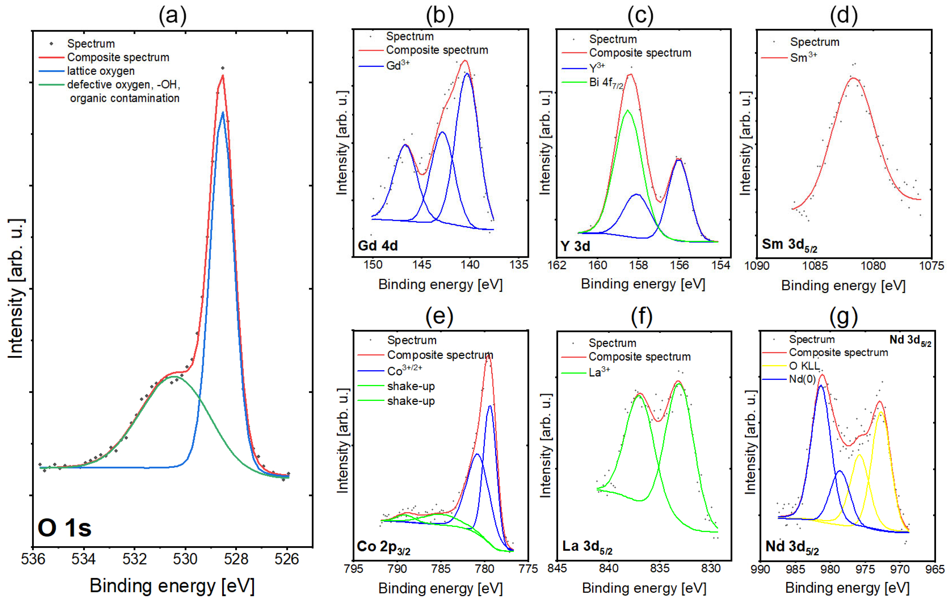
| Element | O | Co | Y | La | Nd | Sm | Gd |
|---|---|---|---|---|---|---|---|
| at-% | |||||||
| Surface | 61.1 ± 6.4 | 17.8 ± 2.1 | 5.3 ± 0.2 | 4.0 ± 0.3 | 3.3 ± 0.3 | 3.4 ± 0.2 | 4.8 ± 0.3 |
| Theoretical | 60.0 | 20.0 | 4.0 | 4.0 | 4.0 | 4.0 | 4.0 |
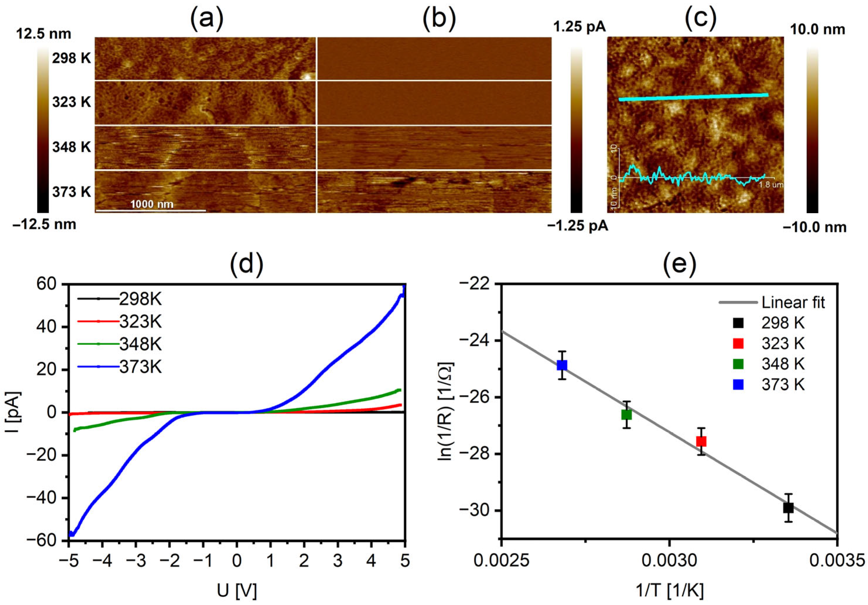
| Method | Energy Gap [eV] | R2 [−] |
|---|---|---|
| AFM U-I | 1.23 ± 0.12 | 0.9810 |
| FPRM | 0.93 ± 0.01 | 0.9995 |
| UV/VIS | 0.88 ± 0.02 | 0.9873 |
| 1.98 ± 0.04 | 0.9934 | |
| 2.66 ± 0.07 | 0.9899 |
Disclaimer/Publisher’s Note: The statements, opinions and data contained in all publications are solely those of the individual author(s) and contributor(s) and not of MDPI and/or the editor(s). MDPI and/or the editor(s) disclaim responsibility for any injury to people or property resulting from any ideas, methods, instructions or products referred to in the content. |
© 2023 by the authors. Licensee MDPI, Basel, Switzerland. This article is an open access article distributed under the terms and conditions of the Creative Commons Attribution (CC BY) license (https://creativecommons.org/licenses/by/4.0/).
Share and Cite
Krawczyk, P.A.; Salamon, W.; Marzec, M.; Szuwarzyński, M.; Pawlak, J.; Kanak, J.; Dziubaniuk, M.; Kubiak, W.W.; Żywczak, A. High-Entropy Perovskite Thin Film in the Gd-Nd-Sm-La-Y-Co System: Deposition, Structure and Optoelectronic Properties. Materials 2023, 16, 4210. https://doi.org/10.3390/ma16124210
Krawczyk PA, Salamon W, Marzec M, Szuwarzyński M, Pawlak J, Kanak J, Dziubaniuk M, Kubiak WW, Żywczak A. High-Entropy Perovskite Thin Film in the Gd-Nd-Sm-La-Y-Co System: Deposition, Structure and Optoelectronic Properties. Materials. 2023; 16(12):4210. https://doi.org/10.3390/ma16124210
Chicago/Turabian StyleKrawczyk, Pawel A., Wojciech Salamon, Mateusz Marzec, Michał Szuwarzyński, Jakub Pawlak, Jarosław Kanak, Małgorzata Dziubaniuk, Władyslaw W. Kubiak, and Antoni Żywczak. 2023. "High-Entropy Perovskite Thin Film in the Gd-Nd-Sm-La-Y-Co System: Deposition, Structure and Optoelectronic Properties" Materials 16, no. 12: 4210. https://doi.org/10.3390/ma16124210