
Effect of Microstructural and Tribological Behaviors of Sputtered Titanium Carbide Thin Film on Copper Substrate
Abstract
:1. Introduction
2. Materials and Methods
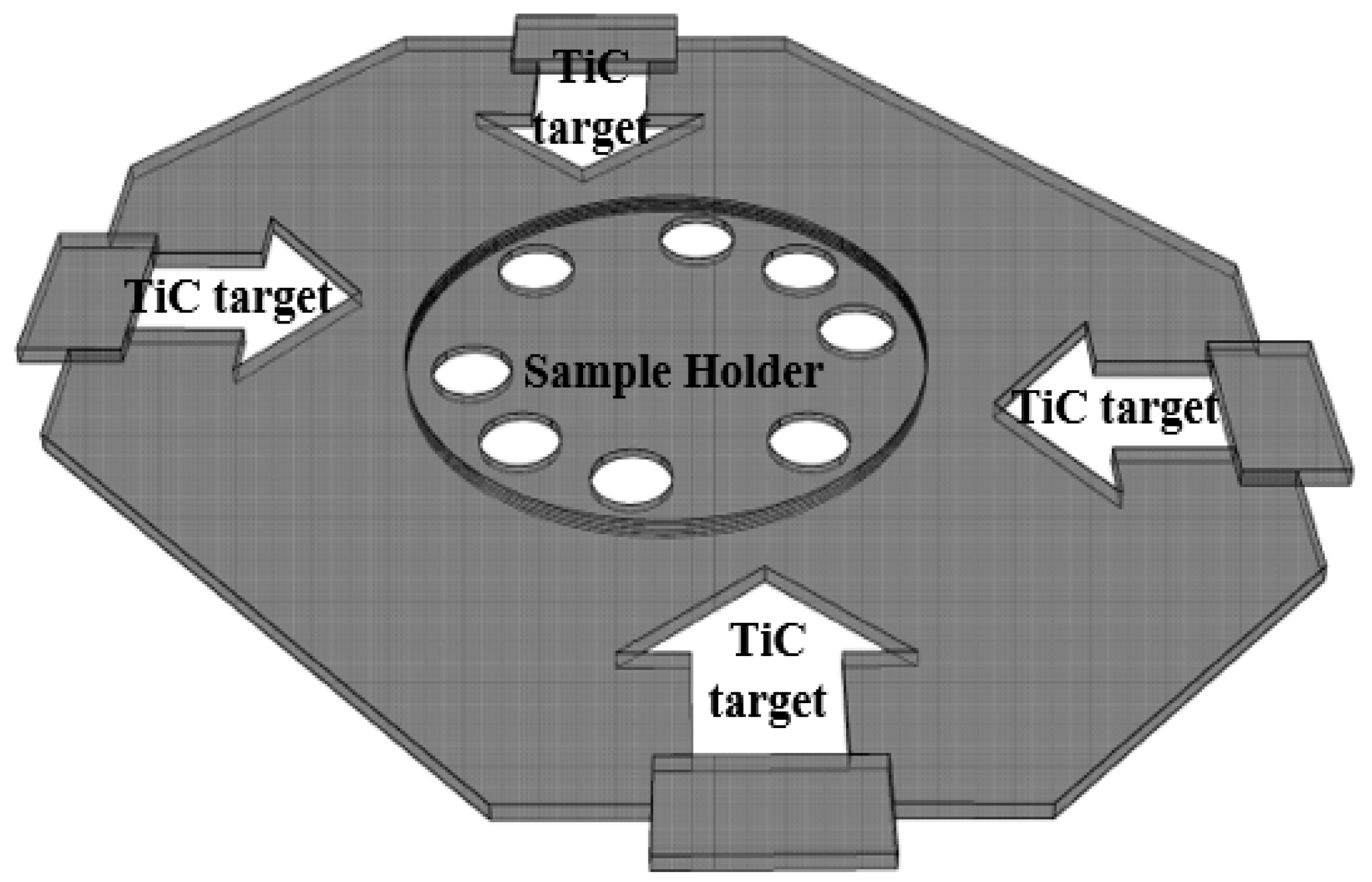
2.1. Thin Films Deposition
2.2. Thin Films’ Characterisation
3. Results and Discussion
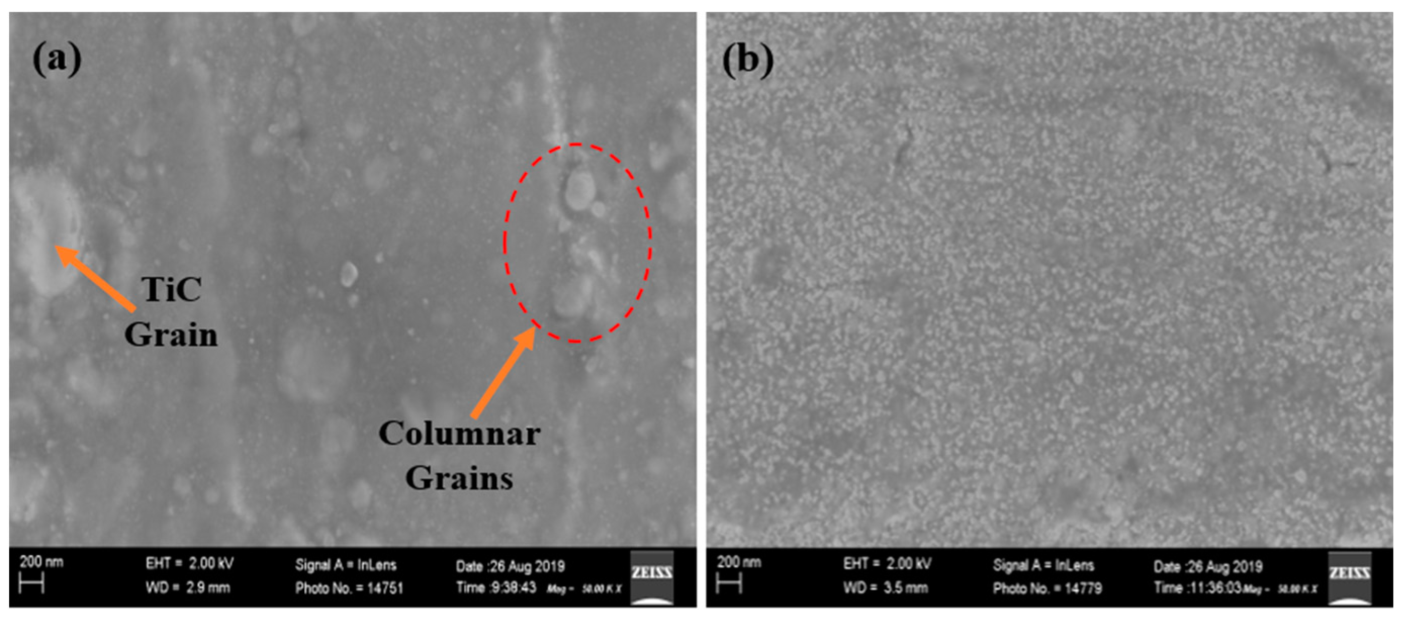
3.1. The SEM Micro-Structural Analysis of the Coated TiC Thin Film
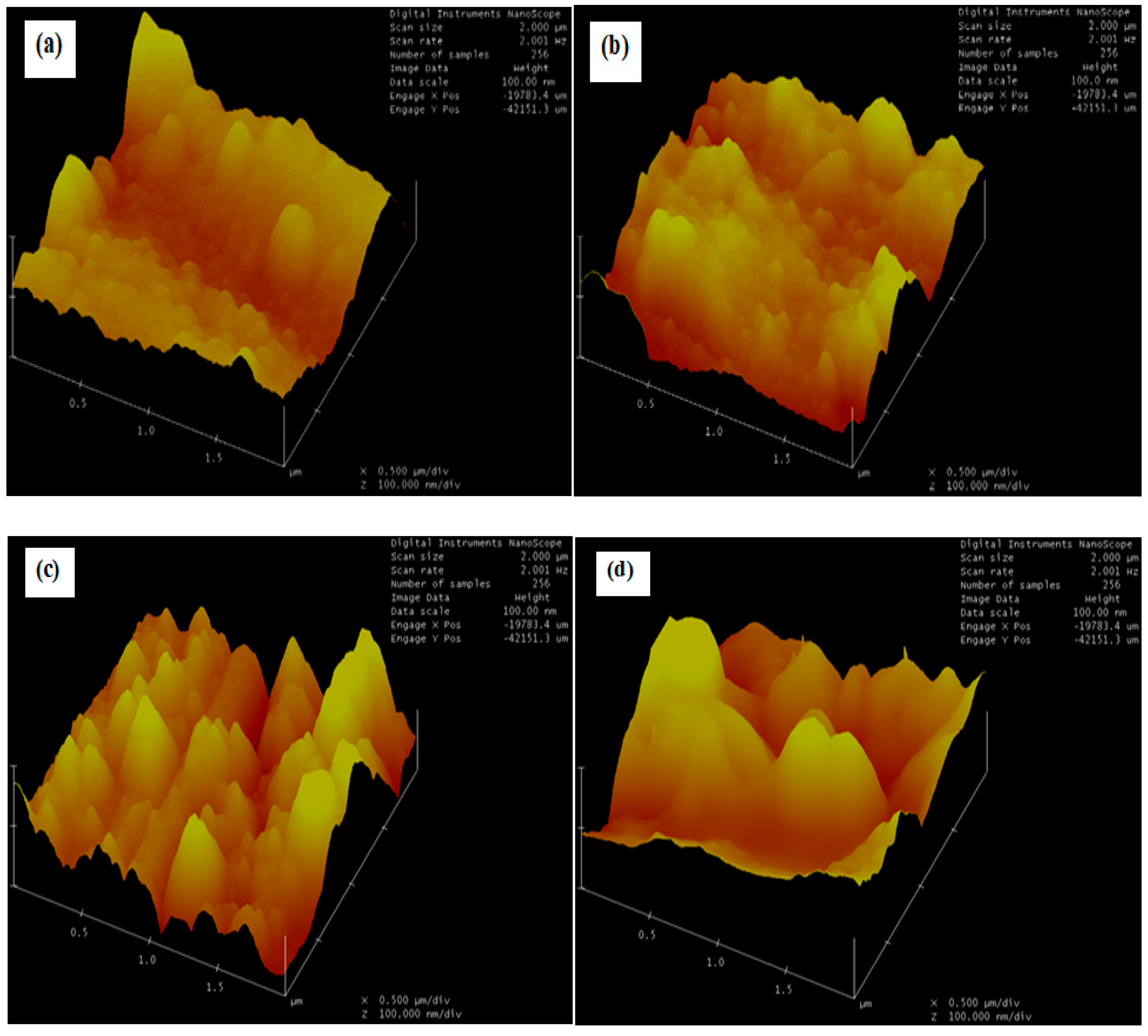
3.2. Atomic Force Microscopy (AFM) Analysis
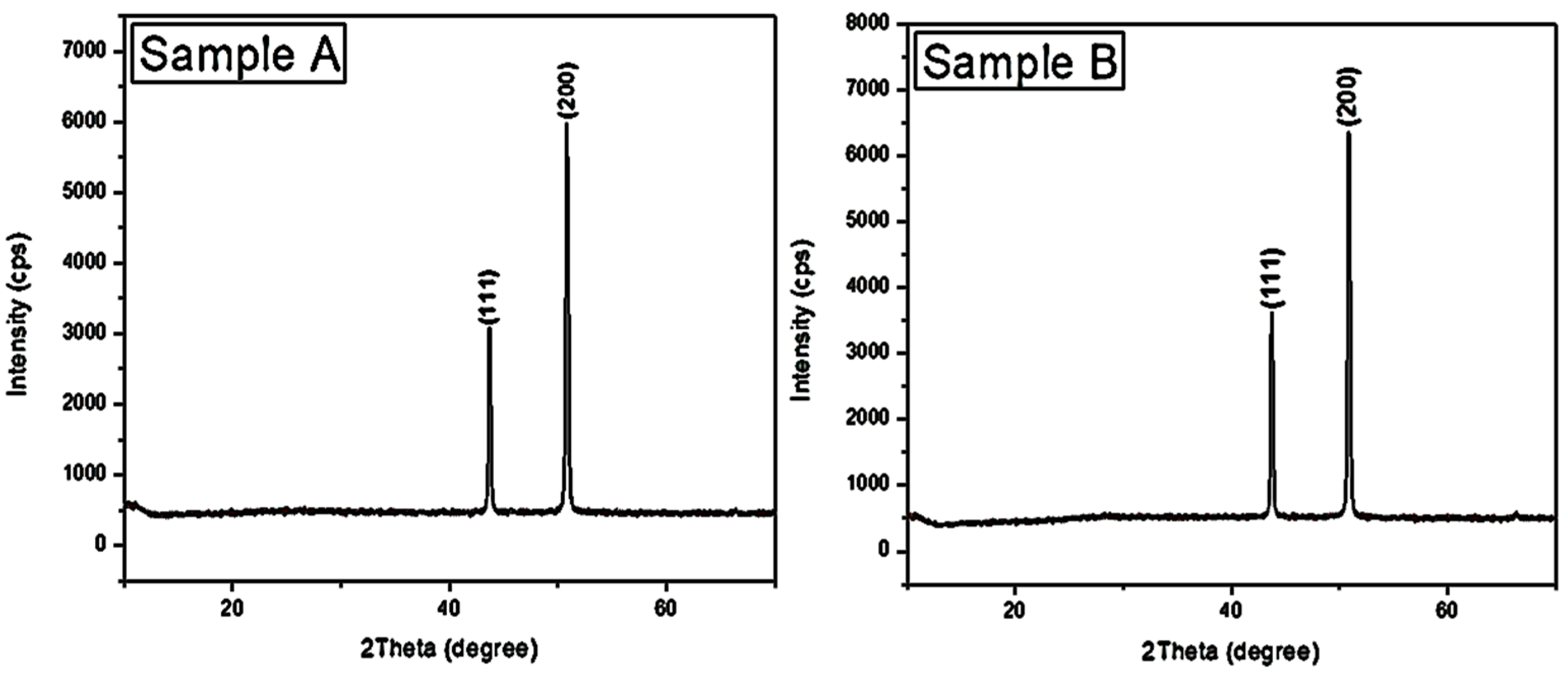
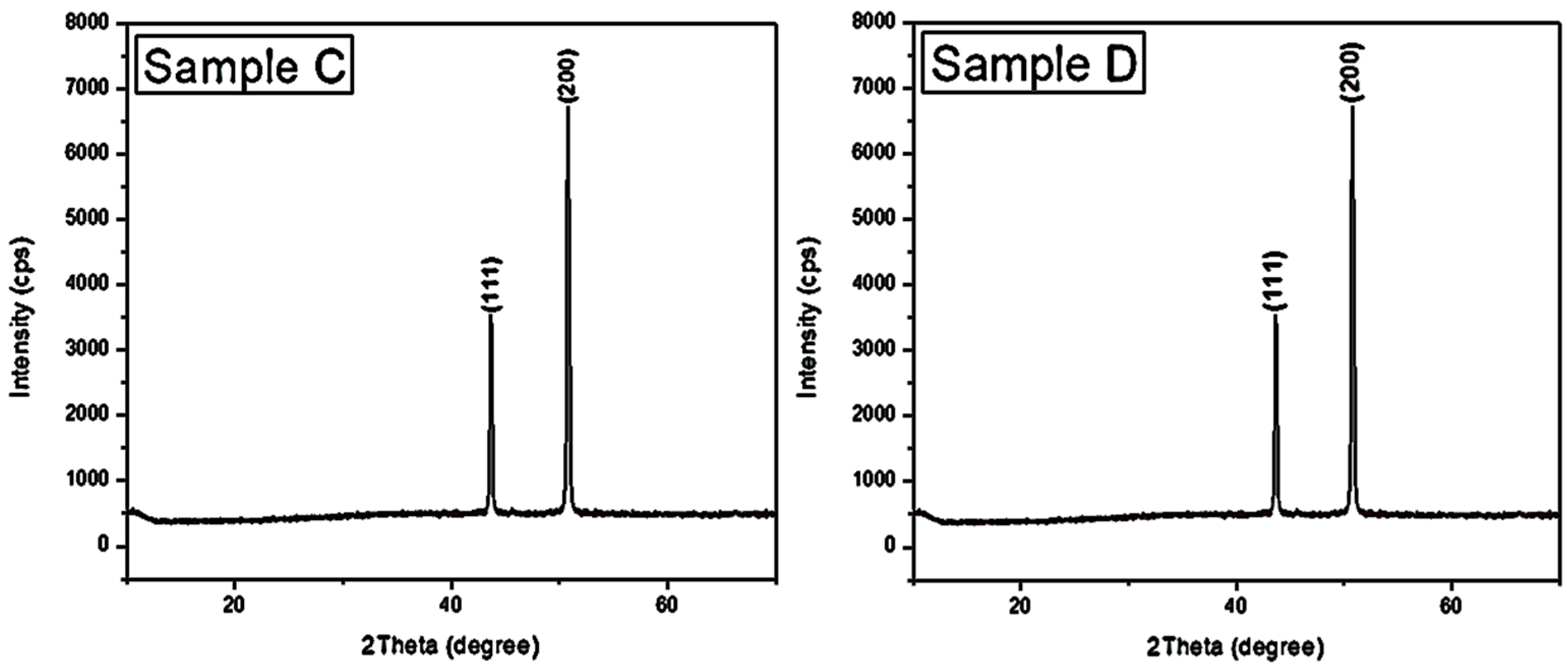
3.3. XRD Analysis of TiC Thin Film Coatings
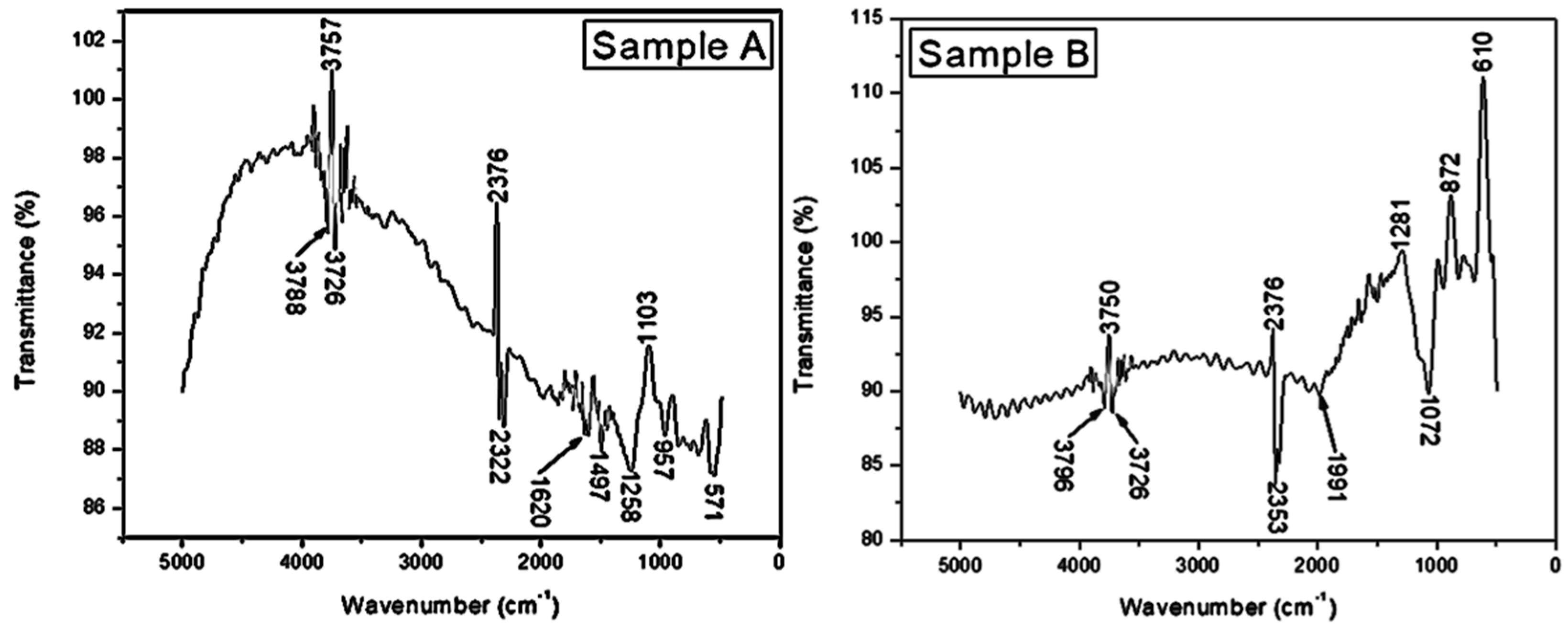
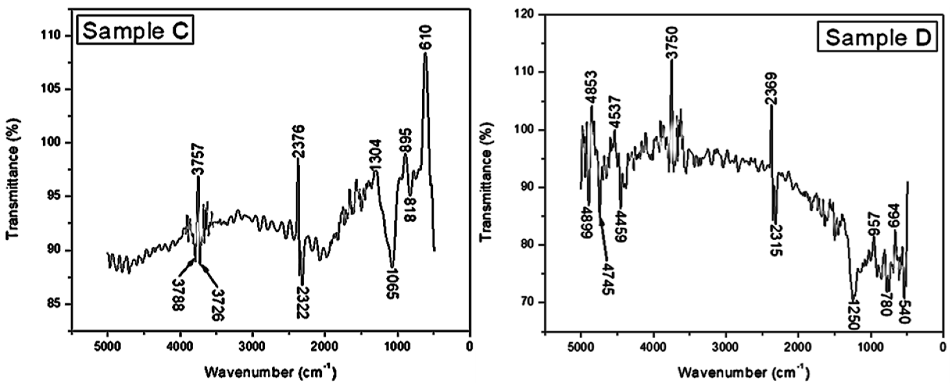
3.4. FTIR Analysis of TiC Thin Film Coatings
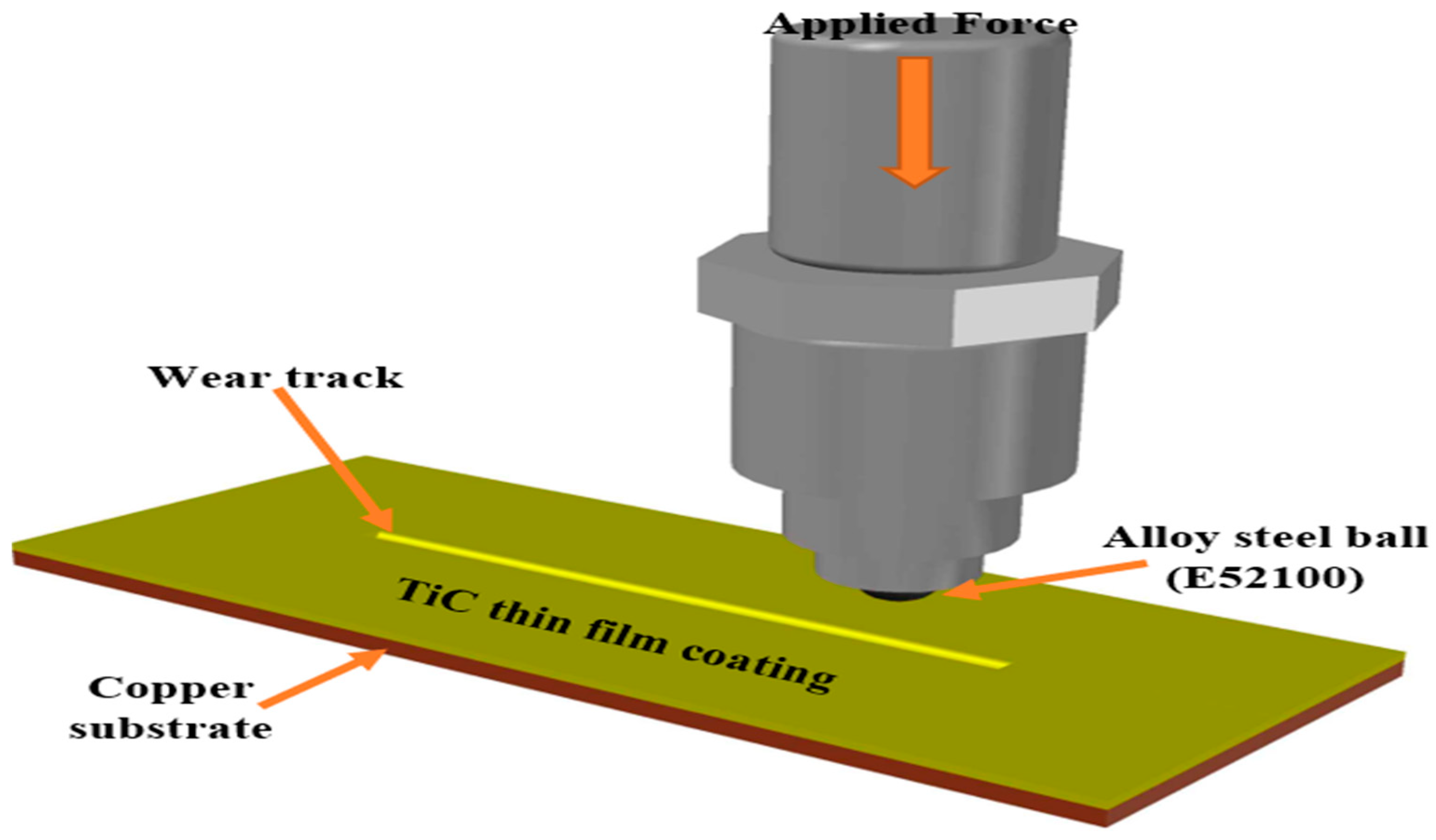
3.5. Tribological Properties and Analysis
3.5.1. Tribological Analysis for TiC Thin Films Deposited on Copper Substrates
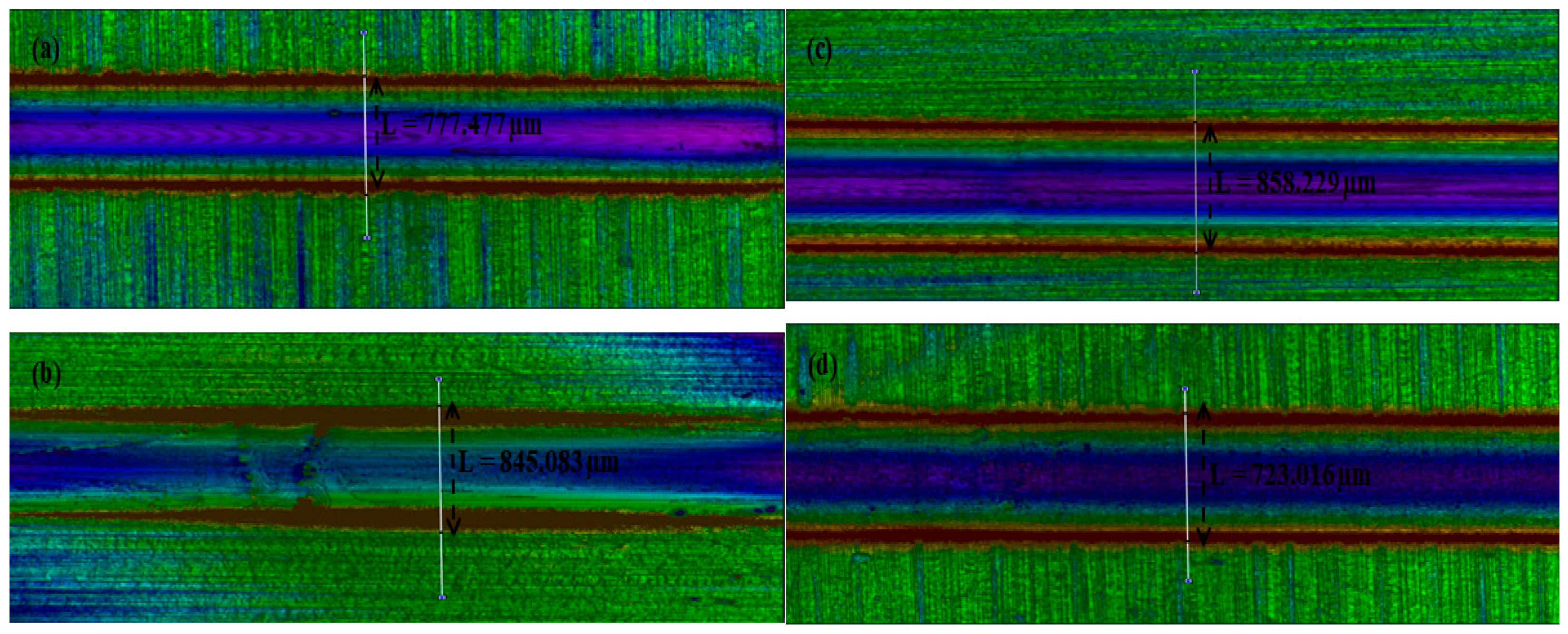
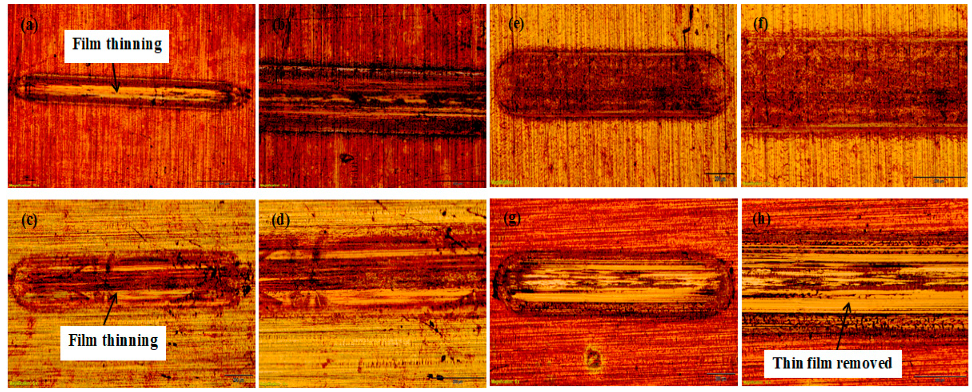
3.5.2. Optical Microscopy Analysis
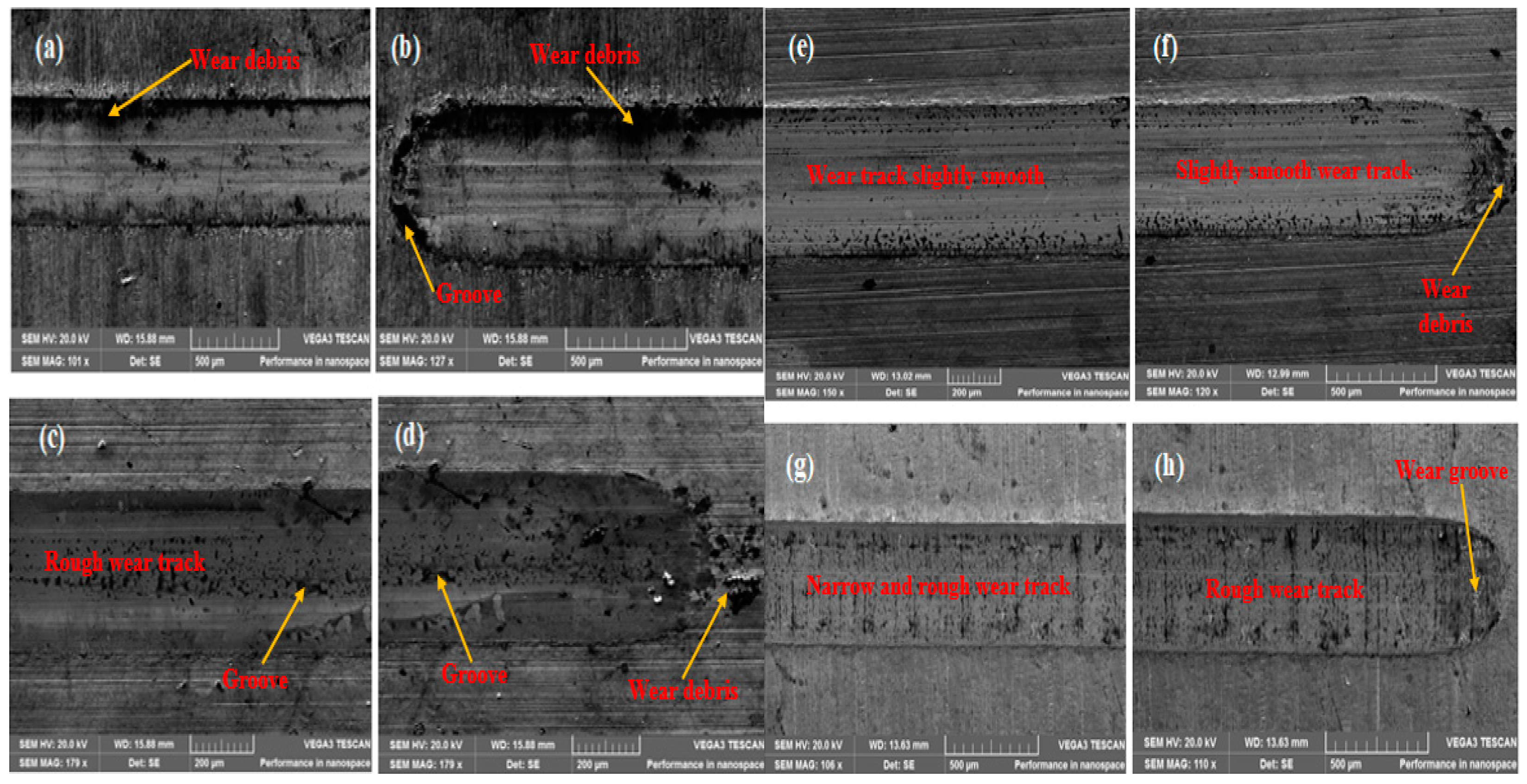
3.5.3. Scanning Electron Microscopy Analysis
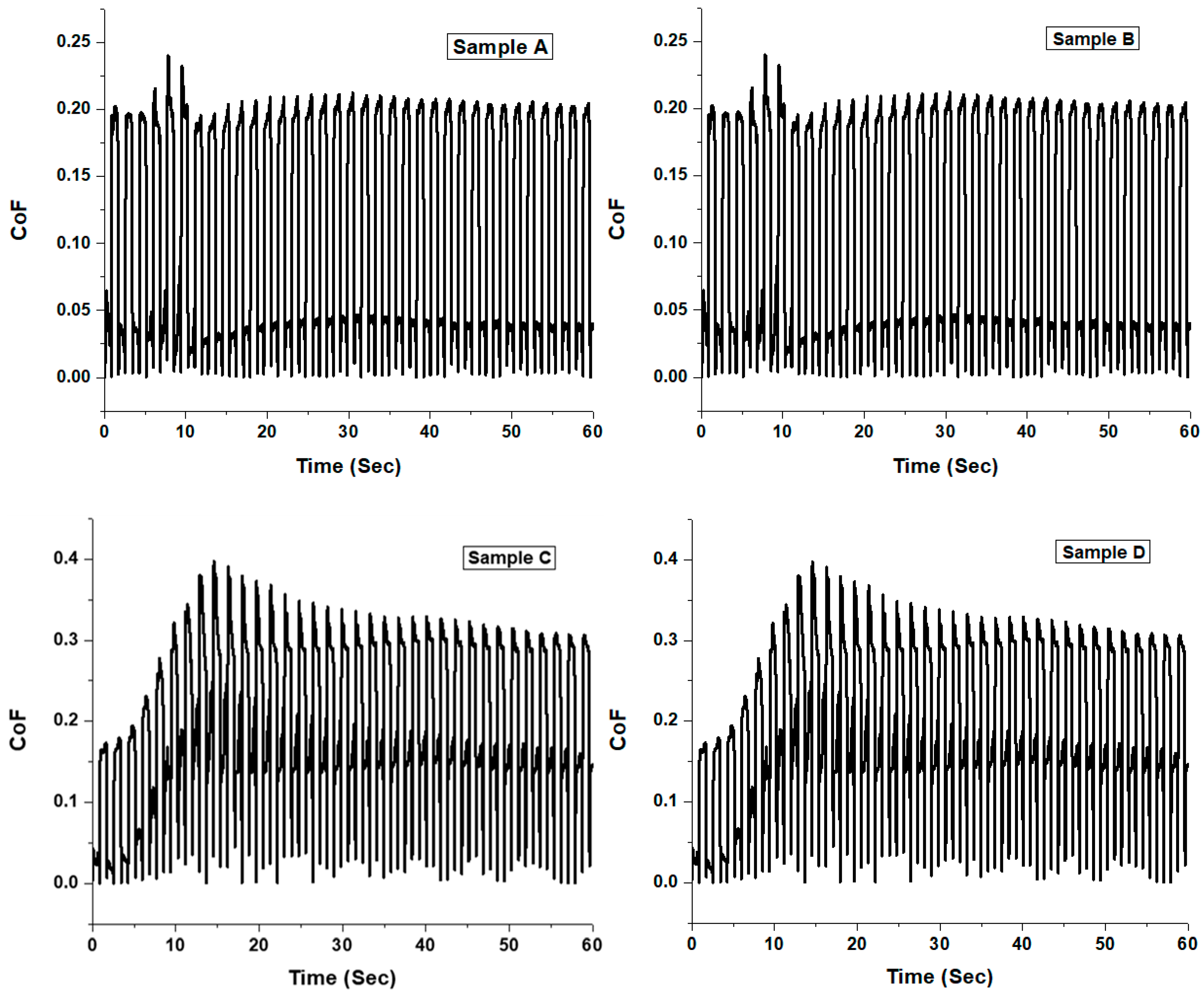
3.5.4. Friction and Sliding Wear Behaviour
4. Conclusions
Author Contributions
Funding
Institutional Review Board Statement
Informed Consent Statement
Data Availability Statement
Acknowledgments
Conflicts of Interest
References
- Ait, Z.D.; Nadia, S.; Noureddine, M.; Abdellatif, Z. Deposition and characterization of titanium carbide thin films by magnetron sputtering using Ti and TiC targets. Appl. Surf. Sci. 2014, 312, 57–62. [Google Scholar]
- Jinga, V.; Mateescu, A.O.; Cristea, D.; Mateescu, G.; Burducea, I.; Ionescu, C.; Cracium, C.L.; Ghiuta, I.; Samoila, C.; Ursutiu, D.; et al. Compositional, morphological and mechanical investigations of monolayer type coatings obtained by standard and reactive magnetron sputtering from Ti, TiB2 and WC. Appl. Surf. Sci. 2015, 358, 579–585. [Google Scholar] [CrossRef]
- Shojiro, M.; Takanori, S.; Manabu, S. Nanomechanical and boundary lubrication properties of titanium carbide and diamond-like carbon nanoperiod multilayer and nanocomposite films. Surf. Coat. Technol. 2013, 221, 124–132. [Google Scholar]
- Ali, R.; Sebastiani, M.; Bemporad, E. Influence of Ti–TiN multilayer PVD–coatings design on residual stresses and adhesion. Mater. Des. 2015, 75, 47–56. [Google Scholar] [CrossRef]
- Yildiz, F.; Yetim, A.F.; Alsaram, A.; Celik, A.; Kaymaz, I.; Efeoglu, I. Palin and fretting behaviour of Ti6Al4V alloy coated with TiAlN thin film. Tribol. Int. 2013, 66, 307–314. [Google Scholar] [CrossRef]
- Wu, J.; Wu, B.H.; Ma, D.L.; Xie, D.; Wu, Y.P.; Chen, C.Z.; Li, Y.T.; Sun, H.; Huang, N.; Leng, Y.X. Effects of magnetic field strength and deposition pressure on the properties of TiN films produced by high power pulsed magnetron sputtering (HPPMS). Surf. Coat. Technol. 2017, 315, 258–267. [Google Scholar] [CrossRef]
- Xianjuan, P.; Lei, S.; Peng, W.; Guangan, Z.; Weimin, L. Influences of bias voltage on mechanical and tribological properties of Ti–Al–C films synthesized by magnetron sputtering. Surf. Coat. Technol. 2009, 203, 1537–1543. [Google Scholar]
- Mohsen, A.; Siti, N.A.; Mohd, F.A.; Zainal, A.A. Structural, surface morphology and optical properties of sputter-coated CaCu3Ti4O12 thin film: Influence of RF magnetron sputtering power. Mater. Sci. Semicond. Process. 2017, 66, 157–161. [Google Scholar]
- Surmenev, R.A.; Surmeneva, M.A.; Grubova, I.Y.; Chernozem, R.V.; Krause, B.; Baumbach, T.; Loza, K.; Epple, M. RF magnetron sputtering of a hydroxyapatite target: A comparison study on polytetrafluorethylene and titanium substrates. Appl. Surf. Sci. 2017, 414, 335–344. [Google Scholar] [CrossRef]
- Sawsen, N.; Nadia, S.; Samira, S.; Mohammed, F.; Mogtaba, M.; Nadia, A.L.; Nouar, T. Properties of TiO2 thin films deposited by rf reactive magnetron sputtering on biased substrates. Appl. Surf. Sci. 2017, 395, 172–179. [Google Scholar]
- Yang, Z.; Hui, W.; Fan, Y.; Zhiyuan, W.; Jingjie, L.; Yutao, G.; Zhennan, F.; Xinzhong, L.; Zhiqiang, Z. Sputtering Power Induced Physical Property Variation of Nickel Oxide Films by Radio Frequency Magnetron Sputtering. Mater. Res. 2018, 21, 1–4. [Google Scholar]
- Muslim, N.; Soon, Y.W.; Lim, C.M.; Voo, N.Y. Influence of sputtering power on properties of titanium thin films deposited by RF magnetron sputtering. ARPN J. Eng. Appl. Sci. 2015, 10, 7184–7189. [Google Scholar]
- Silva, D.L.C.e.; Kassab, L.R.P.; Martinelli, J.R.; dos Santos, A.D.; Riberio, S.J.L.; dos Santos, M.V. Characterization of Thin Carbon Films Produced by the Magnetron Sputtering Technique. Mater. Res. 2016, 19, 669–672. [Google Scholar] [CrossRef]
- Liu, Y.M.; Han, R.Q.; Liu, F.; Pei, Z.L.; Sun, C. Sputtering gas pressure and target power dependence on the microstructure and properties of DC-magnetron sputtered AlB2-type WB2 films. J. Alloys Compd. 2017, 703, 188–197. [Google Scholar] [CrossRef]
- Kirsten, B.; Ralf, P.B.; Thomas, M.; Nazlim, B.; Ricardo, H.B.; Marcel, S.; Jan, T. Continuum and kinetic simulations of the neutral gas flow in an industrial physical vapor-deposition reactor. J. Surf. Coat. Technol. 2013, 237, 176–181. [Google Scholar]
- Xianjuan, P.; Lei, S.; Peng, W.; Yanqiu, X.; Weimin, L. Effects of Al incorporation on the mechanical and tribological properties of Ti-doped a-C:H films deposited by magnetron sputtering. Curr. Appl. Phys. 2011, 11, 771–775. [Google Scholar]
- Huili, W.; Sam, Z.; Yibin, L.; Deen, S. Bias effect on microstructure and mechanical properties of magnetron sputtered nanocrystalline titanium carbide thin films. Thin Solid Films 2008, 516, 5419–5423. [Google Scholar]
- Hamze, F.; Hamid, R.B.; Mohammad, G.M. Chemo-Rheological Behavior of Aqueous Titanium Carbide Suspension and Evaluation of the Gel-coated Green Body Properties. Mater. Res. 2017, 20, 175–182. [Google Scholar]


| Sample | RF Power (W) | Time (h) | Temp (°C) | Argon Gas Flow Rate (sccm) | Grain Size (nm) | RMS (nm) | Roughness, Ra (nm) |
|---|---|---|---|---|---|---|---|
| A | 200 | 3 | 100 | 10 | 54.240 | 29.583 | 24.871 |
| B | 200 | 2 | 80 | 10 | 91.507 | 23.856 | 19.797 |
| C | 200 | 2 | 100 | 10 | 140.440 | 37.029 | 28.361 |
| D | 200 | 3 | 80 | 10 | 83.152 | 42.207 | 33.080 |
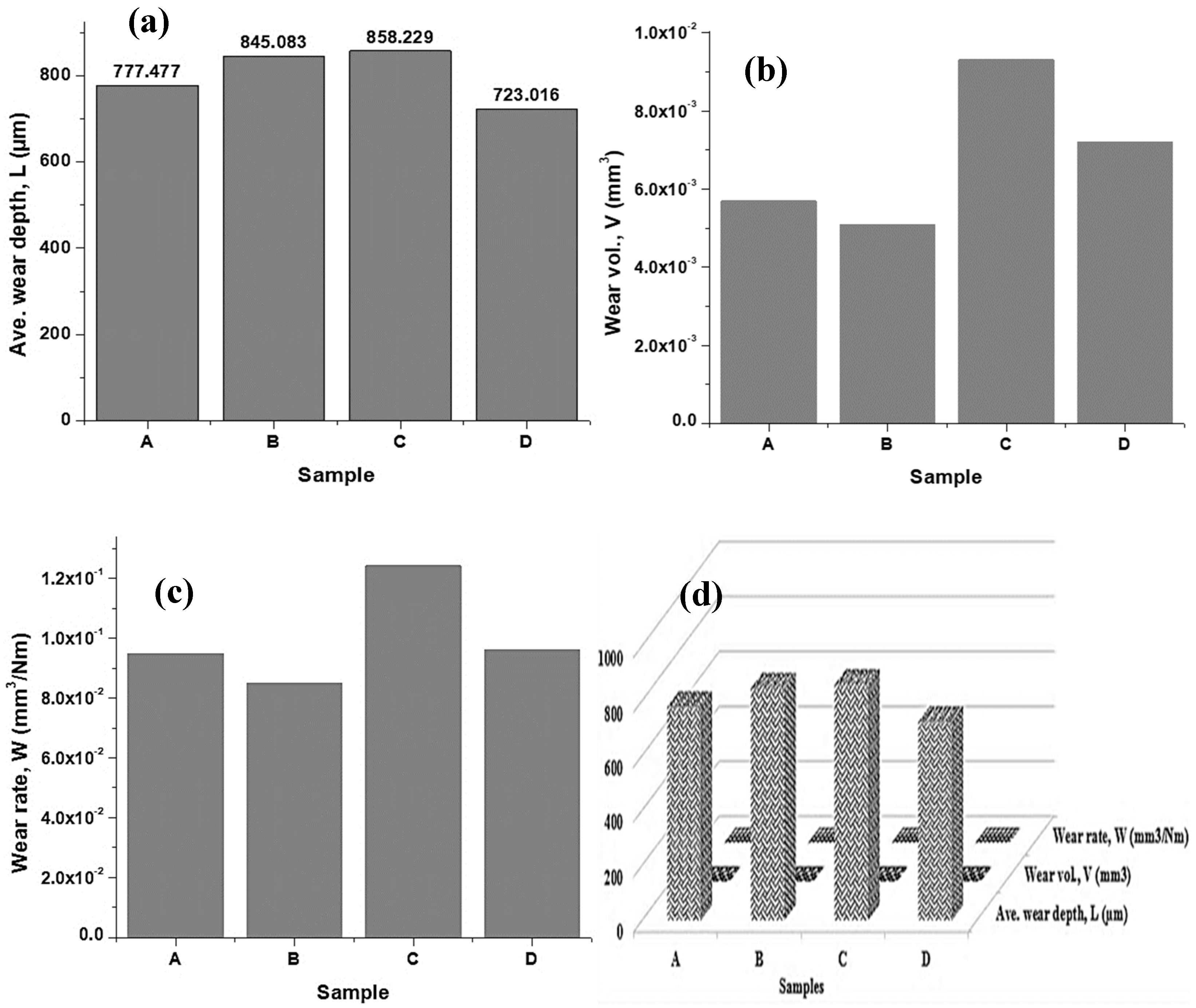
| Sample | Load (N) | L (µm) | ∆X (µm) | ∆H (µm) | Wear vol. (mm3) |
|---|---|---|---|---|---|
| A | 20 | 777.477 | 450.711 | 0.724 | 5.692367exp–3 |
| B | 20 | 845.083 | 490.148 | –1.193 | 5.088833exp–3 |
| C | 25 | 858.229 | 507.050 | 0.434 | 9.310995exp–3 |
| D | 25 | 723.016 | 482.636 | 0.143 | 7.195599exp–3 |
| Sample | Ave. Wear Depth, L (µm) | Wear vol., V (mm3) | Wear Rate, W (mm3/Nm) |
|---|---|---|---|
| A | 777.477 | 5.692367exp–3 | 0.094873 |
| B | 845.083 | 5.088833exp–3 | 0.084818 |
| C | 858.229 | 9.310995exp–3 | 0.124147 |
| D | 723.016 | 7.195599exp–3 | 0.095941 |
Disclaimer/Publisher’s Note: The statements, opinions and data contained in all publications are solely those of the individual author(s) and contributor(s) and not of MDPI and/or the editor(s). MDPI and/or the editor(s) disclaim responsibility for any injury to people or property resulting from any ideas, methods, instructions or products referred to in the content. |
© 2022 by the authors. Licensee MDPI, Basel, Switzerland. This article is an open access article distributed under the terms and conditions of the Creative Commons Attribution (CC BY) license (https://creativecommons.org/licenses/by/4.0/).
Share and Cite
Ogunlana, M.O.; Muchie, M.; Oladijo, O.P.; Erinosho, M. Effect of Microstructural and Tribological Behaviors of Sputtered Titanium Carbide Thin Film on Copper Substrate. Materials 2023, 16, 174. https://doi.org/10.3390/ma16010174
Ogunlana MO, Muchie M, Oladijo OP, Erinosho M. Effect of Microstructural and Tribological Behaviors of Sputtered Titanium Carbide Thin Film on Copper Substrate. Materials. 2023; 16(1):174. https://doi.org/10.3390/ma16010174
Chicago/Turabian StyleOgunlana, Musibau Olalekan, Mammo Muchie, Oluseyi Philip Oladijo, and Mutiu Erinosho. 2023. "Effect of Microstructural and Tribological Behaviors of Sputtered Titanium Carbide Thin Film on Copper Substrate" Materials 16, no. 1: 174. https://doi.org/10.3390/ma16010174