
Manufacturing of a Magnetic Composite Flexible Filament and Optimization of a 3D Printed Wideband Electromagnetic Multilayer Absorber in X-Ku Frequency Bands

 , ,
, ,
Abstract
:1. Introduction
2. Materials and Methods
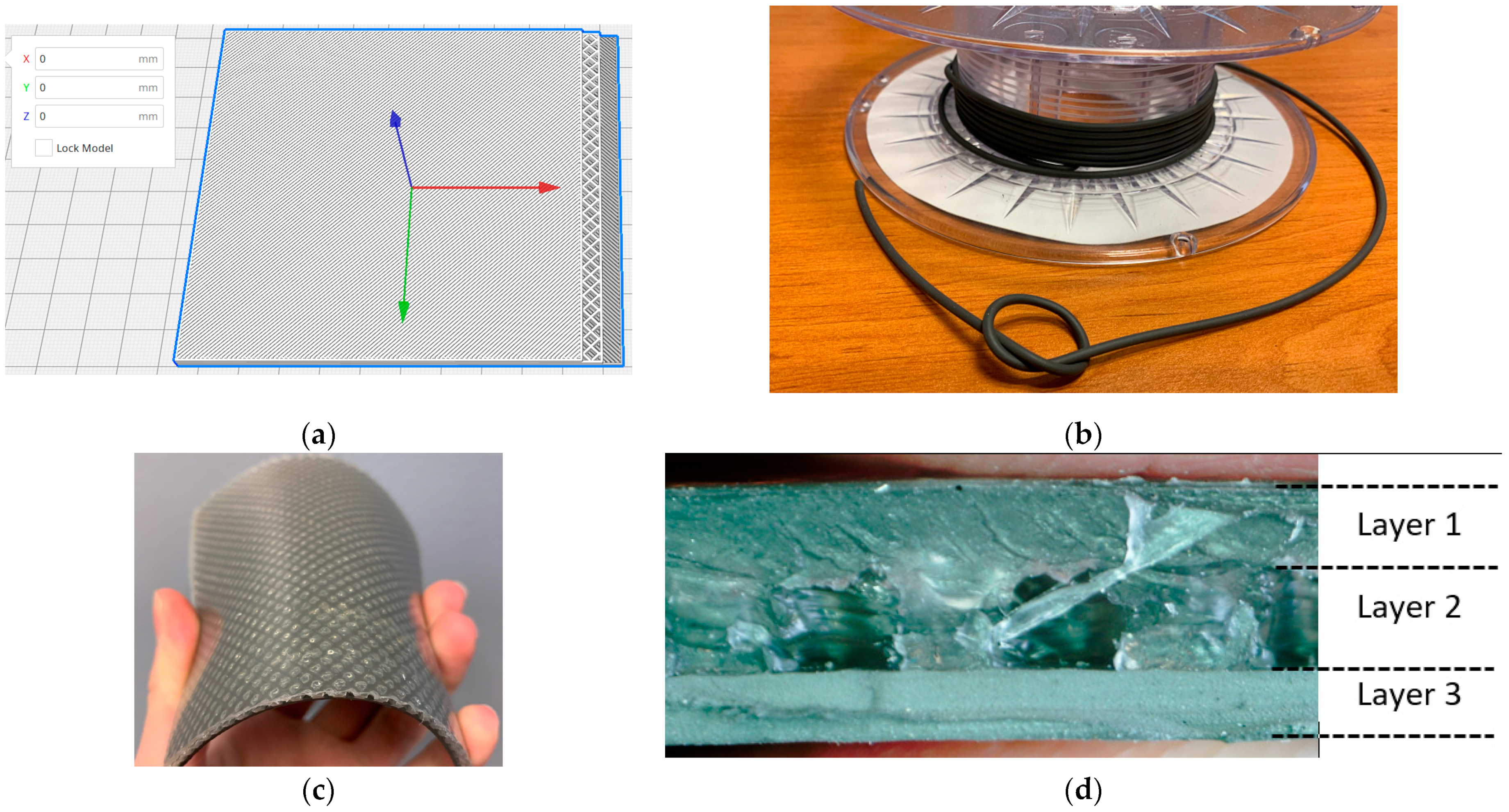
2.1. Materials and Filament Preparation
2.2. Characterization Techniques
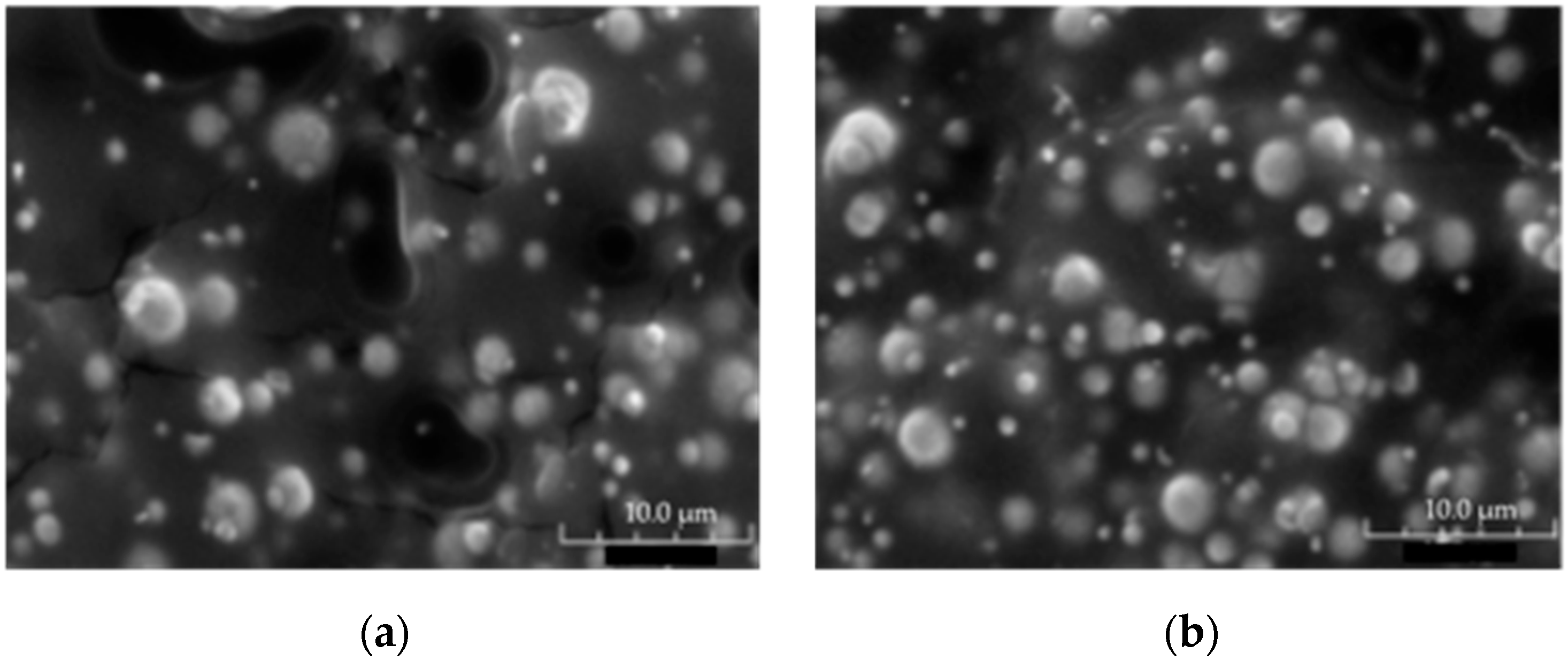
2.2.1. Microstructure Observation
2.2.2. Electromagnetic Characterization
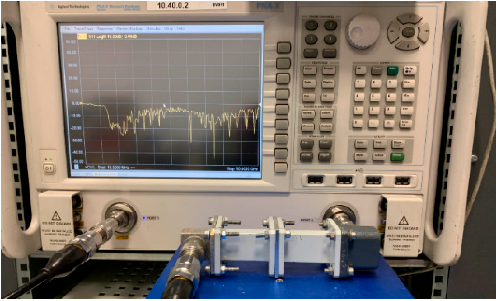
2.2.3. Measurement of the Reflectivity of the Absorber
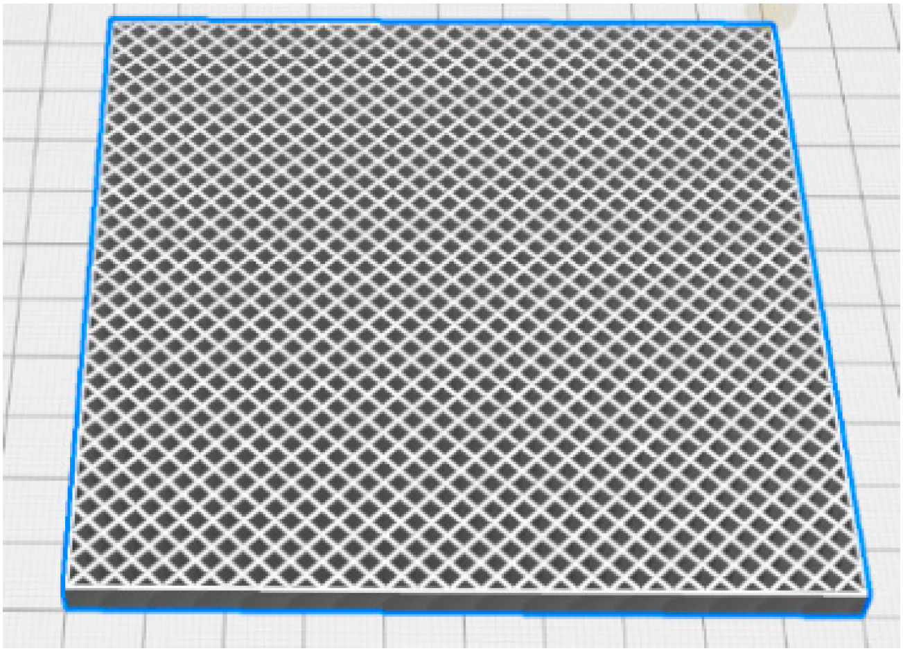
2.3. Structure Optimization
- The lossless filament when fully dense;
- The magnetic loaded filament when fully dense;
- The lossless filament with the “Grid” porous pattern.
3. Results
3.1. Microstructure Observation
3.2. Microwave Characterization
3.3. Structure Optimization
3.4. 3D Printing
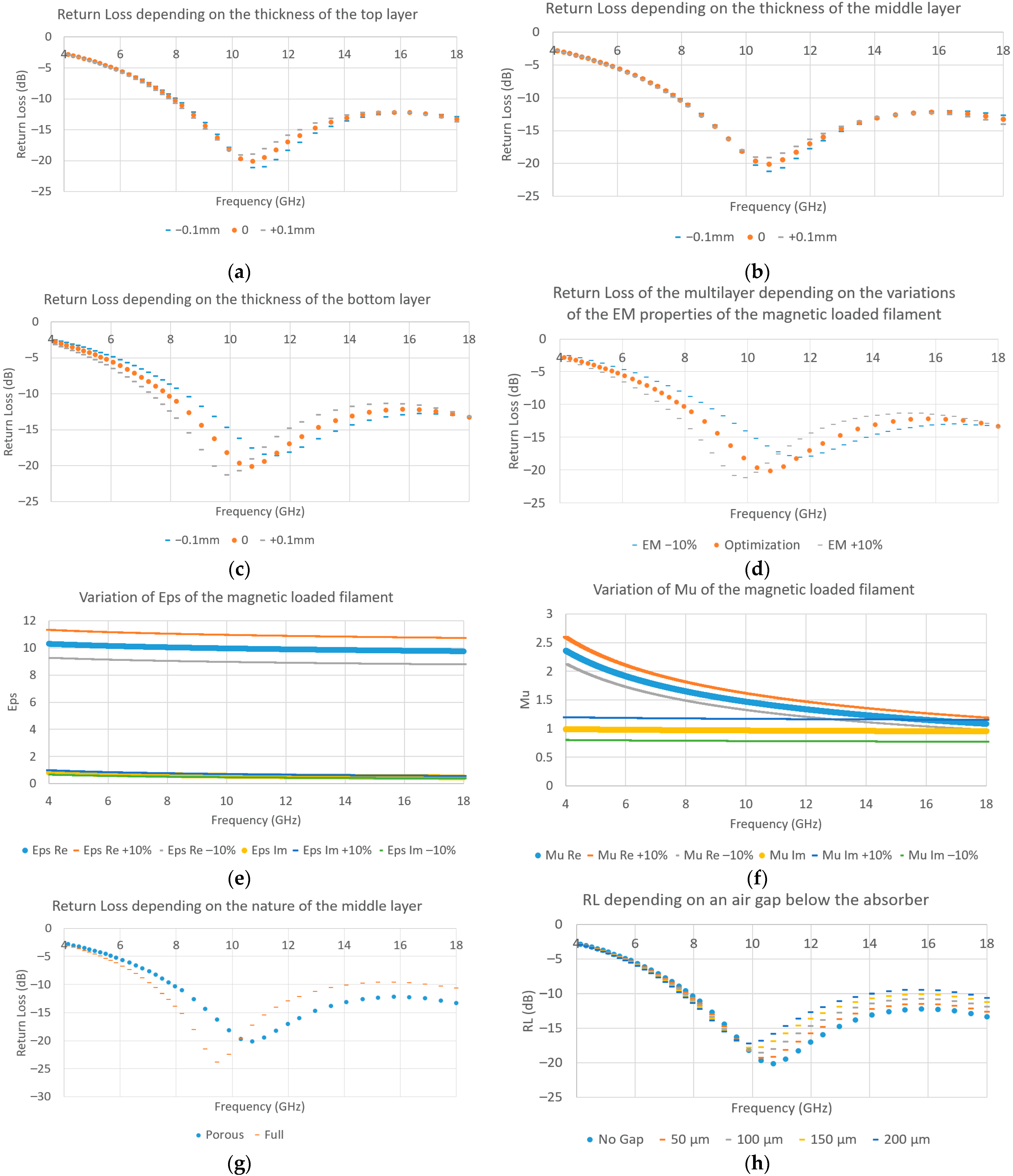
4. Discussion
5. Conclusions
Author Contributions
Funding
Institutional Review Board Statement
Informed Consent Statement
Data Availability Statement
Conflicts of Interest
References
- Knott, E.F.; Schaeffer, J.F.; Tulley, M.T. Radar Cross Section; SciTech Publishing: New York, NY, USA, 2004. [Google Scholar]
- Redl, R. Electromagnetic Environmental Impact of Power Electronics Equipment. Proc. IEEE 2001, 89, 926–938. [Google Scholar] [CrossRef]
- Arbaoui, Y.; Laur, V.; Maalouf, A.; Queffelec, P. 3D printing for microwave: Materials characterization and application in the field of absorbers. In Proceedings of the 2015 IEEE MTT-S International Microwave Symposium IEEE, Phoenix, AZ, USA, 17–22 May 2015; pp. 1–3. [Google Scholar]
- Holloway, C.L.; Kuester, E.F. A low-frequency model for wedge or pyramid absorber arrays-II: Computed and measured results. IEEE Trans. Electromagn. Compat. 1994, 36, 307–313. [Google Scholar] [CrossRef]
- Chen, M.; Zhu, Y.; Pan, Y.; Kou, H.; Xu, H.; Guo, J. Gradient multilayer structural design of CNTs/SiO2 composites for improving microwave absorbing properties. Mater. Des. 2011, 32, 3013–3016. [Google Scholar] [CrossRef]
- Costa, F.; Monorchio, A.; Manara, G. Theory, design and perspectives of electromagnetic wave absorbers. IEEE Electromagn. Compat. Mag. 2016, 5, 67–74. [Google Scholar] [CrossRef] [Green Version]
- Chew, W.C. Waves and Fields in Inhomogeneous Media; IEEE Press: New York, NY, USA, 1995. [Google Scholar]
- Michielssen, E.; Sajer, J.M.; Ranjithan, S.; Mittra, R. Design of lightweight, broad-band microwave absorbers using genetic algorithms. IEEE Trans. Microw. Theory Tech. 1993, 41, 1024–1031. [Google Scholar] [CrossRef]
- Roy, S.; Roy, S.D.; Tewary, J.; Mahanti, A.; Mahanti, G.K. Particle swarm optimization for optimal design of broadband multilayer microwave absorber for wide angle of incidence. Prog. Electromagn. Res. 2015, 62, 121–135. [Google Scholar] [CrossRef] [Green Version]
- Chevalier, A.; Laur, V. Composites-based microwave absorbers: Toward a unified model. In Proceedings of the 2017 IEEE MTT-S International Microwave Symposium (IMS), Honololu, HI, USA, 4–9 June 2017; pp. 1804–1807. [Google Scholar]
- Li, L.; Lv, Z. Ultra-wideband polarization-insensitive and wide-angle thin absorber based on resistive metasurfaces with three resonant modes. J. Appl. Phys. 2017, 122, 055104. [Google Scholar] [CrossRef]
- Pan, K.; Leng, T.; Song, J.; Ji, C.; Zhang, J.; Li, J.; Novoselov, K.S.; Hu, Z. Controlled reduction of graphene oxide laminate and its applications for ultra-wideband microwave absorption. Carbon 2020, 160, 307–316. [Google Scholar] [CrossRef]
- Kim, Y.; Park, P.; Jo, J.; Lee, J.; Jeong, L.; Shin, J.; Lee, J.-H.; Lee, H.-J. Ultrawideband electromagnetic metamaterial absorber utilizing coherent absorptions and surface plasmon polaritons based on double layer carbon metapatterns. Sci. Rep. 2021, 11, 23045. [Google Scholar] [CrossRef] [PubMed]
- Yin, L.; Tian, X.; Shang, Z.; Li, D. Ultra-broadband metamaterial absorber with graphene composites fabricated by 3D printing. Mater. Lett. 2019, 239, 132–135. [Google Scholar] [CrossRef]
- Ren, J.; Yin, J.Y. 3D-Printed Low-Cost Dielectric-Resonator-Based Ultra-Broadband Microwave Absorber Using Carbon-Loaded Acrylonitrile Butadiene Styrene Polymer. Materials 2018, 11, 1249. [Google Scholar] [CrossRef] [PubMed] [Green Version]
- Ghosh, S.; Lim, S. Perforated lightweight broadband metamaterial absorber based on 3-D printed honeycomb. IEEE Antennas Wirel. Propag. Lett. 2018, 17, 2379–2383. [Google Scholar] [CrossRef]
- Abshinova, M.A.; Lopatin, A.V.; Kazantseva, N.E.; Vilčáková, J.; Sáha, P. Correlation between the microstructure and the electromagnetic properties of carbonyl iron filled polymer composites. Compos. Part A Appl. Sci. Manuf. 2007, 38, 2471–2485. [Google Scholar] [CrossRef]
- Baker-Jarvis, J.R.; Janezic, M.D.; Riddle, B.F.; Johnk, R.T.; Holloway, C.L.; Geyer, R.G.; Grosvenor, C.A. Measuring the Permittivity and Permeability of Lossy Materials; Technical Note (NIST TN)-1536; NIST: Gaithersburg, MD, USA, 2005. [Google Scholar]
- Dib, N.; Asi, M.; Sabbah, A.I. On the optimal design of multilayer microwave absorbers. Prog. Electromagn. Res. C 2010, 13, 171–185. [Google Scholar] [CrossRef] [Green Version]
- Find Minimum of Function Using Genetic Algorithm—MATLAB ga. Available online: https://www.mathworks.com/help/gads/ga.html (accessed on 11 April 2022).
- Smoluchowski, M.v. Versuch einer mathematischen Theorie der Koagulationskinetik kolloider Lösungen. Z. Phys. Chem. 1918, 92, 129–168. [Google Scholar] [CrossRef] [Green Version]
- Chesters, A. Modelling of coalescence processes in fluid-liquid dispersions: A review of current understanding. Chem. Eng. Res. Des. 1991, 69, 259–270. [Google Scholar]


| I Simultaneous Melt Mixing Using a Twin-Screw Extruder | II Pellets Processing | III Filament Processing | ||
|---|---|---|---|---|
| Laboratory scale | Twin-screw extrusion T = 160 °C, N = 150 rpm | (1) Nitrogen cooling (2) Pelletizing | (1) Extrusion (conveying) T = 200 °C, N = 20 rpm (2) Coiling v = 1.6 m/min | (3) Air cooling φ = 2.85 mm ± 500 µm |
| Semi-industrial scale | (3) Water cooling φ = 2.85 mm ± 200 µm | |||
| Industrial-scale | (3) Water cooling φ = 2.85 mm ± 50 µm | |||
| N° Layer | Composition | Thickness (mm) |
|---|---|---|
| 1 | Non-loaded | 0.3 |
| 2 | Magnetic loaded | 0.1 |
| 3 | Non-loaded | 0.2 |
| 4 | Non-loaded with porosity | 0.2 |
| 5 | Non-loaded | 0.1 |
| 6 | Non-loaded with porosity | 0.7 |
| 7 | Non-loaded | 0.2 |
| 8 | Non-loaded with porosity | 0.2 |
| 9 | Non-loaded | 0.1 |
| 10 | Non-loaded with porosity | 0.1 |
| 11 | Non-loaded | 0.1 |
| 12 | Non-loaded with porosity | 0.1 |
| 13 | Non-loaded | 0.2 |
| 14 | Non-loaded with porosity | 0.2 |
| 15 | Magnetic loaded | 1.2 |
| N° Layer | Composition | Thickness (mm) |
|---|---|---|
| 1 | Non-loaded | 1.3 |
| 2 | Non-loaded with porosity | 1.6 |
| 3 | Magnetic loaded | 1.2 |
| N° Layer | Optimized Thickness (mm) | Measured Thickness (mm) |
|---|---|---|
| 1 | 1.3 | 1.25 |
| 2 | 1.6 | 1.81 |
| 3 | 1.2 | 1.05 |
Publisher’s Note: MDPI stays neutral with regard to jurisdictional claims in published maps and institutional affiliations. |
© 2022 by the authors. Licensee MDPI, Basel, Switzerland. This article is an open access article distributed under the terms and conditions of the Creative Commons Attribution (CC BY) license (https://creativecommons.org/licenses/by/4.0/).
Share and Cite
Vong, C.; Chevalier, A.; Maalouf, A.; Ville, J.; Rosnarho, J.-F.; Laur, V. Manufacturing of a Magnetic Composite Flexible Filament and Optimization of a 3D Printed Wideband Electromagnetic Multilayer Absorber in X-Ku Frequency Bands. Materials 2022, 15, 3320. https://doi.org/10.3390/ma15093320
Vong C, Chevalier A, Maalouf A, Ville J, Rosnarho J-F, Laur V. Manufacturing of a Magnetic Composite Flexible Filament and Optimization of a 3D Printed Wideband Electromagnetic Multilayer Absorber in X-Ku Frequency Bands. Materials. 2022; 15(9):3320. https://doi.org/10.3390/ma15093320
Chicago/Turabian StyleVong, Christophe, Alexis Chevalier, Azar Maalouf, Julien Ville, Jean-François Rosnarho, and Vincent Laur. 2022. "Manufacturing of a Magnetic Composite Flexible Filament and Optimization of a 3D Printed Wideband Electromagnetic Multilayer Absorber in X-Ku Frequency Bands" Materials 15, no. 9: 3320. https://doi.org/10.3390/ma15093320