Review

Tin Diselenide (SnSe2) Van der Waals Semiconductor: Surface Chemical Reactivity, Ambient Stability, Chemical and Optical Sensors

1
Department of Physical and Chemical Sciences, University of L’Aquila, via Vetoio, 67100 L’Aquila, Italy
2
Departamento de Física de la Materia Condensada, Universidad Autónoma de Madrid, 28049 Madrid, Spain
3
Instituto “Nicolás Cabrera”, Universidad Autónoma de Madrid, 28049 Madrid, Spain
4
Condensed Matter Physics Center (IFIMAC), 28049 Madrid, Spain
5
Department of Physics, National Cheng Kung University, 1 Ta-Hsueh Road, Tainan 70101, Taiwan
6
Taiwan Consortium of Emergent Crystalline Materials, Ministry of Science and Technology, Taipei 10601, Taiwan
7
CNR-SPIN UoS L’Aquila, Via Vetoio, 67100 L’Aquila, Italy
8
College of Science, Institute of Materials Physics and Chemistry, Nanjing Forestry University, Nanjing 210037, China
9
Theoretical Physics and Applied Mathematics Department, Ural Federal University, Mira Street 19, 620002 Ekaterinburg, Russia
10
CNR-IMM Istituto per la Microelettronica e Microsistemi, VIII strada 5, I-95121 Catania, Italy
*
Authors to whom correspondence should be addressed.
Materials 2022, 15(3), 1154; https://doi.org/10.3390/ma15031154
Submission received: 8 December 2021 / Revised: 25 January 2022 / Accepted: 26 January 2022 / Published: 2 February 2022
(This article belongs to the Topic Multiple Application for Novel and Advanced Materials)

Abstract

:
Tin diselenide (SnSe2) is a layered semiconductor with broad application capabilities in the fields of energy storage, photocatalysis, and photodetection. Here, we correlate the physicochemical properties of this van der Waals semiconductor to sensing applications for detecting chemical species (chemosensors) and millimeter waves (terahertz photodetectors) by combining experiments of high-resolution electron energy loss spectroscopy and X-ray photoelectron spectroscopy with density functional theory. The response of the pristine, defective, and oxidized SnSe2 surface towards H2, H2O, H2S, NH3, and NO2 analytes was investigated. Furthermore, the effects of the thickness were assessed for monolayer, bilayer, and bulk samples of SnSe2. The formation of a sub-nanometric SnO2 skin over the SnSe2 surface (self-assembled SnO2/SnSe2 heterostructure) corresponds to a strong adsorption of all analytes. The formation of non-covalent bonds between SnO2 and analytes corresponds to an increase of the magnitude of the transferred charge. The theoretical model nicely fits experimental data on gas response to analytes, validating the SnO2/SnSe2 heterostructure as a suitable playground for sensing of noxious gases, with sensitivities of 0.43, 2.13, 0.11, 1.06 [ppm]−1 for H2, H2S, NH3, and NO2, respectively. The corresponding limit of detection is 5 ppm, 10 ppb, 250 ppb, and 400 ppb for H2, H2S, NH3, and NO2, respectively. Furthermore, SnSe2-based sensors are also suitable for fast large-area imaging applications at room temperature for millimeter waves in the THz range.

1. Introduction

Following the advent of graphene [1,2,3,4], the scientific community has begun to consider layered semiconductors for their potential application to complement those of graphene [5,6,7,8,9], thus generating promising new technologies in various technological areas [10,11,12,13,14,15,16]. The class of materials of ‘van der Waals semiconductors’ is characterized by weak van der Waals bonds between the layers that allow their exfoliation by mechanical [17,18] and liquid-phase [19,20,21] exfoliation.
The most common van der Waals semiconductors have shown limitations, which compromise their technological development. For example, MoS2 and WS2 have a poor electric mobility of a few tens of cm2V−1s−1 at T = 300 K [22]; black phosphorus is instable in air and undergoes a rapid surface oxidation which degrades the morphology of the surface [23]; GaSe exhibits instability upon both laser and air exposure [24,25]; and PdSe2 [26,27] has a limited commercial potential, due to the constantly growing price of Pd (2000–2400 $/oz), nearly doubled in 2019–2021.
Tin diselenide (SnSe2) is a layered semiconductor constituted by Earth-abundant and cheap elements [28], which crystallizes in a layered CdI2–type structure with hexagonally packed layers of Sn atoms sandwiched between two layers of Se anions (Figure 1a,b) [29,30,31]. Differently from MoS2 and WS2, SnSe2 has a high intrinsic electron mobility at T = 300 K (462.6 cm2V−1s−1) and ultralow thermal conductivity (3.82 W m−1 K−1) [32]. Furthermore, SnSe2 exhibits pressure-induced periodic lattice distortion and, moreover its atomic structure can reversibly change from amorphous to crystalline upon laser heating, being a phase change memory material. Owing to these peculiarities, SnSe2 has high application capabilities in several fields, including superconductivity [33,34], Li [29,35] and Na [29,36] ion batteries, photodetection [37], photocatalysis [38,39], saturable absorbers for eye-safe lasers [40], and thermoelectricity [41,42].
Nevertheless, Sn-based chalcogenides suffer from rapid surface oxidation with the formation of surface tin-oxide phases [43,44]. Furthermore, during the crystal synthesis process, tin could already oxidize, modifying its overall transport properties [45]. Therefore, the use of Sn-based chalcogenides for technology transfer remains particularly arduous. Especially, stability in ambient atmosphere of SnSe2-based devices is related to the chemical reactivity of its surface.
Here, we unveil surface properties of SnSe2 single crystals by means of surface-science experiments and density functional theory (DFT). We demonstrate that the stoichiometric SnSe2 sample is chemically inert, while the presence of Se vacancies induces surface oxidation with the formation of a sub-nanometric SnO2 skin. We also explore the capability of SnSe2 to realize devices for sensors for detecting noxious gases and imaging applications with non-ionizing radiations. Especially, we show that chemical sensing is feasible only when the pristine SnSe2 surface is transformed into an heterostructure of SnO2/SnSe2. Concerning photodetection, we report the design of broadband SnSe2-based photodetectors interplayed by synergistic effects of multiple mechanisms. Considerably, the effect of hot electrons in ultrashort channel devices under strong light coupling results in outstanding performance in term of high responsivity at THz frequency.

2. Materials and Methods

Single crystals of SnSe2 were grown by Bridgman–Stockbarger (Figure 1c). Stoichiometric ratio of 1:2 was put on evacuated quartz ampoule. The growth was carried out in a vertical two-zone tube furnace. The obtained crystal was characterized with X-ray diffraction (XRD) on powders, as shown Figure 1c. From the XRD spectrum, we can conclude that the crystal structure is CdI2–type (space group P-3m1). The lattice parameters are a = 0.3804 nm and c = 0.6128 nm consistently with previous works [46,47,48,49]. We also carried out the XRD and Laue diffraction measurements on single crystals. Samples were exfoliated in situ by adhesive tape. The absence of contamination in grown single crystals is secured by the survey X-ray photoelectron spectroscopy (XPS) spectrum.
XPS experiments were carried out with synchrotron light at APE-HE beamline at the Elettra Synchrotron in Trieste, Italy.
High resolution electron energy loss spectroscopy (HREELS) experiments were performed with a Delta 0.5 spectrometer (Specs GmbH, Germany). Spectra were taken in specular geometry, with an impinging angle of 55° with respect to the perpendicular direction to the surface. The impinging energy is 3.5 eV.
Theoretical methods are reported in Section S1 of the Supplementary Materials.
Fabrication process and measurements of devices are reported in section S2 of the Supplementary Materials.

3. Results

3.1. Chemisorption of O2 and H2O on Bulk SnSe2

The Raman spectrum of the grown SnSe2 single crystal (Figure 1d) shows the Eg and A1g modes at 109 and 184 cm−1, respectively, congruently with previous reports [50,51,52]. The narrow (00l) diffraction peaks (Figure 1c) reveal the excellent crystallinity for our SnSe2 crystals.
To model surface chemical reactivity, the differential enthalpy ΔHads and the differential Gibbs free energy ΔG for the adsorption of water and oxygen at room temperature, as well as the decomposition energy ΔHdec for both gases were calculated. The possibility of different kinds of defects was energetically evaluated and the formation of one Se vacancy is particularly feasible (only 1.28 eV/Se). The influence of Se vacancies was explored from a single vacancy in the outermost surface layer (Figure 2a) up to larger concentration of Se vacancies. We also calculated the different possible positions for a second Se vacancy, finding that the most energetically favorable location (0.98 eV/Se) is to have the second vacancy in the next neighbor to the first vacancy. To model such a large number of vacancies, an outermost SnSe-like layer on the surface was also considered (Figure 2b). Calculations indicate that physisorption of molecular oxygen is feasible at all investigated surfaces, although it is more energetically favorable at Se vacancies (ΔG = −26.3 kJ/mol) rather than on defects-free SnSe2 (ΔG = −3.2 kJ/mol). The subsequent decomposition of molecular oxygen is an exothermic process for SnSe2, SnSe1.88, and SnSe. However, in the case of SnSe1.88 and SnSe the differential enthalpy of decomposition is much lower than the defect-free SnSe2 (−135.7, −236.1, and −42.3 kJ/mol, respectively). Thus, the oxidation rate should be greater on defective surfaces of SnSe2. After the decomposition of a single oxygen molecule, we assess the oxygenation of the whole surface, corresponding to an atomic structure with oxygen atom attached to each surface Se atom, and the successive oxidation in a metastable surface SnSe2O2 phase (see Figure 2c), whose lifetime is estimated to be < 1 ms and, consequently, its presence on the surface could be detected only with time-resolved experiments. Hence, first the Se atoms in the SnSe2O2 migrate to occupy the Se vacancies formed in the subsurface region and then the oxygen atoms from the SnSe2O2 oxidize the Sn atoms of the surface layer to form SnO2, see Figure 2d. The following chemical equation can describe this process as
O2 + SnSe2 + SnSe2-y → SnSe2O2 + SnSe2-y → SnO2 + 2Se + SnSe2-y → SnO2 + SnSe2-x
with x < y, where SnSe2-y corresponds to Se defects in the substrate, which are partially or totally saturated by Se freed from top layer after formation of SnO2-skin.
We calculated the necessary energy to heal the Se vacancy by extracting Se from the SnO2 skin and the differential enthalpy for this reaction is −3.54 eV/Se for the oxidized surface of SnSe2 and −2.97 eV/Se for oxidized surface of SnSe1.88. These values cause a preferential oxidation of Sn with respect to Se and, subsequently, the surface oxide layer should be modelled as a SnO2/SnSe2 heterostructure.
Instead, the physisorption of water is energetically unfavorable on SnSe2. Although near the Se vacancy the energy barrier for water absorption decreases it always remains a metastable process with positive ΔG in the Se vacancy sites (ΔG = +3.4 kJ/mol). Even in the defect sites, a subsequent decomposition of water is extremely unfavorable (ΔHdec = +175.7 kJ/mol). This behavior can be understood because the water molecules interact with diselenides via the formation of non-covalent bonds between lone pairs of electrons on sp orbitals of oxygen and unoccupied orbitals of metal centers in substrate. In the case of SnSe2, some mismatch between the size of water molecule and lattice parameters of the substrate is not so favorable for the formation of the described non-covalent bonds. The contribution to the adsorption energy calculated from the energy cost of the substrate and molecule distortions decreases ΔH, making it lower than the TΔS contribution in the ΔG calculation. In the case of adsorption on an oxidized substrate, hydrogen bonds are established between water and substrate oxygen. The formation of these hydrogen bonds can occur at much broader range of positions of water on the substrate and, therefore, no contribution in ΔH comes from distortions of either substrate or water.

3.2. Experimental Validation of the Theoretical Model

Probing vibrational modes could afford additional information on surface chemical processes and, especially, physicochemical mechanisms ruling the formation of an oxide skin. In particular, high-resolution electron energy loss spectroscopy (HREELS) experiments on H2O-exposed tin selenides SnSex, with x ranging between 1 and 2 (SnSe, SnSe1.4, SnSe1.7, SnSe2), indicate the lack of chemisorbed molecules resulting from the presence of H2O, this is evident from the absence of O-H streching at 410–420 meV (molecular water) and 450 meV (hydroxyl groups) in the spectra in Figure 3 [53]. These findings are consistent with the positive Gibbs free energy of adsorption (corresponding to energetically unfavorable water adsorption) in Table 1. For a better comparison, we report in Figure 3 the vibrational data obtained by exposing other chalcogenides to the same dose of water (105 L). Unlike the surface of SnSex, a stable adsorption of water molecules was found on PtTe1.6 and, moreover, of hydroxyl groups on InSe. The absence of reactivity toward water of Sn-based chalcogenides makes them suitable for catalysis (in particular, photocatalytic water splitting [38], and hydrogen evolution reaction [54]) and drug delivery [55] (also bearing in mind that neither Sn nor Se are toxic).
Notably, the vibrational spectrum of the oxidized SnSe2 surface (Figure 4a) closely overlaps with the phonon excitation spectrum of SnO2 [56]. Definitely, modes at 48, 99, 126, 177, and 219 meV were measured. In particular, the loss peaks at 48 (A2g phonon) and 99 (B2g phonon) meV are blue-shifted by 4 and 10 meV in the disordered tin-oxide skin formed upon oxidation of SnSe2 compared to their respective value for bulk SnO2 crystals [56].
The inspection of the excitation spectrum probed by EELS, extended up to the ultraviolet range of the electromagnetic spectrum (Figure 4b), enables monitoring the surface status with a technique with probing depth as low as (0.9 ± 0.1) nm in our experimental conditions [58], which is lower by more than 102 with respect to Raman spectroscopy and optical techniques. Specifically, the excitation spectrum of the as-cleaved SnSe2 surface shows a main feature at 15.9 eV with a shoulder at 12.0 eV, ascribed to interband transitions from Se-4s core levels and, moreover, two weak losses at 7.5 and 26.8 eV. The excitation spectrum of the air-exposed SnSe2 sample is dominated by an emerging broad mode centered around ~18 eV, with two weak peaks at 7.5 and 26.8 eV, evidently insensitive to surface modification. Notably, polycrystalline SnO2 films display the feature at 18.0 eV. Precisely, this feature was previously attributed to the sub-oxide SnO2-x phases [59]. However, the inspection of density of states (DOS) in Figure 5 reveals that the mode at 18.0 eV is related to a single-particle transition starting from O-2s band in SnO2. The weak peaks at 7.5 and 26.8 eV are ascribed to interband transitions originated by Sn-5s and Se-3s levels, respectively.
Further information on the surface properties was provided by the inspection of core levels by means XPS experiments performed on both pristine and powderized SnSe2 single crystals. As a matter of fact, it is also important to assess the characteristics of the powderized material with the future implementation in devices in mind, for which the surface/volume ratio should be maximized in order to improve the performance. Figure 6 shows the Sn-3d and Se-3d core levels of the as-cleaved SnSe2 single-crystal surface and for the same surface modified by O2 dosage with a total dose of 105 L (1 L = 10-6 Torr·s). The Sn-3d5/2 core level of the as-cleaved sample has a binding energy (BE) of 486.8 eV (Figure 6a). Correspondingly, the Se-3d core levels exhibit a single peak with the J = 5/2 component located at BE = 54.1 eV, compatibly with previous reports for SnSe2 [60] and with a lower BE compared to the case of SnSe (BE = 53.7 eV). Exposure to 105 L of oxygen and storage in air only caused a slight change in the core level of the Se-3d. A new component at BE = 54.7 eV in Se-3d core level arising from Se(0) segregation is observed [61]. The total spectral area of this new component is 5.4% for O2 dosage and 2.6% for air exposure. Especially, from the Se-3d core-level spectra (Figure 6b) one can observe the absence of the SnO2 component, which would be characterized by the J = 5/2 component at BE of ~59–60 eV.
Conversely, in the powderized single crystal, one spectral component arising from surface oxidation was found (Figure 7). Specifically, the new component in the Sn-3d5/2 core level related to SnO2 was observed at BE = 487.8 eV (54% of the total spectral area) [62,63]. Remarkably, even after powderization, no trace of SeO2 is present, as indicated by the featureless Se-3d spectra in the range 59–60 eV [64]. This finding confirms our prediction that Se is only involved in a metastable oxide phase, which represents a precursor for SnO2 formation. However, in the powderized sample, a different Se oxidation state is present, as revealed by a broad feature in the spectra. Precisely, we assign the component at 55.0 eV to Se−2 and the higher to Se−2+δ (0 < δ < 1) [65]. In the powderized sample, we estimate δ to be ~0.15 ± 0.05 from the analysis of the survey XPS spectrum. Therefore, sub-stoichiometric SnSe1.7±0.1 coexists with SnSe2. We also estimated the thickness of the SnO2 surface layer by means of quantitative analysis of XPS data [66], finding a thickness of (0.8 ± 0.1) nm (~2.5 monolayers) without observable changes after an exposure of one week in air. It should be noted that previous reports indicated that the surface of sub-stoichiometric SnSe2 (SnSe1.71) grown by molecular beam epitaxy [67] is unstable, with the subsequent formation of SnOx and SeOx phases. Conversely, in our case, both SnO and SeOx are not present on the surface.
The SnO2/SnSe2 heterostructure is more sensitive to chemisorbed species with respect to pristine SnSe2. On the pristine surface, the absorption of water molecules generates local changes in charge density in proximity to the absorbed molecules on the surface layer due to a rearrangement of chemical bonds, with a charge transfer of 0.17 e- per water molecule (Figure 8a). Thus, we conclude that pristine SnSe2 is unsuitable for humidity sensing. On the other hand, the absorption of H2O on SnO2/SnSe2 is energetically favorable even above room temperature. We calculated the values of transferred charge from H2O to the SnO2 skin that are 0.43 and 0.30 e for one and two H2O molecules per supercell, respectively. Correspondingly, the density of states (DOS) is modified with a direct correlation with the coverage of the adsorbate (Figure 8b–d), thus indicating the suitability for humidity sensing, even at the lowest concentrations of H2O. Note that decomposition of water molecule on the SnO2/SnSe2 heterostructure is an exothermic process (−121.4 kJ/mol) and the subsequent water splitting is unfavorable, favoring the reversibility of the process. This further supports the use of the self-assembled SnO2/SnSe2 heterostructure for humidity sensing.

3.3. Gas Sensing

The evaluation of the stability of SnSe2-based systems at the temperature of 200 °C, used in a typical gas sensing experiment, was performed. For the surface model of bulk SnSe2, trilayers of SnSe2 with fixed lattice parameters were used. For free-standing bi- and monolayer optimization of both atomic position and lattice parameters was performed. This provides the contribution in the energetics of the adsorption from flexibility of free-standing few-layers. In order to make calculations more realistic, we also considered the presence of the Se vacancies in the top layer. The formation of the single vacancy turns the SnSe2 to SnSe1.88. Results of the calculations (see Table 2) demonstrate that physical adsorption on bulk and few-layers of SnSe2 is unfavorable at 200 °C. Contrarily, the presence of Se-vacancies makes physisorption favorable. The decomposition of molecular oxygen is favorable in all cases except for monolayer SnSe1.88. This exception is due to the combination of distortions caused by the presence of vacancies and distortions created by formation of new Se-O chemical bonds. Note that this result is valid only for free-standing monolayers. In fact, the deposition of a free-standing monolayer on a substrate decreases the flexibility of SnSex and makes the system closer to a SnSex bilayer.
The favorability of decomposition of oxygen molecule even at defects-free substrate of SnSe2 could be a starting point for a possible oxidation in the defective areas of SnSe2 (vacancies, edges, grain boundaries). The formation of SnO2 skin on the surface of bulk SnSe2 leads to a migration of Se-atoms to subsurface area with the passivation of Se-vacancies in the sub-surface layers [68]. In the case of free-standing few layers of SnSex, an unstable structure would be formed. Therefore, we exclude this configuration from further investigation. Precisely, the discussed unstable structure is related to few free-standing layers, but if we include the presence of the substrate, the formation of more ordered SnO2 skin will occur. Thus, results obtained for SnSe2/SnO2 could be extended to few layers of SnSe2 deposited on a substrate.
Considering the possibility of the oxidation with the formation of a SnO2 skin, we modeled the physisorption of different analytes on SnSex and on the SnO2 skin over SnSe2 substrate (Figure 9). Results of the calculations (see Table 3) demonstrate that the adsorption of various molecules on SnSex surfaces obeys the same principles as in the case of oxygen. Definitely, defect-free SnSe2 surface is nearly inert for all considered analytes. The presence of Se vacancies turns the free energy in a negative value making the adsorption favorable. Similarly, the adsorption of all analytes on monolayer SnSex is less favorable than the case of bilayer and bulk. In contrast to non-oxidized SnSex substrates, the formation of SnO2-skin corresponds to a strong adsorption of all analytes. The formation of non-covalent bonds between SnO2-substrate and analytes corresponds to an increase of magnitude of the transferred charge (see Figure 8). Note that the magnitudes of the free energies of adsorption and transferred charges in the case of SnO2 skin are much larger than in the case of adsorption on Se-vacancies (SnSe1.88 surfaces). Additionally, in the case of the adsorption on the SnO2 skin, the value of the transferred charge is strongly distinct for different analytes.
The theoretical model discussed above was confirmed by experiments. The sensing properties of SnO2/SnSe2 heterostructures were measured by monitoring the resistance change upon exposure to different concentrations of gases. In Figure 10, the dynamic response-recovery curve with NH3 (40 ppm) and NO2 (1 ppm) is shown, with opposite signs in the response curve related to the opposite charge transfer, as depicted in the inset. Interestingly, sub-ppm limit of detection is feasible for both cases, with 250 and 400 ppb for NH3 and NO2, with near-room-temperature operational temperatures.
The SnO2/SnSe2 heterostructure exhibit significantly enhanced response and superb response/recovery characteristics, also for H2S, for which the lowest detection limit reaches 10 ppb with a response value of 2, which is below the acceptable ambient levels of 20–100 ppb set by the Scientific Advisory Board on Toxic Air Pollutants (USA) [69,70].
Similarly, H2 detection is feasible using SnO2/SnSe2 heterostructure [68] with a response of 3 with an operational temperature of 150 °C at a concentration of 100 ppm and a limit of detection of 5 ppm. Considering the quite reduced costs of raw elements, this could be relevant considering that in the growing market for H2-powered devices—i.e., fuel cells—there is a requirement for cheap H2 sensors.
Table 4 reports an overview of literature results on near-room-temperature sensing of H2, H2S, NH3, and NO2 for SnSe2- and SnO2-based sensors, at their respective operational temperature and concentration. Sensitivities of 0.43, 2.13, 0.11, and 1.06 [ppm]−1 were reported for H2, H2S, NH3, and NO2, respectively (Table 5, also reporting the limit of detection).
The SnO2/SnSe2 heterostructure exhibits higher performance in terms of high response to analytes, low detection limit, high selectivity, and low power consumption [69,70,71,72,73,74]. Therefore, based on both calculations and experiments, one can conclude that the SnO2/SnSe2 heterostructure is a promising platform for gas sensing.

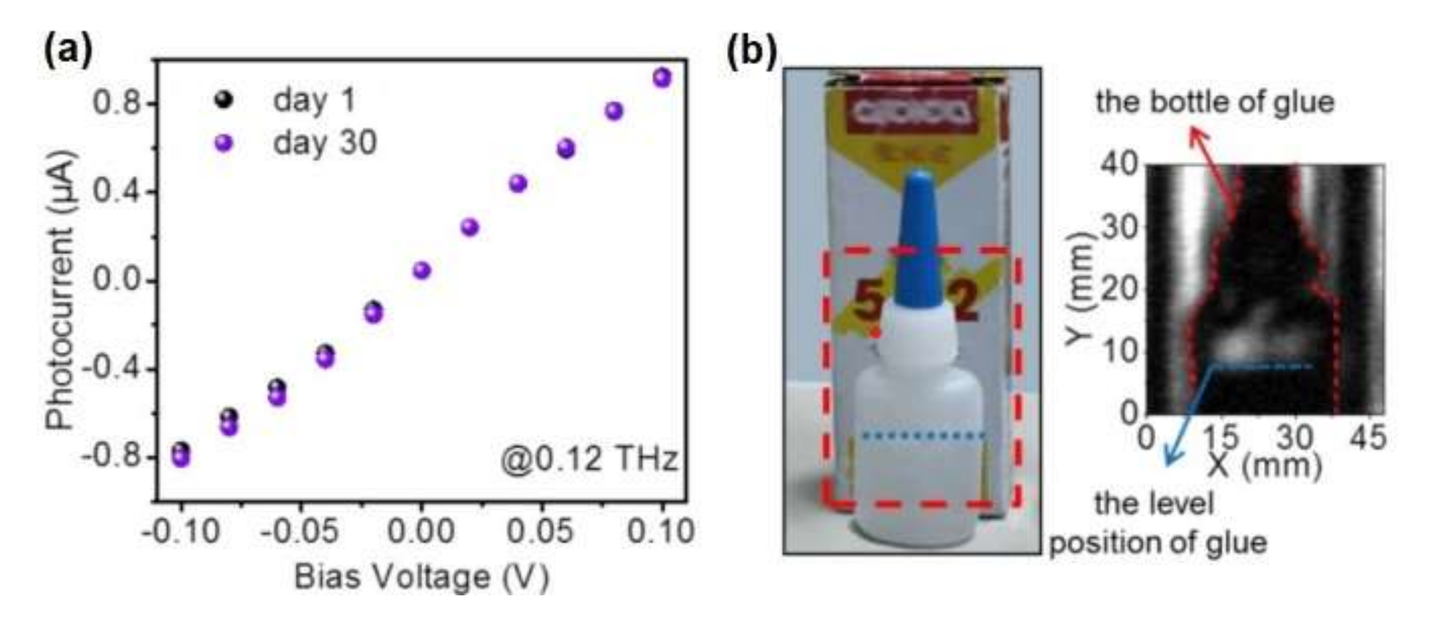
3.4. SnSe2-Based Sensors for Large-Area Imaging with Millimetre Waves

An efficient THz detector at room temperature needs two characteristics: high mobility and a channel with nanometer length in a FET. Alternatively, the electron heat-driven detection mechanism could be used [86], based on the specific geometry of the device and the thermal/electrical properties of the material. In fact, SnSe2 has both a high thermoelectric power and a suitable bandgap [87], which are advantageous characteristics for the production of hot electrons and for photothermal conversion. To improve the THz photodetection performance of the SnSe2-based device, the relationship between channel length and photoresponse should be investigated. In FETs, an important issue concerning THz detection is that the channel length should be less than tens of nanometers at the expense of rectification ratio. As mentioned above, it is possible to exploit hot electrons to overcome this limit, related to the absorption efficiency of photons. Specifically, the performance of SnSe2-based THz detectors with a channel length of 6 µm and 100 nm, along with the simulated electric field intensity, were evaluated (Figure 11a). A short channel SnSe2 device is reported in Figure 11a-i,ii. In Figure 11a-iii, one can notice how the reduction of the antenna gap increases the value of the square of the electric field intensity (E02) in the channel by almost three orders of magnitude. To study the different photoelectric properties of the devices as a function of the channel length, the photocurrent, the response time, and the reactivity were measured simultaneously using two radiations 0.04 and 0.12 THz with a power density of 2.5 and 1 mW cm−2, respectively. The photocurrent increases linearly under electrical bias as VDS from −0.1 to 0.1 (Figure 11b), due to the increased carrier drift-velocity and reduced carrier transit time. Moreover, the short channel devices show a photocurrent greater than three orders of magnitude at 0.04 THz, congruently with the theoretical predictions of Figure 11a-iii. By exploiting the antenna gap in short channel device, it is possible to concentrate the THz radiation in a very small spot, consequently improving the SnSe2 intraband absorption capacity, thus hot carriers can be efficiently produced [88]. In Figure 11c, one can observe a good linearity over a wide range of the photocurrent, of the short channel device, as a function of the incident power. Using the equation Iph ∝ Pβ to fit the experimental data, β is ~0.98 under positive or negative bias, which is an interesting value for high-contrast imaging. Even at the frequency of 0.12 THz, there is the same improvement effect, as evident from Figure 11d, confirming the broadband nature of THz field nano-focusing. Additionally, the response time at 0.12 THz for both short and long channel devices was also studied (Figure 11e). For the short channel device, τrise =2.7µs and τfall = 2.3 µs—i.e., a response time of approximately 16 times faster than in the long channel device (τrise = 45.4 µs, τfall = 46.5 µs). Obviously, the long channel device has a slower response time than the short channel device, making the short channel device advantageous in applications. The increase in VDS rapidly increases the bias voltage response to 0.12 THz (Figure 11f). For short channel devices, the maximum response is 2.5 A W−1, which is approximately five times larger than graphene-based devices (20 V W−1) [89] and 12 times larger than black-phosphorus-based devices (7.8 V W−1) [90]. This indicates that short-channel SnSe2 devices have superior performance respect to graphene- and black phosphorus-based devices.
Exploiting the excellent performance of the SnSe2, a large area imaging device with THz transmission was created for identifying hidden objects. Using a radiation of 0.12 THz, the shape of the glue-jar in the box was clearly visible (see Figure 12b). Furthermore, it was possible to detect not only the shape of the glue-jar but also the position of the amount of the glue inside the jar. Another key feature of the THz detector is its stability. Differently from black phosphorus [92], SnSe2-based devices exhibited better stability, congruently with the ambient stability assessed in Figure 6 by surface-science techniques. The absence of noticeable modifications in the photocurrent at 0.12 THz radiation after a prolonged storage in air (extended up to one month, Figure 12a) corroborates the excellent stability of SnSe2-based optoelectronic devices.

4. Conclusions

Here, we elucidated the main features of chemical reactivity of SnSe2. While the stoichiometric single crystal is chemically inert to ambient gases, the presence of selenium vacancies drastically affects surface chemical reactivity. The SnSe2−x surface is transformed into SnO2-skin-terminated SnSe2, with a thickness of the SnO2 skin estimated to be sub-nanometric.
Interestingly, while the self-assembled SnO2/SnSe2-x heterostructure is an exceptional platform for detecting chemical species, as demonstrated for H2, H2O, NO2, NH3, and HS2, the pristine SnSe2 is unable to detect the same species. Thus, our results highlight the pivotal role of Se vacancies in metal dichalcogenides, which can transform the system from ambient-stable to an ultrasensitive gas sensor by tuning the stoichiometry.
Sensitivities of 0.43, 2.13, 0.11, and 1.06 [ppm]−1 were reported for the detection of H2, H2S, NH3, and NO2, respectively. The corresponding limit of detection is 5 ppm, 10 ppb, 250 ppb, and 400 ppb for H2, H2S, NH3, and NO2, respectively.
Moreover, SnSe2 is particularly suitable for THz photodetection, based on hot electrons. The response speed and the reactivity of the device are significantly improved thanks to the short channel, which exploits the localization of the electrostatic field and the high thermoelectric value of SnSe2. Furthermore, the device has excellent stability, even when the uncapped active channel is exposed to air for long periods, thanks to the exceptional chemical inertness of the single stoichiometric SnSe2 crystals. Accordingly, SnSe2-based photodetectors represent suitable and promising candidates for imaging applications for homeland security and quality controls.

Supplementary Materials

The following supporting information can be downloaded at: https://www.mdpi.com/article/10.3390/ma15031154/s1, File S1: Theoretical Methods; File S2: Fabrication process and measurements of devices.

Author Contributions

Conceptualization, A.P., D.W.B., D.F., and G.D.; Methodology, C.-N.K., L.O., and C.S.L.; Investigation, D.W.B. and D.F.; Resources, D.F. and L.O.; Data curation, G.D. and D.F.; Writing—original draft preparation, G.D.; Writing—review and editing, G.D. and A.P.; Supervision, A.P. All authors have read and agreed to the published version of the manuscript.

Funding

We acknowledge financial support from the Spanish Ministry of Science and Innovation, through project PID2019-109525RB-I00.

Conflicts of Interest

The authors declare no conflict of interest.

References

  1. Novoselov, K. Nobel Lecture: Graphene: Materials in the Flatland. Rev. Mod. Phys. 2011, 83, 837–849. [Google Scholar] [CrossRef]
  2. Geim, A.K. Nobel Lecture: Random walk to graphene. Rev. Mod. Phys. 2011, 83, 851–862. [Google Scholar] [CrossRef] [Green Version]
  3. Tao, Y.; Han, B.H.; Sui, Z.Y.; Tao, Y.; Han, B.H. Advanced porous graphene materials: From in-plane pore generation to energy storage applications. J. Mater. Chem. A 2020, 8, 6125–6143. [Google Scholar] [CrossRef]
  4. Yang, L.; Yi, N.; Zhu, J.; Cheng, Z.; Yin, X.; Zhang, X.; Zhu, H.; Cheng, H. Novel gas sensing platform based on a stretchable laser-induced graphene pattern with self-heating capabilities. J. Mater. Chem. A 2020, 8, 6487–6500. [Google Scholar] [CrossRef]
  5. Ahmadi, M.; Zabihi, O.; Jeon, S.; Yoonessi, M.; Dasari, A.; Ramakrishna, S.; Naebe, M. 2D transition metal dichalcogenide nanomaterials: Advances, opportunities, and challenges in multi-functional polymer nanocomposites. J. Mater. Chem. A 2020, 8, 845–883. [Google Scholar] [CrossRef]
  6. Jalil, A.; Zhuo, Z.; Sun, Z.; Wu, F.; Wang, C.; Wu, X. A phosphorene-like InP3 monolayer: Structure, stability, and catalytic properties toward the hydrogen evolution reaction. J. Mater. Chem. A 2020, 8, 1307–1314. [Google Scholar] [CrossRef]
  7. Wu, J.; Liu, J.; Cui, J.; Yao, S.; Ihsan-Ul-Haq, M.; Mubarak, N.; Quattrocchi, E.; Ciucci, F.; Kim, J.-K. Dual-phase MoS2 as a high-performance sodium-ion battery anode. J. Mater. Chem. A 2020, 8, 2114–2122. [Google Scholar] [CrossRef]
  8. Zeng, L.; Li, X.; Chen, S.; Wen, J.; Huang, W.; Chen, A. Unique hollow Ni-Fe@MoS2 nanocubes with boosted electrocat-alytic activity for N2 reduction to NH3. J. Mater. Chem. A 2020, 8, 7339–7349. [Google Scholar] [CrossRef]
  9. Zu, G.; Guo, G.; Li, H.; Lu, Y.; Wang, R.; Hu, Y.; Wang, L.; Wang, J. Revealing the failure mechanism of transition-metal chalcogenides towards the copper current collector in secondary batteries. J. Mater. Chem. A 2020, 8, 6569–6575. [Google Scholar] [CrossRef]
  10. Hu, G.; Fung, V.; Sang, X.; Unocic, R.R.; Ganesh, P. Superior electrocatalytic hydrogen evolution at engineered non-stoichiometric two-dimensional transition metal dichalcogenide edges. J. Mater. Chem. A 2019, 7, 18357–18364. [Google Scholar] [CrossRef]
  11. Li, J.; Hong, W.; Jian, C.; Cai, Q.; He, X.; Liu, W. High-performance hydrogen evolution at a MoSe2-Mo2C seamless heterojunction enabled by efficient charge transfer. J. Mater. Chem. A 2020, 8, 6692–6698. [Google Scholar] [CrossRef]
  12. Hu, H.; Shi, Z.; Khan, K.; Cao, R.; Liang, W.; Tareen, A.K.; Zhang, Y.; Huang, W.; Guo, Z.; Luo, X.; et al. Recent advances in doping engineering of black phosphorus. J. Mater. Chem. A 2020, 8, 5421–5441. [Google Scholar] [CrossRef]
  13. Ozawa, A.; Yamamoto, M.; Tanabe, T.; Hosokawa, S.; Yoshida, T. Black phosphorus synthesized by solvothermal reaction from red phosphorus and its catalytic activity for water splitting. J. Mater. Chem. A 2020, 8, 7368–7376. [Google Scholar] [CrossRef]
  14. Tian, Y.; Wang, H.; Li, H.; Guo, Z.; Tian, B.; Cui, Y.; Li, Z.; Li, G.; Zhang, H.; Wu, Y. Recent advances in black phosphorus/carbon hybrid composites: From improved stability to applications. J. Mater. Chem. A 2020, 8, 4647–4676. [Google Scholar] [CrossRef]
  15. Ghosh, B.; Kumar, P.; Thakur, A.; Chauhan, Y.S.; Bhowmick, S.; Agarwal, A. Anisotropic plasmons, excitons, and electron energy loss spectroscopy of phosphorene. Phys. Rev. B 2017, 96, 035422. [Google Scholar] [CrossRef] [Green Version]
  16. Sadhukhan, K.; Agarwal, A. Anisotropic plasmons, Friedel oscillations, and screening in 8-Pmmn borophene. Phys. Rev. B 2017, 96, 035410. [Google Scholar] [CrossRef] [Green Version]
  17. Ottaviano, L.; Palleschi, S.; Perrozzi, F.; D’Olimpio, G.; Priante, F.; Donarelli, M.; Benassi, P.; Nardone, M.; Gonchigsuren, M.; Gombosuren, M.; et al. Mechanical exfoliation and layer number identification of MoS2 revisited. 2D Mater. 2017, 4, 045013. [Google Scholar] [CrossRef]
  18. Yi, M.; Shen, Z. A review on mechanical exfoliation for the scalable production of graphene. J. Mater. Chem. A 2015, 3, 11700–11715. [Google Scholar] [CrossRef]
  19. Gibaja, C.; Assebban, M.; Torres, I.; Fickert, M.; Sanchis-Gual, R.; Brotons-Alcázar, I.; Paz, W.; Palacios, J.J.; Michel, E.G.; Abellán, G.; et al. Liquid phase exfoliation of antimonene: Systematic optimization, characterization and electrocatalytic properties. J. Mater. Chem. A 2019, 7, 22475–22486. [Google Scholar] [CrossRef]
  20. Adilbekova, B.; Lin, Y.; Yengel, E.; Faber, H.; Harrison, G.T.; Firdaus, Y.; El Labban, A.; Anjum, D.H.; Tung, V.; Anthopoulos, T.D. Liquid phase exfoliation of MoS2 and WS2 in aqueous ammonia and their application in highly efficient organic solar cells. J. Mater. Chem. C 2020, 8, 5259–5264. [Google Scholar] [CrossRef] [Green Version]
  21. Hernandez, Y.; Nicolosi, V.; Lotya, M.; Blighe, F.M.; Sun, Z.; De, S.; McGovern, I.T.; Holland, B.; Byrne, M.; Gun’Ko, Y.K.; et al. High-yield production of graphene by liquid-phase exfoliation of graphite. Nat. Nanotechnol. 2008, 3, 563–568. [Google Scholar] [CrossRef] [PubMed] [Green Version]
  22. Jin, Z.; Li, X.; Mullen, J.T.; Kim, K.W. Intrinsic transport properties of electrons and holes in monolayer transition-metal dichalcogenides. Phys. Rev. B 2014, 90, 045422. [Google Scholar] [CrossRef] [Green Version]
  23. Edmonds, M.; Tadich, A.; Carvalho, A.; Ziletti, A.; O’Donnell, K.M.; Koenig, S.P.; Coker, D.F.; Özyilmaz, B.; Neto, A.H.C.; Fuhrer, M. Creating a Stable Oxide at the Surface of Black Phosphorus. ACS Appl. Mater. Interfaces 2015, 7, 14557–14562. [Google Scholar] [CrossRef] [PubMed]
  24. Bergeron, A.; Ibrahim, J.; Leonelli, R.; Francoeur, S. Oxidation dynamics of ultrathin GaSe probed through Raman spectroscopy. Appl. Phys. Lett. 2017, 110, 241901. [Google Scholar] [CrossRef]
  25. Shi, L.; Li, Q.; Ouyang, Y.; Wang, J. Effect of illumination and Se vacancies on fast oxidation of ultrathin gallium selenide. Nanoscale 2018, 10, 12180–12186. [Google Scholar] [CrossRef]
  26. Lan, Y.; Chen, X.; Hu, C.; Cheng, Y.; Chen, Q. Penta-PdX2 (X = S, Se, Te) monolayers: Promising anisotropic thermoelectric materials. J. Mater. Chem. A 2019, 7, 11134–11142. [Google Scholar] [CrossRef]
  27. Wu, D.; Jia, C.; Shi, F.; Zeng, L.; Lin, P.; Dong, L.; Shi, Z.; Tian, Y.; Li, X.; Jie, J. Mixed-dimensional PdSe2/SiNWA hetero-structure based photovoltaic detectors for self-driven, broadband photodetection, infrared imaging and humidity sensing. J. Mater. Chem. A 2020, 8, 3632–3642. [Google Scholar] [CrossRef]
  28. Yu, B.; Qi, F.; Zheng, B.; Hou, W.; Zhang, W.; Li, Y.; Chen, Y. Self-assembled pearl-bracelet-like CoSe2-SnSe2/CNT hollow architecture as highly efficient electrocatalysts for hydrogen evolution reaction. J. Mater. Chem. A 2018, 6, 1655–1662. [Google Scholar] [CrossRef]
  29. Wei, Z.; Wang, L.; Zhuo, M.; Ni, W.; Wang, H.; Ma, J. Layered tin sulfide and selenide anode materials for Li- and Na-ion batteries. J. Mater. Chem. A 2018, 6, 12185–12214. [Google Scholar] [CrossRef]
  30. Huang, Y.; Ling, C.; Liu, H.; Wang, S. Tuning electronic and magnetic properties of SnSe2 armchair nanoribbons via edge hydrogenation. J. Mater. Chem. C 2014, 2, 10175–10183. [Google Scholar] [CrossRef]
  31. Li, W.; Xiong, L.; Li, N.; Pang, S.; Xu, G.; Yi, C.; Wang, Z.; Gu, G.; Li, K.; Li, W.; et al. Tunable 3D light trapping architectures based on self-assembled SnSe2 nanoplate arrays for ultrasensitive SERS detection. J. Mater. Chem. C 2019, 7, 10179–10186. [Google Scholar] [CrossRef]
  32. Shafique, A.; Samad, A.; Shin, Y.-H. Ultra low lattice thermal conductivity and high carrier mobility of monolayer SnS2and SnSe2: A first principles study. Phys. Chem. Chem. Phys. 2017, 19, 20677–20683. [Google Scholar] [CrossRef] [PubMed]
  33. Shao, Z.; Fu, Z.-G.; Li, S.; Cao, Y.; Bian, Q.; Sun, H.; Zhang, Z.; Gedeon, H.; Zhang, X.; Liu, L.; et al. Strongly Compressed Few-Layered SnSe2 Films Grown on a SrTiO3 Substrate: The Coexistence of Charge Ordering and Enhanced Interfacial Superconductivity. Nano Lett. 2019, 19, 5304–5312. [Google Scholar] [CrossRef] [PubMed]
  34. Zeng, J.; Liu, E.; Fu, Y.; Chen, Z.; Pan, C.; Wang, C.; Wang, M.; Wang, Y.; Xu, K.; Cai, S.; et al. Gate-Induced Interfacial Superconductivity in 1T-SnSe2. Nano Lett. 2018, 18, 1410–1415. [Google Scholar] [CrossRef] [PubMed] [Green Version]
  35. Kim, S.; Yao, Z.; Lim, J.-M.; Hersam, M.C.; Wolverton, C.; Dravid, V.P.; He, K. Lithium-Ion Batteries: Atomic-Scale Observation of Electrochemically Reversible Phase Transformations in SnSe2 Single Crystals. Adv. Mater. 2018, 30, 1870393. [Google Scholar] [CrossRef] [Green Version]
  36. Zhang, F.; Xia, C.; Zhu, J.; Ahmed, B.; Liang, H.; Velusamy, D.B.; Schwingenschlögl, U.; Alshareef, H.N. SnSe22D Anodes for Advanced Sodium Ion Batteries. Adv. Energy Mater. 2016, 6, 1601188. [Google Scholar] [CrossRef]
  37. Zhou, X.; Zhou, N.; Li, C.; Song, H.; Zhang, Q.; Hu, X.; Gan, L.; Li, H.; Lü, J.; Luo, J.; et al. Vertical heterostructures based on SnSe2/MoS2 for high performance photodetectors. 2D Mater. 2017, 4, 025048. [Google Scholar] [CrossRef]
  38. Fan, Y.; Wang, J.; Zhao, M. Spontaneous full photocatalytic water splitting on 2D MoSe2/SnSe2 and WSe2/SnSe2 vdW heterostructures. Nanoscale 2019, 11, 14836–14843. [Google Scholar] [CrossRef]
  39. Tan, P.; Chen, X.; Wu, L.; Shang, Y.Y.; Liu, W.; Pan, J.; Xiong, X. Hierarchical flower-like SnSe2 supported Ag3PO4 nanoparticles: Towards visible light driven photocatalyst with enhanced performance. Appl. Catal. B: Environ. 2017, 202, 326–334. [Google Scholar] [CrossRef] [Green Version]
  40. Wang, M.; Wang, Z.; Xu, X.; Duan, S.; Du, C. Tin diselenide-based saturable absorbers for eye-safe pulse lasers. Nanotechnology 2019, 30, 265703. [Google Scholar] [CrossRef]
  41. Zhang, Y.; Liu, Y.; Lim, K.H.; Xing, C.; Li, M.; Zhang, T.; Tang, P.; Arbiol, J.; Llorca, J.; Ng, K.M.; et al. Tin Diselenide Molecular Precursor for Solution-Processable Thermoelectric Materials. Angew. Chem. Int. Ed. 2018, 57, 17063–17068. [Google Scholar] [CrossRef] [PubMed]
  42. Luo, Y.; Zheng, Y.; Luo, Z.; Hao, S.; Du, C.; Liang, Q.; Li, Z.; Khor, K.A.; Hippalgaonkar, K.; Xu, J.; et al. n-Type SnSe2 Oriented-Nanoplate-Based Pellets for High Thermoelectric Performance. Adv. Energy Mater. 2018, 8, 1702167. [Google Scholar] [CrossRef]
  43. Lee, Y.K.; Luo, Z.-Z.; Cho, S.P.; Kanatzidis, M.G.; Chung, I. Surface Oxide Removal for Polycrystalline SnSe Reveals Near-Single-Crystal Thermoelectric Performance. Joule 2019, 3, 719–731. [Google Scholar] [CrossRef] [Green Version]
  44. Lamuta, C.; Campi, D.; Pagnotta, L.; Dasadia, A.; Cupolillo, A.; Politano, A. Determination of the mechanical properties of SnSe, a novel layered semiconductor. J. Phys. Chem. Solids 2018, 116, 306–312. [Google Scholar] [CrossRef]
  45. Yamashita, A.; Ogiso, O.; Matsumoto, R.; Tanaka, M.; Hara, H.; Tanaka, H.; Takeya, H.; Lee, C.-H.; Takano, Y. Influence of Oxidation in Starting Material Sn on Electric Transport Properties of SnSe Single Crystals. J. Phys. Soc. Jpn. 2018, 87, 065001. [Google Scholar] [CrossRef]
  46. Chung, K.-M.; Wamwangi, D.M.; Woda, M.; Wuttig, M.; Bensch, W. Investigation of SnSe, SnSe2, and Sn2Se3 alloys for phase change memory applications. J. Appl. Phys. 2008, 103, 083523. [Google Scholar] [CrossRef]
  47. Guo, C.; Tian, Z.; Xiao, Y.; Mi, Q.; Xue, J. Field-effect transistors of high-mobility few-layer SnSe2. Appl. Phys. Lett. 2016, 109, 203104. [Google Scholar] [CrossRef] [Green Version]
  48. Palosz, B.; Salje, E. Lattice parameters and spontaneous strain in AX2 polytypes: CdI2, PbI2 SnS2 and SnSe2. J. Appl. Crystallogr. 1989, 22, 622–623. [Google Scholar] [CrossRef]
  49. Evans, B.L.; Hazelwood, R.A. Optical and electrical properties of SnSe2. J. Phys. D: Appl. Phys. 1969, 2, 1507–1516. [Google Scholar] [CrossRef]
  50. Mead, D.G.; Irwin, J.C. Raman spectra of SnS2 and SnSe2. Solid State Commun. 1976, 20, 885–887. [Google Scholar] [CrossRef]
  51. Smith, A.J.; Meek, P.E.; Liang, W.Y. Raman scattering studies of SnS2 and SnSe2. J. Phys. C Solid State Phys. 1977, 10, 1321–1323. [Google Scholar] [CrossRef]
  52. Taube, A.; Łapińska, A.; Judek, J.; Zdrojek, M. Temperature dependence of Raman shifts in layered ReSe2 and SnSe2 semiconductor nanosheets. Appl. Phys. Lett. 2015, 107, 013105. [Google Scholar] [CrossRef]
  53. Henderson, M. The interaction of water with solid surfaces: Fundamental aspects revisited. Surf. Sci. Rep. 2002, 46, 1–308. [Google Scholar] [CrossRef]
  54. Inamdar, A.N.; Som, N.N.; Pratap, A.; Jha, P.K. Hydrogen evolution and oxygen evolution reactions of pristine and alkali metal doped SnSe2 monolayer. Int. J. Hydrogen Energy 2020, 45, 18657–18665. [Google Scholar] [CrossRef]
  55. Deng, J.; Mo, Y.; Liu, J.; Guo, R.; Zhang, Y.; Xue, W.; Zhang, Y. In Vitro Study of SnS2, BiOCl and SnS2-Incorporated BiOCl Inorganic Nanoparticles Used as Doxorubicin Carrier. J. Nanosci. Nanotechnol. 2016, 16, 5740–5745. [Google Scholar] [CrossRef] [PubMed]
  56. Cox, P.; Egdell, R.; Flavell, W.; Helbig, R. Observation of surface optical phonons on SnO2 (110). Vacuum 1983, 33, 835–838. [Google Scholar] [CrossRef]
  57. Nehasil, V.; Janeček, P.; Korotchenkov, G.; Matolin, V. Investigation of behaviour of Rh deposited onto polycrystalline SnO2 by means of TPD, AES and EELS. Surf. Sci. 2003, 532–535, 415–419. [Google Scholar] [CrossRef]
  58. Tanuma, S.; Powell, C.J.; Penn, D.R. Calculations of electron inelastic mean free paths (IMFPS). IV. Evaluation of calculated IMFPs and of the predictive IMFP formula TPP-2 for electron energies between 50 and 2000 eV. Surf. Interface Anal. 1993, 20, 77–89. [Google Scholar] [CrossRef]
  59. Cox, D.F.; Hoflund, G.B. An electronic and structural interpretation of tin oxide ELS spectra. Surf. Sci. 1985, 151, 202–220. [Google Scholar] [CrossRef]
  60. Wu, S.; Liu, C.; Wu, Z.; Miao, L.; Gao, J.; Hu, X.; Chen, J.; Zheng, Y.; Wang, X.; Shen, C.; et al. Realizing tremendous electrical transport properties of polycrystalline SnSe2 by Cl-doped and anisotropy. Ceram. Int. 2019, 45, 82–89. [Google Scholar] [CrossRef]
  61. Nagaraju, G.; Cha, S.M.; Sekhar, S.C.; Yu, J.S. Metallic Layered Polyester Fabric Enabled Nickel Selenide Nanostructures as Highly Conductive and Binderless Electrode with Superior Energy Storage Performance. Adv. Energy Mater. 2017, 7. [Google Scholar] [CrossRef]
  62. Al-Hada, N.M.; Kamari, H.M.; Baqer, A.A.; Shaari, A.H.; Saion, E. Thermal Calcination-Based Production of SnO2 Nanopowder: An Analysis of SnO2 Nanoparticle Characteristics and Antibacterial Activities. Nanomaterials 2018, 8, 250. [Google Scholar] [CrossRef] [Green Version]
  63. Zhang, W.; Li, M.; Xiao, X.; Huang, X.; Jiang, Y.; Fan, X.; Chen, L. In situ synthesis of ultrasmall SnO2 quantum dots on nitrogen-doped reduced graphene oxide composite as high performance anode material for lithium-ion batteries. J. Alloys Compd. 2017, 727, 1–7. [Google Scholar] [CrossRef]
  64. Bachvarova-Nedelcheva, A.; Iordanova, R.; Kostov, K.; Yordanov, S.; Ganev, V. Structure and properties of a non-traditional glass containing TeO2, SeO2 and MoO3. Opt. Mater. 2012, 34, 1781–1787. [Google Scholar] [CrossRef]
  65. Wakita, T.; Paris, E.; Kobayashi, K.; Terashima, K.; Hacisalihoǧlu, M.Y.; Ueno, T.; Bondino, F.; Magnano, E.; Píš, I.; Olivi, L.; et al. The electronic structure of Ag1−xSn1 + xSe2 (x = 0.0, 0.1, 0.2, 0.25 and 1.0). Phys. Chem. Chem. Phys. 2017, 19, 26672–26678. [Google Scholar] [CrossRef] [PubMed]
  66. Cimino, A.; Gazzoli, D.; Valigi, M. XPS quantitative analysis and models of supported oxide catalysts. J. Electron Spectrosc. Relat. Phenom. 1999, 104, 1–29. [Google Scholar] [CrossRef]
  67. Park, J.H.; Vishwanath, S.; Wolf, S.; Zhang, K.; Kwak, I.; Edmonds, M.; Breeden, M.; Liu, X.; Dobrowolska, M.; Furdyna, J.; et al. Selective Chemical Response of Transition Metal Dichalcogenides and Metal Dichalcogenides in Ambient Conditions. ACS Appl. Mater. Interfaces 2017, 9, 29255–29264. [Google Scholar] [CrossRef] [PubMed]
  68. Paolucci, V.; D’Olimpio, G.; Kuo, C.-N.; Lue, C.S.; Boukhvalov, D.W.; Cantalini, C.; Politano, A. Self-Assembled SnO2/SnSe2 Heterostructures: A Suitable Platform for Ultrasensitive NO2 and H2 Sensing. ACS Appl. Mater. Interfaces 2020, 12, 34362–34369. [Google Scholar] [CrossRef]
  69. Tian, K.; Wang, X.-X.; Yu, Z.-Y.; Li, H.-Y.; Guo, X. Hierarchical and Hollow Fe2O3 Nanoboxes Derived from Metal–Organic Frameworks with Excellent Sensitivity to H2S. ACS Appl. Mater. Interfaces 2017, 9, 29669–29676. [Google Scholar] [CrossRef]
  70. Wang, T.; Wang, Y.; Sun, Q.; Zheng, S.; Liu, L.; Li, J.; Hao, J. Boosted interfacial charge transfer in SnO2/SnSe2 hetero-structures: Toward ultrasensitive room-temperature H2S detection. Inorg. Chem. Front. 2021, 8, 2068–2077. [Google Scholar] [CrossRef]
  71. Zhang, D.; Wu, Z.; Zong, X. Flexible and highly sensitive H2S gas sensor based on in-situ polymerized SnO2/rGO/PANI ternary nanocomposite with application in halitosis diagnosis. Sens. Actuators B Chem. 2019, 289, 32–41. [Google Scholar] [CrossRef]
  72. Liu, L.; Wang, Y.; Dai, Y.; Li, G.; Wang, S.; Li, T.; Zhang, T.; Qin, S. In situ growth of NiO@SnO2 hierarchical nanostructures for high performance H2S sensing. ACS Appl. Mater. Interfaces 2019, 11, 44829–44836. [Google Scholar] [CrossRef] [PubMed]
  73. Gao, X.; Ouyang, Q.; Zhu, C.; Zhang, X.; Chen, Y. Porous MoO3/SnO2 Nanoflakes with n–n Junctions for Sensing H2S. ACS Appl. Nano Mater. 2019, 2, 2418–2425. [Google Scholar] [CrossRef]
  74. Eom, N.S.A.; Cho, H.-B.; Song, Y.; Go, G.M.; Lee, J.; Choa, Y.-H. Room-temperature H2S gas sensing by selectively synthesized Cux(x=1, 2)O: SnO2 thin film nanocomposites with oblique & vertically assembled SnO2 ceramic nanorods. Sens. Actuators B Chem. 2018, 273, 1054–1061. [Google Scholar]
  75. Shen, Y.; Yamazaki, T.; Liu, Z.; Meng, D.; Kikuta, T.; Nakatani, N.; Saito, M.; Mori, M. Microstructure and H2 gas sensing properties of undoped and Pd-doped SnO2 nanowires. Sens. Actuators B Chem. 2009, 135, 524–529. [Google Scholar] [CrossRef]
  76. Ghimbeu, C.M.; Lumbreras, M.; Siadat, M.; van Landschoot, R.C.; Schoonman, J. Electrostatic sprayed SnO2 and Cu-doped SnO2 films for H2S detection. Sens. Actuators B Chem. 2008, 133, 694–698. [Google Scholar] [CrossRef]
  77. Guo, X.; Ding, Y.; Liang, C.; Du, B.; Zhao, C.; Tan, Y.; Shi, Y.; Zhang, P.; Yang, X.; He, Y. Humidity-activated H2S sensor based on SnSe2/WO3 composite for evaluating the spoilage of eggs at room temperature. Sens. Actuators B Chem. 2022, 357, 131424. [Google Scholar] [CrossRef]
  78. Song, Z.; Wei, Z.; Wang, B.; Luo, Z.; Xu, S.; Zhang, W.; Yu, H.; Li, M.; Huang, Z.; Zang, J.; et al. Sensitive Room-Temperature H2S Gas Sensors Employing SnO2 Quantum Wire/Reduced Graphene Oxide Nanocomposites. Chem. Mater. 2016, 28, 1205–1212. [Google Scholar] [CrossRef]
  79. Moreira, L.C.; Cheng, W.-Y.; Fuh, H.-R.; Chien, W.-C.; Yan, W.; Fei, H.; Xu, H.; Zhang, D.; Chen, Y.; Zhao, Y.; et al. High Selectivity Gas Sensing and Charge Transfer of SnSe2. ACS Sens. 2019, 4, 2546–2552. [Google Scholar] [CrossRef]
  80. Pan, Q.; Li, T.; Zhang, D. Ammonia gas sensing properties and density functional theory investigation of coral-like Au-SnSe2 Schottky junction. Sens. Actuators B Chem. 2021, 332, 129440. [Google Scholar] [CrossRef]
  81. Rani, S.; Kumar, M.; Singh, Y.; Tomar, M.; Sharma, A.; Gupta, V.; Singh, V.N. NO2 Gas Sensor Based on SnSe/SnSe2p-n Hetrojunction. J. Nanosci. Nanotechnol. 2021, 21, 4779–4785. [Google Scholar] [CrossRef] [PubMed]
  82. Lee, L.; Chen, C.-W.; Manikandan, A.; Lee, S.-H.; Wang, Z.M.; Chueh, Y.-L. Phase-engineered SnSex toward SnSe2/SnSe heterostructure with improved thermal conductance by a low-temperature plasma-assisted chemical vapor reaction. Nano Energy 2018, 44, 419–429. [Google Scholar] [CrossRef]
  83. Liu, W.; Gu, D.; Li, X. AuPt Bimetal-Functionalized SnSe2 Microflower-Based Sensors for Detecting Sub-ppm NO2 at Low Temperatures. ACS Appl. Mater. Interfaces 2021, 13, 20336–20348. [Google Scholar] [CrossRef]
  84. Wang, X.; Liu, Y.; Dai, J.; Chen, Q.; Huang, X.; Huang, W. Solution-Processed p-SnSe/n-SnSe2 Hetero-Structure Layers for Ultrasensitive NO2 Detection. Chem. Eur. J. 2020, 26, 3870–3876. [Google Scholar] [CrossRef]
  85. Li, X.; Liu, W.; Huang, B.; Liu, H.; Li, X. Layered SnSe2 microflakes and SnSe2/SnO2 heterojunctions for low-temperature chemiresistive-type gas sensing. J. Mat. Chem. C 2020, 8, 15804–15815. [Google Scholar] [CrossRef]
  86. Song, J.C.W.; Rudner, M.S.; Marcus, C.M.; Levitov, L.S. Hot Carrier Transport and Photocurrent Response in Graphene. Nano Lett. 2011, 11, 4688–4692. [Google Scholar] [CrossRef] [Green Version]
  87. Su, Y.; Ebrish, M.A.; Olson, E.J.; Koester, S.J. SnSe2 field-effect transistors with high drive current. Appl. Phys. Lett. 2013, 103, 263104. [Google Scholar] [CrossRef]
  88. Mics, Z.; Tielrooij, K.-J.; Parvez, K.; Jensen, S.A.; Ivanov, I.; Feng, X.; Müllen, K.; Bonn, M.; Turchinovich, D. Thermodynamic picture of ultrafast charge transport in graphene. Nat. Commun. 2015, 6, 7655. [Google Scholar] [CrossRef] [Green Version]
  89. Bandurin, D.A.; Gayduchenko, I.; Cao, Y.; Moskotin, M.; Principi, A.; Grigorieva, I.V.; Goltsman, G.; Fedorov, G.; Svintsov, D. Dual origin of room temperature sub-terahertz photoresponse in graphene field effect transistors. Appl. Phys. Lett. 2018, 112, 141101. [Google Scholar] [CrossRef] [Green Version]
  90. Viti, L.; Hu, J.; Coquillat, D.; Politano, A.; Knap, W.; Vitiello, M.S. Efficient Terahertz detection in black-phosphorus nano-transistors with selective and controllable plasma-wave, bolometric and thermoelectric response. Sci. Rep. 2016, 6, 20474. [Google Scholar] [CrossRef] [Green Version]
  91. Guo, C.; Guo, W.; Xu, H.; Zhang, L.; Chen, G.; D’Olimpio, G.; Kuo, C.-N.; Lue, C.S.; Wang, L.; Politano, A.; et al. Ultra-sensitive Ambient-Stable SnSe2-based Broadband Photodetectors for Room-Temperature IR/THz Energy conversion and Imaging. 2D Mater. 2020, 7, 035026. [Google Scholar] [CrossRef]
  92. Island, J.O.; Steele, G.A.; Van Der Zant, H.S.J.; Castellanos-Gomez, A. Environmental instability of few-layer black phosphorus. 2D Mater. 2015, 2, 011002. [Google Scholar] [CrossRef] [Green Version]
Figure 1. (a) Side and (b) top views of the atomic structure of SnSe2. Green and blue balls denote Se and Sn atoms, respectively. Panel (c) reports the single-crystal XRD pattern from the (001) plane of SnSe2. The inset shows a photograph of an as-grown SnSe2 single crystal. Panel (d) reports the Raman spectrum of SnSe2 single crystal acquired at room temperature with a laser with wavelength λ = 632.8 nm.
Materials 15 01154 g001
Figure 2. Optimized atomic structure of (a) water molecules physisorbed at one Se-vacancy site; (b) decomposed oxygen molecule on SnSe surface layer; (c) metastable SnSe2O2 surface layer; and (d) SnO2-skin-terminated SnSe2.
Materials 15 01154 g002
Figure 3. Vibrational spectra around the energy of O-H intramolecular stretching, recorded upon dosing to 105 L of H2O at T = 300 K the surfaces of various tin-based selenides: SnSe2 (orange), SnSe1.7 (black), SnSe1.4 (green), and SnSe (blue). We also report vibrational acquired in the same conditions for water-dosed InSe (red) and PtTe1.6 (brown). The energy of the primary electron beam is 4 eV.
Materials 15 01154 g003
Figure 4. (a) Vibrational data for oxidized SnSe2(001) (recorded by HREELS with impinging energy of 4 eV) and bulk SnO2(110) (data taken from [56]). (b) Excitation spectrum for pristine and air-modified SnSe2 (recorded by EELS with impinging energy of 300 eV) and bulk SnO2 (data taken from [57]).
Materials 15 01154 g004
Figure 5. Partial densities of states for SnSe2 slab with SnO2-skin (see Figure 2d). Fermi energy is set as zero.
Materials 15 01154 g005
Figure 6. Panels (a) and (b) show Sn-3d and Se-3d core levels for as-cleaved surface of SnSe2 and its modification upon O2 (105 L) dosage and air exposure. The photon energy is 800 eV.
Materials 15 01154 g006
Figure 7. (a) Sn-3d and (b) Se-3d core levels of powderized SnSe2 single crystal. Note that grinding of SnSe2 bulk crystals was carried out in ambient atmosphere. The photon energy is 1486.6 eV (Al Kα).
Materials 15 01154 g007
Figure 8. Panels (a-c) report the change of the charge density after adsorption of one water molecule on SnSe2, one water molecule on SnO2-skin-terminated SnSe2, and two water molecules on SnO2-skin-terminated SnSe2, respectively. Panel (d) represents the DOS of SnO2-skin-terminated SnSe2 (black curve) and of the same system modified by the adsorption of one (red curve) and two (blue curve) water molecules. Fermi level is set at 0.
Materials 15 01154 g008
Figure 9. Change of charge densities after adsorption of (a,c,e) NH3 and (b,d,f) H2S on (a,b) bulk and (c,d) monolayer of SnSe2 and, moreover, (e,f) the SnO2 skin on an underlying SnSe2 substrate.
Materials 15 01154 g009
Figure 10. Dynamic response-recovery curve for NO2 (1 ppm) and NH3 (40 ppm). The inset depicts that electronic charge transfer occurs from SnSe2 to NO2, while the opposite charge transfer exists in the case of NH3, congruently with experimental findings on electrical tests. Reproduced with permission from [79].
Materials 15 01154 g010
Figure 11. (ai) Schematization of the realization of the short-channel device. (aii) Image of a short channel SnSe2-based photodetector acquired with the SEM. (aiii) The electric field distribution of the SnSe2-based long channel (left panel) and short channel (right panel) photodetector. (b) and (c) Photocurrent as a function of the bias voltage and incident power at 0.04 THz, respectively. (d) Photocurrent as a function of bias voltage at 0.12 THz. (e) (top panel) Long channel and (bottom panel) short channel time-resolved photocurrent devices at 0.12 THz with 1 mW cm−2 power. (f) Photoresponsivity vs. bias voltage at 0.12 THz with 1 mW cm−2 power. Reproduced with permission from [91].
Materials 15 01154 g011
Figure 12. (a) Aging in air of SnSe2-based short channel photodetector, black and purple spot represent the photocurrent of as-prepared device and after 30 days in air, respectively. (b) The THz imaging of a glue-jar in the box at 0.12 THz. Reproduced with permission from [91].
Materials 15 01154 g012
Table 1. Differential enthalpy ΔHads and differential Gibbs free energy ΔG for physisorption at room temperature and differential enthalpy of decomposition ΔHdec for molecular oxygen and water on the surface of bulk samples of SnSe2, SnSe1.88, and SnSe. For the decomposition of oxygen, we also report, in parenthesis, the differential enthalpy for the formation of an oxygenated surface and a SnO2-like layer.
SurfaceAdsorbantPhysisorptionDecomposition
ΔHads (kJ/mol)ΔG (kJ/mol)ΔHdec (kJ/mol)
SnSe2O2−17.5−3.2−42.3 (−161.6/~ −40.2)
H2O−13.3+18.0+220.9
SnSe1.88O2−37.6−26.3−135.7 (−99.1/−406.7)
H2O−27.9+3.4+175.6
SnSeO2−11.6−0.2−236.1 (−323.1/+95.4)
H2O−8.1+23.2+82.2
SnO2 skinH2O−119.7−106.7−121.3
Table 2. Differential enthalpy (ΔHphys) and Gibbs free energy (ΔG) at an operational temperature of 200 °C for the physisorption of molecular oxygen at the surface of bulk, bilayer, and monolayer SnSe2 and SnSe1.88. The differential enthalphy for oxygen decomposition (ΔHdec) is also reported. All energies are expressed in kJ/mol.
SystemSurfaceΔHphys
(kJ/mol)
ΔGphys
(kJ/mol)
ΔHdec
(kJ/mol)
BulkSnSe2
SnSe1.88
−17.5
−37.6
+5.24
−14.88
−42.3
−135.7
BilayerSnSe2
SnSe1.88
+38.9
−47.6
+61.6
−24.9
−76.3
−115.5
MonolayerSnSe2
SnSe1.88
+53.1
−59.3
+75.8
−36.6
−56.3
+183.5
Table 3. Differential Gibbs free energies ΔG of physisorption at 200 °C and corresponding values of transferred charge for various combination of considered substrates and analytes
SubstrateAnalyteΔG (kJ/mol)Δe
Bulk SnSe2 (SnSe1.88)H2
H2O
H2S
NH3
NO2
+6.79 (−0.11)
+45.63 (−30.97)
+38.70 (−21.32)
+24.50 (−12.10)
+58.87 (−36.75)
+0.09 (+0.10)
−0.17 (−0.20)
−0.12 (−0.14)
+0.06 (+0.12)
−0.07 (−0.10)
Bilayer SnSe2 (SnSe1.88)H2
H2O
H2S
NH3
NO2
+8.91 (−0.10)
+41.23 (−26.8)
+36.14 (−29.65)
+18.91 (−10.01)
+46.75 (−25.44)
+0.08 (+0.10)
−0.15 (−0.18)
−0.10 (−0.13)
+0.10 (+0.15)
−0.10 (−0.11)
Monolayer SnSe2 (SnSe1.88)H2
H2O
H2S
NH3
NO2
+2.89 (−4.63)
+28.97 (−7.11)
+18.35 (−0.12)
−4.91 (−12.10)
+0.12 (−3.45)
+0.10 (+0.09)
−0.15 (−0.20)
−0.12 (−0.09)
+0.16 (+0.15)
−0.09 (−0.10)
SnO2/SnSe2H2
H2O
H2S
NH3
NO2
−135.61
−60.80
−71.28
−96.20
−127.35
+0.15
−0.43
−0.36
+0.44
−0.25
Table 4. Sensing of H2, H2S, NH3, and NO2 for SnSe2- and SnO2-based systems. The response obtained at the respective operational temperature and gas concentration is reported. RT means room temperature.
GasSensing MaterialsOperationalTemperature (°C)Concentration (ppm)ResponseReference
H2SnO2/SnSe2-x1501003[68]
H2SnO215010005.5[75]
H2SSnO2100101–6[76]
H2SSnSe2RT1010–15[77]
H2SSnO2/SnSe2RT1032[70]
H2SSnO2RT5033[78]
NH3SnO2/SnSe2RT1002[70]
NH3SnSe2 RT402.7[79]
NH3Au-SnSe2RT55.3[80]
NO2SnO2/SnSe2RT103.5[70]
NO2SnO2/SnSe2-x15013.2[68]
NO2SnSe2 RT16[79]
NO2SnSe2 RT5112[81]
NO2SnSe2/SnSeRT175[82]
NO2Au/SnSe213083[83]
NO2Pt-SnSe213083.9[83]
NO2SnSe/SnSe2RT512[84]
NO2SnSe2RT81.4[85]
NO2SnO2100101[76]
Table 5. Sensitivity to H2, H2S, NH3, and NO2 for SnSe2-based sensors, as well as their limit of detection.
GasSensitivity [ppm]−1Limit of Detection
H20.43 ± 0.02 [68]5 ppm at 150 °C [68]
H2S2.13 ± 0.01 [77]10 ppb at RT [70]
NH30.11 ± 0.01 [80]250 ppb at RT [80]
NO21.06 ± 0.03 [68]400 ppb at 150 °C [68]
Publisher’s Note: MDPI stays neutral with regard to jurisdictional claims in published maps and institutional affiliations.

