
Enhanced Surface Plasmon by Clusters in TiO2-Ag Composite
Abstract
:1. Instruction
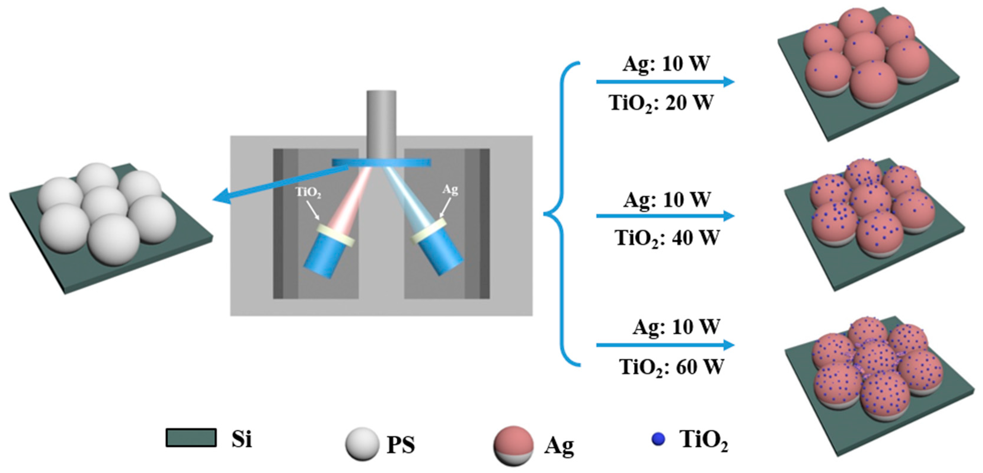
2. Experiment
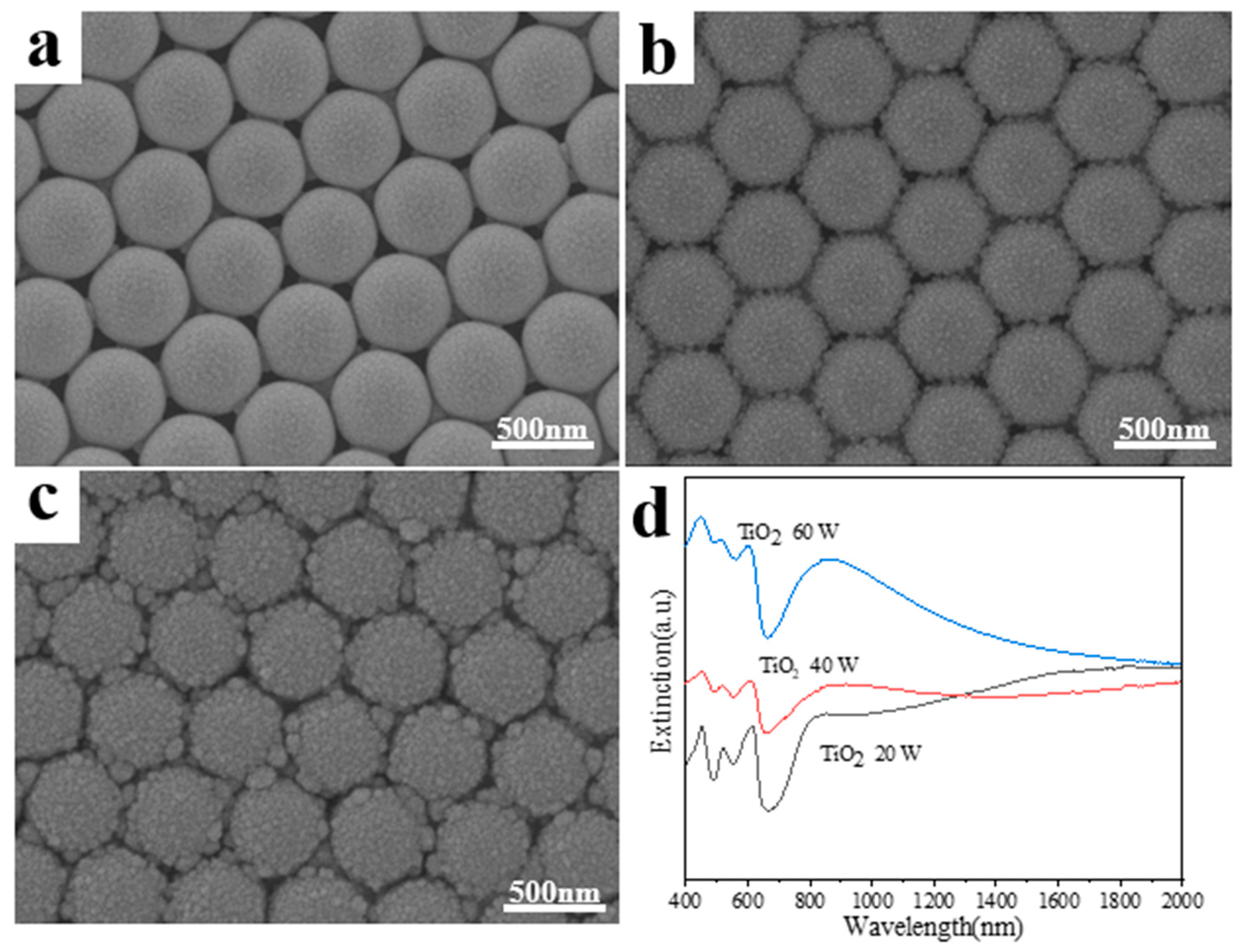
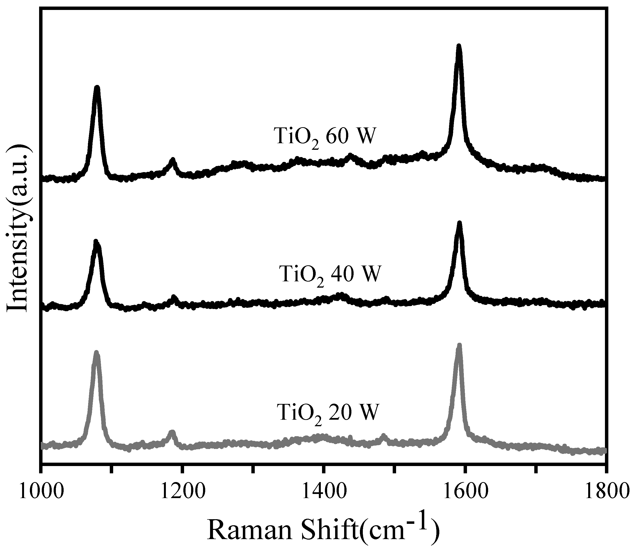
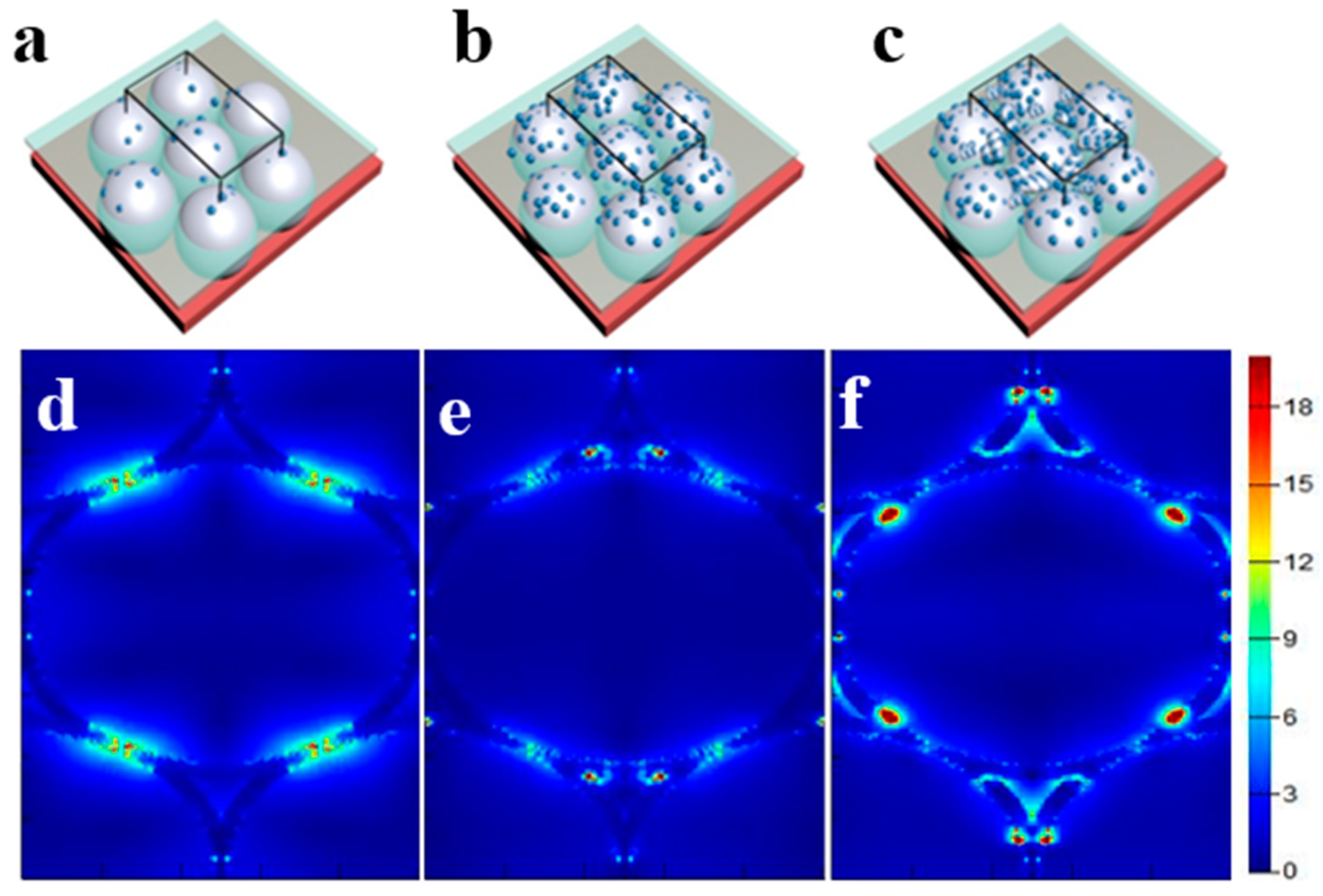
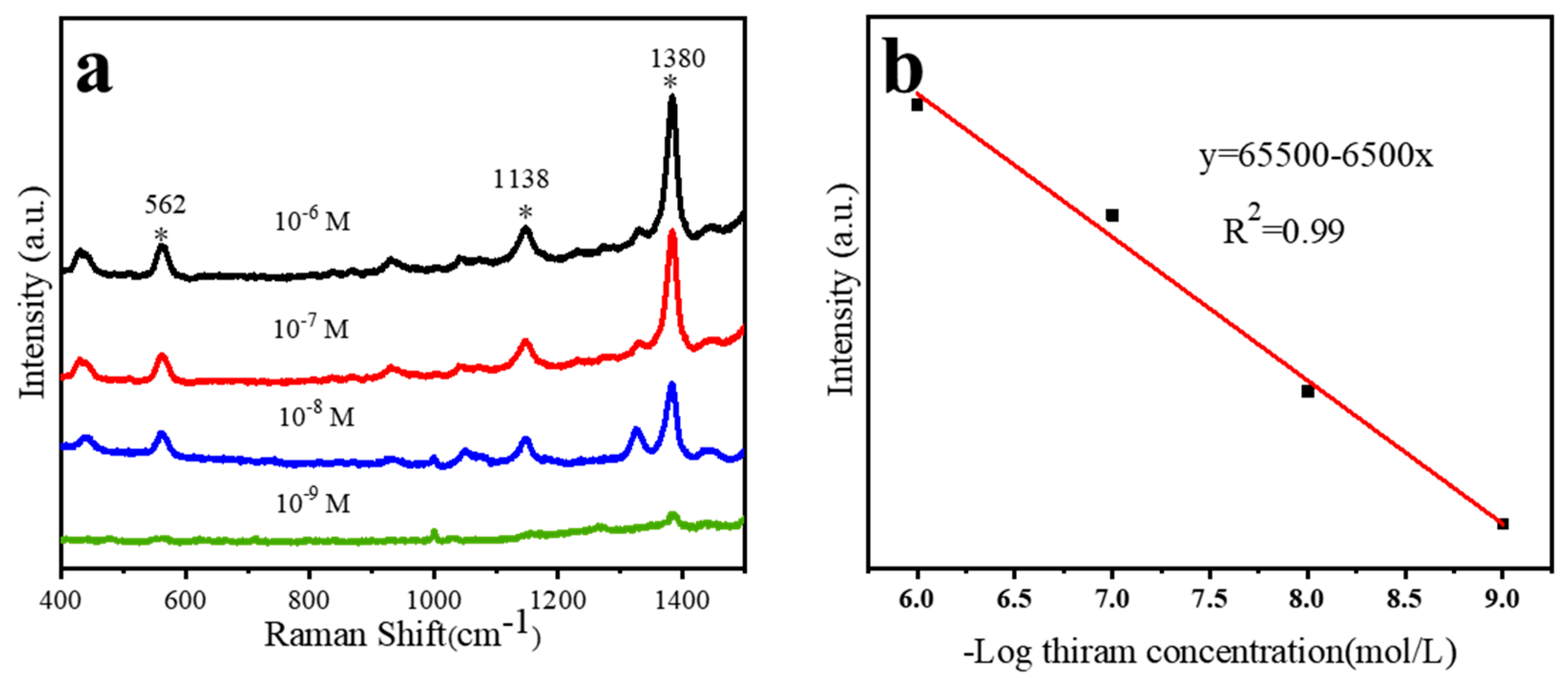
3. Results and Discussion
4. Conclusions
Supplementary Materials
Author Contributions
Funding
Institutional Review Board Statement
Informed Consent Statement
Data Availability Statement
Conflicts of Interest
References
- Yang, Y.; Creedon, N.; O’Riordan, A.; Lovera, P. Surface Enhanced Raman Spectroscopy: Applications in Agriculture and Food Safety. Photonics 2021, 8, 568. [Google Scholar] [CrossRef]
- Balbinot, S.; Srivastav, A.M.; Vidic, J.; Abdulhalim, I.; Manzano, M. Plasmonic biosensors for food control. Trends Food Sci. Technol. 2021, 111, 128–140. [Google Scholar] [CrossRef]
- Baruch Leshem, A.; Isaacs, S.; Srivastava, S.K.; Abdulhalim, I.; Kushmaro, A.; Rapaport, H. Quantitative assessment of paraoxon adsorption to amphiphilic β-sheet peptides presenting the catalytic triad of esterases. J. Colloid Interface Sci. 2018, 530, 328–337. [Google Scholar] [CrossRef]
- Han, H.J.; Cho, S.H.; Han, S.; Jang, J.S.; Lee, G.R.; Cho, E.N.; Kim, S.J.; Kim, I.D.; Jang, M.S.; Tuller, H.L.; et al. Synergistic Integration of Chemo-Resistive and SERS Sensing for Label-Free Multiplex Gas Detection. Adv. Mater. 2021, 33, 2105199. [Google Scholar] [CrossRef]
- Shvalya, V.; Filipič, G.; Zavašnik, J.; Abdulhalim, I.; Cvelbar, U. Surface-enhanced Raman spectroscopy for chemical and biological sensing using nanoplasmonics: The relevance of interparticle spacing and surface morphology. Appl. Phys. Rev. 2020, 7, 031307. [Google Scholar] [CrossRef]
- Wang, Y.H.; Zheng, S.; Yang, W.M.; Zhou, R.Y.; He, Q.F.; Radjenovic, P.; Dong, J.C.; Li, S.; Zheng, J.; Yang, Z.L.; et al. In situ Raman spectroscopy reveals the structure and dissociation of interfacial water. Nature 2021, 600, 81–85. [Google Scholar] [CrossRef]
- Xue, X.; Fan, Y.; Segal, E.; Wang, W.; Yang, F.; Wang, Y.; Zhao, F.; Fu, W.; Ling, Y.; Salomon, A.; et al. Periodical concentration of surface plasmon polaritons by wave interference in metallic film with nanocavity array. Mater. Today 2021, 46, 54–61. [Google Scholar] [CrossRef]
- Zayats, A.V.; Smolyaninov, I.I.; Maradudin, A.A. Nano-optics of surface plasmon polaritons. Phys. Rep. 2005, 408, 131–314. [Google Scholar] [CrossRef]
- Shin, H.H.; Yeon, G.J.; Choi, H.K.; Park, S.M.; Lee, K.S.; Kim, Z.H. Frequency-Domain Proof of the Existence of Atomic-Scale SERS Hot-Spots. Nano Lett. 2018, 18, 262–271. [Google Scholar] [CrossRef]
- Zhang, D.; Tang, L.; Chen, J.; Tang, Z.; Liang, P.; Huang, Y.; Cao, M.; Zou, M.; Ni, D.; Chen, J.; et al. Controllable Self-Assembly of SERS Hotspots in Liquid Environment. Langmuir 2021, 37, 939–948. [Google Scholar] [CrossRef]
- Zhang, K.; Liu, Y.; Wang, Y.; Zhang, R.; Liu, J.; Wei, J.; Qian, H.; Qian, K.; Chen, R.; Liu, B. Quantitative SERS Detection of Dopamine in Cerebrospinal Fluid by Dual-Recognition-Induced Hot Spot Generation. ACS Appl. Mater. Interfaces 2018, 10, 15388–15394. [Google Scholar] [CrossRef] [PubMed]
- Wang, X.; Huang, S.C.; Huang, T.X.; Su, H.S.; Zhong, J.H.; Zeng, Z.C.; Li, M.H.; Ren, B. Tip-enhanced Raman spectroscopy for surfaces and interfaces. Chem. Soc. Rev. 2017, 46, 4020–4041. [Google Scholar] [CrossRef]
- Zrimsek, A.B.; Chiang, N.; Mattei, M.; Zaleski, S.; McAnally, M.O.; Chapman, C.T.; Henry, A.I.; Schatz, G.C.; Van Duyne, R.P. Single-Molecule Chemistry with Surface- and Tip-Enhanced Raman Spectroscopy. Chem. Rev. 2017, 117, 7583–7613. [Google Scholar] [CrossRef] [PubMed]
- Wells, S.M.; Retterer, S.D.; Oran, J.M.; Sepaniak, M.J. Controllable Nanofabrication of Aggregate-like Nanoparticle Substrates and Evaluation for Surface-Enhanced Raman Spectroscopy. ACS Nano 2009, 3, 3845–3853. [Google Scholar] [CrossRef] [PubMed]
- Yilmaz, M.; Babur, E.; Ozdemir, M.; Gieseking, R.L.; Dede, Y.; Tamer, U.; Schatz, G.C.; Facchetti, A.; Usta, H.; Demirel, G. Nanostructured organic semiconductor films for molecular detection with surface-enhanced Raman spectroscopy. Nat. Mater. 2017, 16, 918–924. [Google Scholar] [CrossRef] [PubMed]
- Graham, D.; Moskovits, M.; Tian, Z.Q. SERS—Facts, figures and the future. Chem. Soc. Rev. 2017, 46, 3864–3865. [Google Scholar] [CrossRef]
- Cardinal, M.F.; Vander Ende, E.; Hackler, R.A.; McAnally, M.O.; Stair, P.C.; Schatz, G.C.; Van Duyne, R.P. Expanding applications of SERS through versatile nanomaterials engineering. Chem. Soc. Rev. 2017, 46, 3886–3903. [Google Scholar] [CrossRef] [Green Version]
- Wang, X.; Shi, W.; Jin, Z.; Huang, W.; Lin, J.; Ma, G.; Li, S.; Guo, L. Remarkable SERS Activity Observed from Amorphous ZnO Nanocages. Angew. Chem. Int. Ed. 2017, 56, 9851–9855. [Google Scholar] [CrossRef]
- Hsu, S.W.; On, K.; Tao, A.R. Localized Surface Plasmon Resonances of Anisotropic Semiconductor Nanocrystals. J. Am. Chem. Soc. 2011, 133, 19072–19075. [Google Scholar] [CrossRef]
- Balitskii, O.A. Recent energy targeted applications of localized surface plasmon resonance semiconductor nanocrystals: A mini-review. Mater. Today Energy 2021, 20, 100629. [Google Scholar] [CrossRef]
- Alessandri, I.; Lombardi, J.R. Enhanced Raman Scattering with Dielectrics. Chem. Rev. 2016, 116, 14921–14981. [Google Scholar] [CrossRef] [PubMed]
- Wang, T.; Zhang, Z.; Liao, F.; Cai, Q.; Li, Y.; Lee, S.T.; Shao, M. The Effect of Dielectric Constants on Noble Metal/Semiconductor SERS Enhancement: FDTD Simulation and Experiment Validation of Ag/Ge and Ag/Si Substrates. Sci. Rep. 2014, 4, 4052. [Google Scholar] [CrossRef] [PubMed] [Green Version]
- Liu, Y.; Ma, H.; Han, X.X.; Zhao, B. Metal—Semiconductor heterostructures for surface-enhanced Raman scattering: Synergistic contribution of plasmons and charge transfer. Mater. Horiz. 2021, 8, 370–382. [Google Scholar] [CrossRef] [PubMed]
- Ji, W.; Li, L.; Song, W.; Wang, X.; Zhao, B.; Ozaki, Y. Enhanced Raman Scattering by ZnO Superstructures: Synergistic Effect of Charge Transfer and Mie Resonances. Angew. Chem. Int. Ed. 2019, 58, 14452–14456. [Google Scholar] [CrossRef] [PubMed]
- Lee, H.K.; Lee, Y.H.; Koh, C.S.L.; Phan-Quang, G.C.; Han, X.; Lay, C.L.; Sim, H.Y.F.; Kao, Y.C.; An, Q.; Ling, X.Y. Designing surface-enhanced Raman scattering (SERS) platforms beyond hotspot engineering: Emerging opportunities in analyte manipulations and hybrid materials. Chem. Soc. Rev. 2019, 48, 731–756. [Google Scholar] [CrossRef]
- Wei, J.; Qin, S.N.; Liu, J.L.; Ruan, X.Y.; Guan, Z.; Yan, H.; Wei, D.-Y.; Zhang, H.; Cheng, J.; Xu, H.; et al. In Situ Raman Monitoring and Manipulating of Interfacial Hydrogen Spillover by Precise Fabrication of Au/TiO2/Pt Sandwich Structures. Angew. Chem. Int. Ed. 2020, 59, 10343–10347. [Google Scholar] [CrossRef]
- Wang, Y.; Yan, C.; Chen, L.; Zhang, Y.; Yang, J. Controllable Charge Transfer in Ag-TiO2 Composite Structure for SERS Application. Nanomaterials 2017, 7, 159. [Google Scholar] [CrossRef]
- Wang, Y.; Yan, C.; Li, C.; Lu, Z.; Ma, C.; Yan, Y.; Zhang, Y. Charge Transfer Tuned by the Surrounding Dielectrics in TiO2-Ag Composite Arrays. Nanomaterials 2018, 8, 1019. [Google Scholar] [CrossRef] [Green Version]
- Guo, P.; Sikdar, D.; Huang, X.; Si, K.J.; Xiong, W.; Gong, S.; Yap, L.W.; Premaratne, M.; Cheng, W. Plasmonic core–shell nanoparticles for SERS detection of the pesticide thiram: Size-and shape-dependent Raman enhancement. Nanoscale 2015, 7, 2862–2868. [Google Scholar] [CrossRef] [PubMed]
- Ren, H.X.; Qian, Z.J.; Li, M.; Peng, C.F.; Wang, Z.P.; Wei, X.L.; Xu, J.G. Mesoporous silica-loaded gold nanocluster with enhanced fluorescence and ratiometric fluorescent detection of thiram in foods. Microchim. Acta 2021, 188, 363. [Google Scholar] [CrossRef]
- Zhu, J.; Zhang, S.; Weng, G.j.; Li, J.j.; Zhao, J.w. Spiky yolk-shell AuAg bimetallic nanorods with uniform interior gap for the SERS detection of thiram residues in fruit juice. Spectrochim. Acta Part A Mol. Biomol. Spectrosc. 2021, 262, 120108. [Google Scholar] [CrossRef] [PubMed]
- Xu, F.; Shang, W.; Xuan, M.; Ma, G.; Ben, Z. Layered filter paper-silver nanoparticle-ZIF-8 composite for efficient multi-mode enrichment and sensitive SERS detection of thiram. Chemosphere 2022, 288, 132635. [Google Scholar] [CrossRef] [PubMed]


Publisher’s Note: MDPI stays neutral with regard to jurisdictional claims in published maps and institutional affiliations. |
© 2022 by the authors. Licensee MDPI, Basel, Switzerland. This article is an open access article distributed under the terms and conditions of the Creative Commons Attribution (CC BY) license (https://creativecommons.org/licenses/by/4.0/).
Share and Cite
Zhang, Y.; Xu, Z.; Wu, S.; Zhu, A.; Zhao, X.; Wang, Y. Enhanced Surface Plasmon by Clusters in TiO2-Ag Composite. Materials 2022, 15, 7519. https://doi.org/10.3390/ma15217519
Zhang Y, Xu Z, Wu S, Zhu A, Zhao X, Wang Y. Enhanced Surface Plasmon by Clusters in TiO2-Ag Composite. Materials. 2022; 15(21):7519. https://doi.org/10.3390/ma15217519
Chicago/Turabian StyleZhang, Yongjun, Zhen Xu, Shengjun Wu, Aonan Zhu, Xiaoyu Zhao, and Yaxin Wang. 2022. "Enhanced Surface Plasmon by Clusters in TiO2-Ag Composite" Materials 15, no. 21: 7519. https://doi.org/10.3390/ma15217519