Article

Charge Storage and Reliability Characteristics of Nonvolatile Memory Capacitors with HfO2/Al2O3-Based Charge Trapping Layers

1
Institute of Solid State Physics, Bulgarian Academy of Sciences, Tzarigradsko Chaussee 72, 1784 Sofia, Bulgaria
2
Institute of Physics, Polish Academy of Sciences, Al. Lotników 32/46, 02-668 Warsaw, Poland
3
Institute of Metallurgy and Materials Science, Polish Academy of Sciences, ul. Reymonta 25, 30-059 Cracov, Poland
*
Author to whom correspondence should be addressed.
Materials 2022, 15(18), 6285; https://doi.org/10.3390/ma15186285
Submission received: 15 August 2022 / Revised: 4 September 2022 / Accepted: 8 September 2022 / Published: 9 September 2022
(This article belongs to the Special Issue Physics, Electrical and Structural Properties of Dielectric Layers)

Abstract

:
Flash memories are the preferred choice for data storage in portable gadgets. The charge trapping nonvolatile flash memories are the main contender to replace standard floating gate technology. In this work, we investigate metal/blocking oxide/high-k charge trapping layer/tunnel oxide/Si (MOHOS) structures from the viewpoint of their application as memory cells in charge trapping flash memories. Two different stacks, HfO2/Al2O3 nanolaminates and Al-doped HfO2, are used as the charge trapping layer, and SiO2 (of different thickness) or Al2O3 is used as the tunneling oxide. The charge trapping and memory windows, and retention and endurance characteristics are studied to assess the charge storage ability of memory cells. The influence of post-deposition oxygen annealing on the memory characteristics is also studied. The results reveal that these characteristics are most strongly affected by post-deposition oxygen annealing and the type and thickness of tunneling oxide. The stacks before annealing and the 3.5 nm SiO2 tunneling oxide have favorable charge trapping and retention properties, but their endurance is compromised because of the high electric field vulnerability. Rapid thermal annealing (RTA) in O2 significantly increases the electron trapping (hence, the memory window) in the stacks; however, it deteriorates their retention properties, most likely due to the interfacial reaction between the tunneling oxide and the charge trapping layer. The O2 annealing also enhances the high electric field susceptibility of the stacks, which results in better endurance. The results strongly imply that the origin of electron and hole traps is different—the hole traps are most likely related to HfO2, while electron traps are related to Al2O3. These findings could serve as a useful guide for further optimization of MOHOS structures as memory cells in NVM.

1. Introduction

Nonvolatile memories (NVMs) are an integral and very important part of advanced electronic systems such as smartphones and handheld devices because they offer a small, low-power-consuming, and reliable alternative to disk storage. The rapid increase in memory density along with the cost reduction have resulted in an ever-growing segment of the NVM memories market. Up until now, the dominant NAND flash NVM technology was the floating gate memory cell in which the charge is stored in an electrically isolated poly-Si gate [1,2]. However, the increasing demands for larger volumes of stored data have caused an aggressive down-scaling of cell sizes and, consequently, the intrinsic limitations of floating gate technology have become insurmountable. Charge trapping (CT) NVMs are considered a promising alternative to the conventional floating gate technology as they offer better operation characteristics, e.g., improved retention and endurance, lower power consumption, and higher program/erase (P/E) speed [3,4,5]. Moreover, the usage of CT-NVM seems unavoidable in Vertical-NAND flash memory technology [6]. The conventional charge trapping memory cell consists of a charge trapping layer (CTL) sandwiched between two oxide layers with larger bandgaps to prevent the leakage of trapped charge, i.e., metal electrode—blocking oxide (BO)—CTL—tunneling oxide (TO)—Si structures. The charge storage in discrete, spatially isolated traps in CTLs is a significant advantage as it prevents the leakage of the stored charge through a defect path in the tunnel oxide (TO). In addition, the CT-NVM technology is fully compatible with the floating gate and CMOS technology. The first CT-NVMs were realized by using Si3N4 as charge storage media and SiO2 as blocking and tunneling oxides [7,8]. The use of dielectrics with a higher dielectric constant (high-k dielectrics) as an alternative to Si3N4 attracts a lot of attention because they also provide higher trap densities and larger conduction band offsets with respect to TO, which may result in improved P/E efficiencies and vertical scaling as well as larger memory windows [9,10]. HfO2 as the most studied high-k dielectric has been considered also for application in CT-NVMs because it is a trap-rich material, and the study of You et al. [11] revealed that the 2 nm HfO2 layer has a better charge trapping efficiency than 7 nm Si3N4. Charge trapping properties of HfO2 could be substantially enhanced by doping with Al atoms or stacking with Al2O3 [12,13,14,15,16]. The storage characteristics could be further boosted by proper treatments, e.g., annealing steps and UV irradiation [14,17,18]. The main purpose of the doping/treatment is to modify the density as well as spatial and energy location of electrically active traps in such a way that more efficient and stable charge storage is obtained. In this context, it is very important that the trapping sites in CT-NVMs are deep enough. In our previous work [14], we have shown that doping of HfO2 with the proper amount of Al introduces deep Al2O3-related traps, which effectively increase the trapping ability of the stacks. Therefore, the substantial knowledge on the HfO2 properties and the possibility to control to some extent the density and energy position of traps, the maturity of HfO2 deposition (in particular, atomic layer deposition), and their full compatibility with the CMOS technology are significant advantages over the other charge-trapping alternatives, e.g., nanoparticle CT layers, which may require materials and processing (including high-thermal-budget processes) that are not CMOS-compatible. In a number of works [19,20,21], we have studied the dielectric and electrical properties of Al2O3/HfO2 multilayer stacks deposited by atomic layer deposition (ALD). Samples of various compositions (different thickness of Al2O3 and HfO2 layers and the number of Al2O3/HfO2 bi-layer repetitions) subjected to a post-deposition annealing (PDA) in different ambients have been investigated and assessed from the viewpoint of their potential implementation as CT layers in NVMs. It has been established that charge trapping properties could be tailored by optimization of the stack parameters as well as annealing steps. Annealing in an oxygen ambient most strongly affects the charge storage ability of the stacks by increasing the number of trapped electrons and improving the stability of the stacks to a high electric field. Moreover, we have shown that Al2O3/HfO2 stacks after RTA in O2 are radiation-tolerant and their charge storage characteristics are not deteriorated by γ-irradiation [22].
Next to CTL, it is also very important to optimize blocking and tunneling oxides and high-k dielectrics have also been considered for this purpose. The BO layer should form a potential barrier of sufficient height and thickness between the CTL and the gate electrode in order to reduce undesirable movement of electrical charges (holes/electrons) toward the gate electrode. A thin tunnel oxide is inserted between the charge-storing dielectric and the Si substrate to better control the injection process of the carriers, as well as to improve the retention characteristics. Hence, both the blocking and tunnel oxide should have a wide bandgap Eg, so SiO2 with its Eg of about 9.1 eV is the most widely used. However, direct tunneling current through the thin tunnel SiO2 layer could compromise the retention characteristics. Al2O3 is the natural choice to replace SiO2 both as BO and TO because it has the largest bandgap (more than 8 eV) among the high-k dielectrics [23]. In addition, it has good chemical as well as thermal stability and it is CMOS-compatible. Several studies have revealed that using Al2O3 as BO could result in an improvement of memory window, retention parameters, and P/E efficiency and can mitigate a specific problem of erase saturation [24,25,26]. Agrawal et al. [27] demonstrated an all-AlOx CT-NVM stack with good retention properties, where BO, TO, and CTL are AlOx layers with different thicknesses and oxygen contents in the film, which was engineered by different gas ratios and pulse times of the ALD process. The use of Al2O3 as a tunnel oxide enables the entire dielectric structure of a memory cell to be obtained in a single ALD deposition process.
In this work, we study the charge trapping, retention, and endurance characteristics in metal/blocking oxide/high-k charge trapping layer/tunnel oxide/Si (MOHOS) structures. Two different HfO2/Al2O3-based CTL and SiO2 or Al2O3 tunneling oxides are used in MOHOS stacks. The effect of rapid thermal annealing in O2 on the operation of MOHOS stacks is also studied.

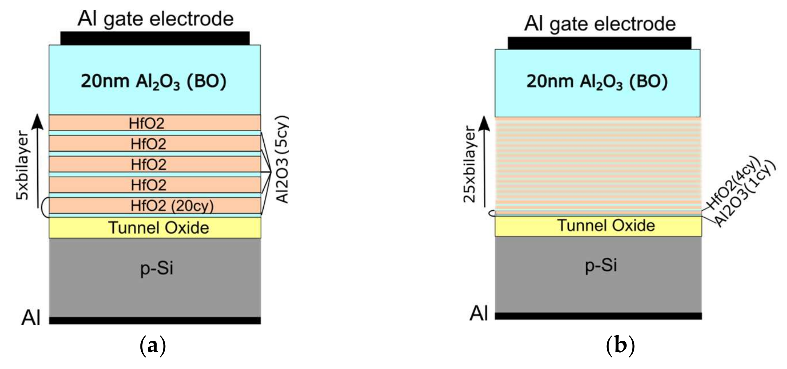
2. Materials and Methods

Metal electrode/blocking oxide (BO)/high-k dielectric/tunnel oxide (TO)/semiconductor (p-Si) (MOHOS) structures were prepared for implementation as a memory cell in charge trapping memory (CTM). The high-k dielectric charge trapping layers were prepared by the thermal atomic layer deposition (ALD) method. Two types of dielectric stacks consisting of HfO2 and Al2O3 were made. The first type of HfO2/Al2O3 stack was constructed by a 5-fold repeating of a HfO2/Al2O3 block composed of a 20 cycles-thick HfO2 sublayer and 5 cycles-thick Al2O3 sublayer (Figure 1a). (The thicknesses of the building sublayers are given by the number of ALD cycles used for deposition, which is a standard practice for this technology.) These structures were briefly assigned as 5 × (20:5). In the second type of HfO2/Al2O3 stack, in order to achieve a doping effect, the structure of the HfO2/Al2O3 block was changed by reducing the thickness of the sublayers—the Al2O3 sublayer was reduced only to 1 cycle, and the HfO2 sublayer was 4 cycles. The number of HfO2/Al2O3 blocks was increased to 25 to ensure equal thickness for both types of HfO2/Al2O3 stacks (structures were briefly assigned as 25 × (4:1)) (Figure 1b). Depositions of HfO2 and Al2O3 were performed at 135 °C by using a tetrakis (dimethylamido) hafnium (TDMA) precursor and trimethylaluminum precursor (TMA), respectively. In both processes, H2O was used as an oxidant and nitrogen was used as a carrier and purging gas between cycles. The deposition of the HfO2/Al2O3 stack was followed by the deposition of a blocking Al2O3 oxide with a thickness of 200 cycles (about 20 nm).
Two types of tunnel oxide were used: (i) SiO2 (with two thicknesses 2.4 or 3.5 nm) grown by a standard thermal oxidation of Si; (ii) Al2O3 layer (about 3 nm thick) deposited under the same ALD conditions as mentioned above. After the deposition of dielectric layers, a part of the structures was subjected to RTA at 800 °C, for 1 min in O2.
The formation of a memory cell in the form of a MIS capacitor was realized by depositing the top and bottom Al electrodes by thermal evaporation. Square top contacts were defined by photolithography.
Nanolaminated Al2O3/HfO2 stacks before and after annealing were subjected to detailed microstructural observations using a TECNAI G2 SuperTWIN FEG (200 kV; Thermo Fisher Scientific Inc., Waltham, MA, USA) transmission electron microscope (TEM). Characterization was carried out in TEM bright-field (TEM BF), high-resolution (HRTEM), as well as scanning-transmission TEM (STEM) modes. Chemical analyses were performed by X-ray energy-dispersive spectroscopy (EDS). Thin foils for TEM analysis were prepared by the focused ion beam (FIB) technique using a QUANTA 200 3D DualBeam microscope (Thermo Fisher Scientific Inc., Waltham, MA, USA). The charge-trapping in the stacks was evaluated by applying square negative and positive voltage pulses of different amplitudes Vp with a duration of 1 s to the top metal electrode (back Al electrode is grounded). Each pulse was followed by a measurement of the C-V curve, and its flat-band voltage, Vfb, shift with respect to the initial C-V curve was determined. The memory windows were defined as the difference between the voltage shifts corresponding to the negative and positive pulses (Supplementary Figure S1). The end values of Vp were defined by the electrical breakdown of capacitors. Retention characteristics were obtained by monitoring the charge loss over time through control C-V measurements after initial charging of the capacitors with a negative or positive charge by applying a voltage pulse Vp = ±27 V, i.e., setting the capacitors to the Program/Erase state. The endurance characteristics were acquired at Vp = ±25 V, and a control C-V curve was recorded after each pulse in order to find the flat-band voltage shift.

3. Results and Discussion

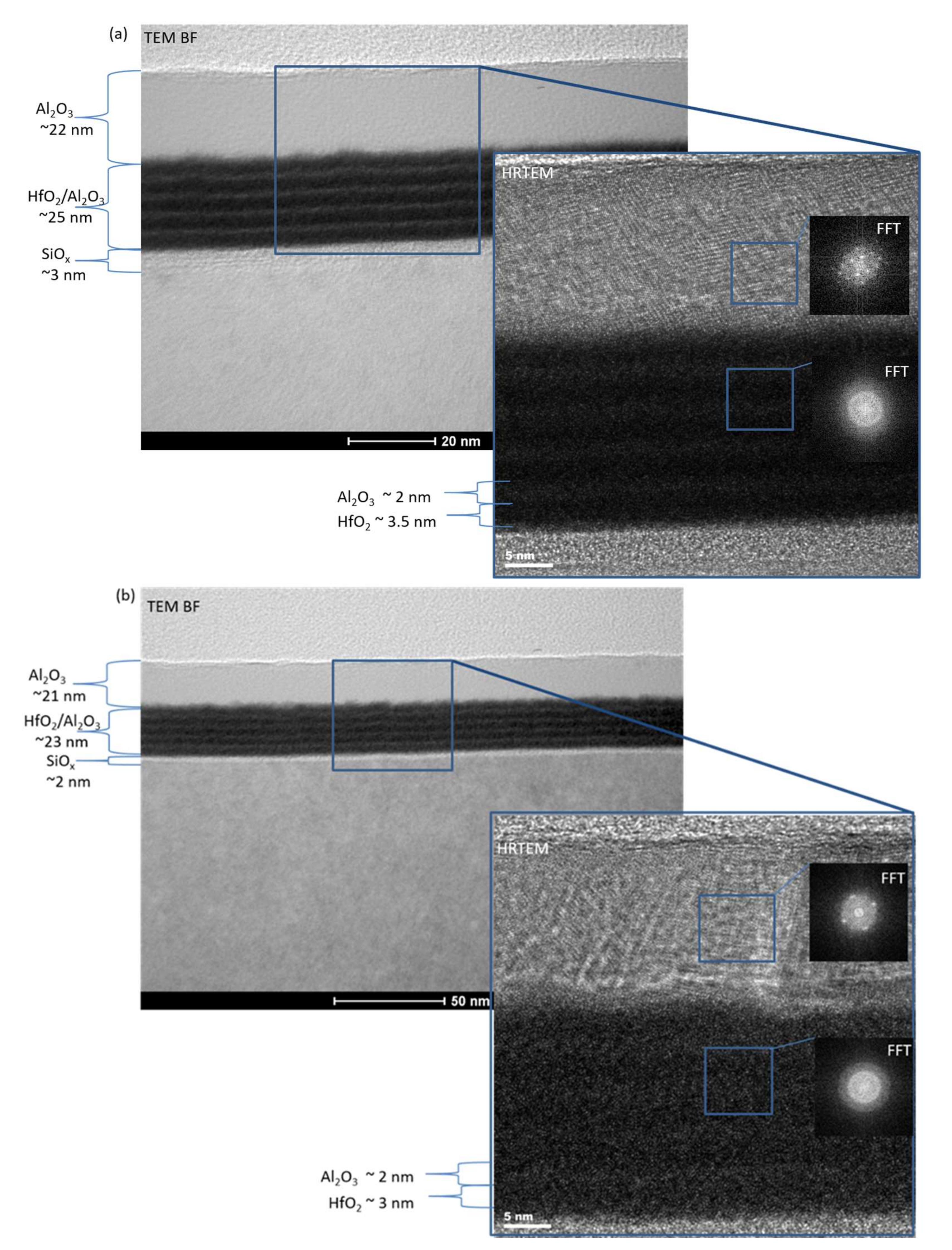
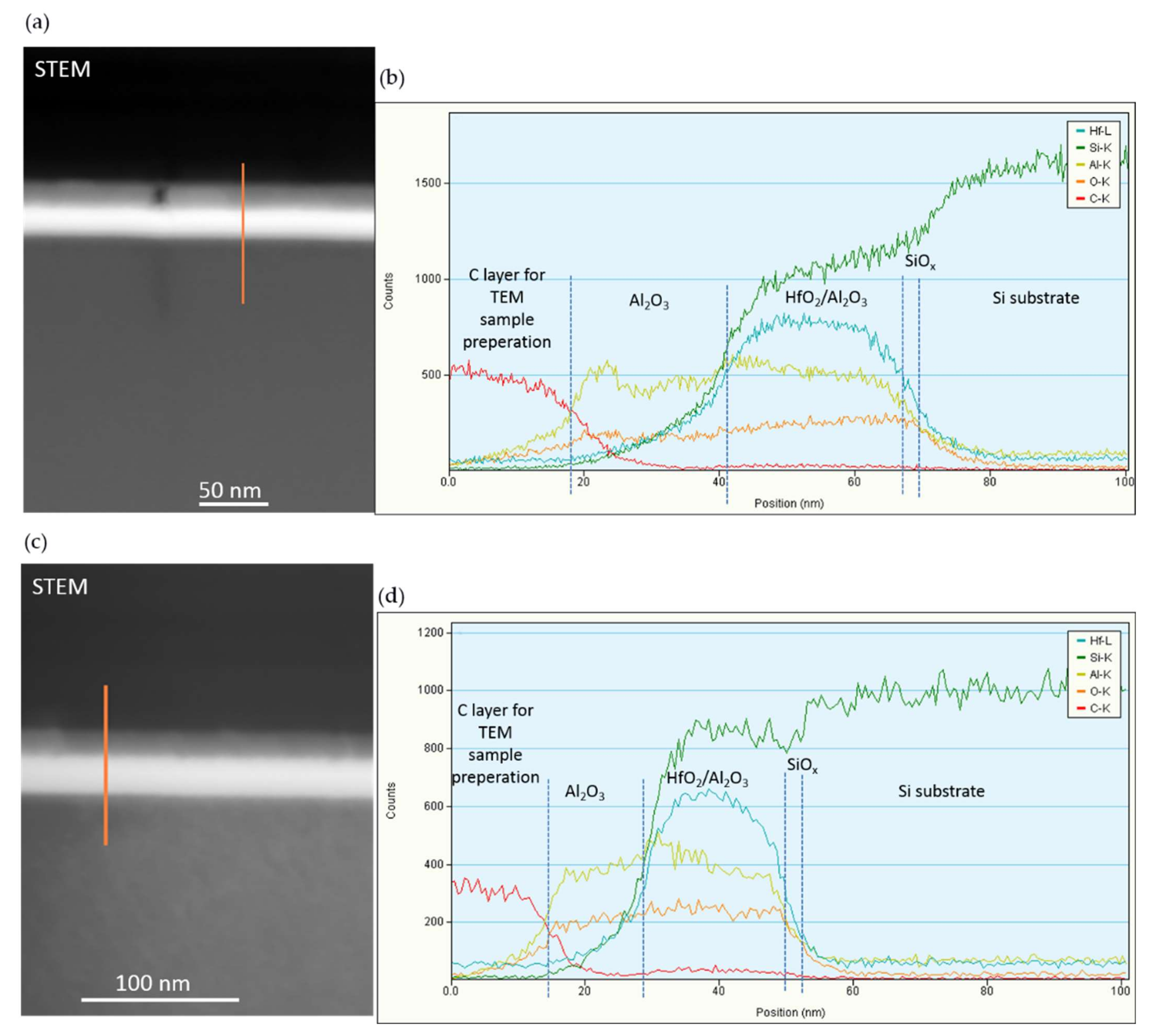
3.1. Transmission Electron Microscopy (TEM)

The TEM observations (Figure 2) show a nanolaminated Al2O3-HfO2 5 × (20:5) stack with SiO2 TO and Al2O3 BO before (Figure 2a) and after annealing (Figure 2b). The analyses confirm the multilayered structure of the Al2O3-HfO2 5 × (20:5) stack. Before annealing, the thicknesses of the individual parts are estimated to be about: 2 nm—SiO2 TO, 25 nm—the HfO2/Al2O3 stack, and 22 nm—the Al2O3 BO (Figure 2a). After RTA, both thicknesses decrease to 23 nm for the HfO2/Al2O3 stack and to 21 nm for Al2O3 BO (Figure 2b), i.e., O2 annealing results in densification of the layers. As is seen, the multilayer structure is maintained after the annealing process, but the HfO2/Al2O3 interfaces are not so sharp as before. Obviously, some intermixing between HfO2 and Al2O3 layers occurs at the interface. This intermixing is very pronounced at the interface with the Al2O3 blocking layer, the roughness of which also increases after RTA. It should be mentioned that HRTEM observations (Figure 2a,b) reveal that crystallization processes of the Al2O3-HfO2 layers do not occur and these layers remain amorphous both before as well as after the high-temperature annealing. The analysis also shows that the Al2O3 BO part both before and after RTA has a crystal structure.
The EDS measurements performed along the line-scan confirm the chemical composition of the HfO2/Al2O3 multilayer structure (Figure 3). The results also show a reduction in the thickness of the Al2O3 BO layer and the HfO2/Al2O3 stack after annealing and the blurring of the HfO2/Al2O3 interfaces, which is evidently visible in the Hf-L distribution diagram. RTA in O2 does not lead to a significant increase in the concentration of oxygen in the structures but improves the homogeneity of its distribution. Another interesting feature is the change in the Si-K profile after RTA associated with the possible diffusion of Si into the HfO2/Al2O3 stack.

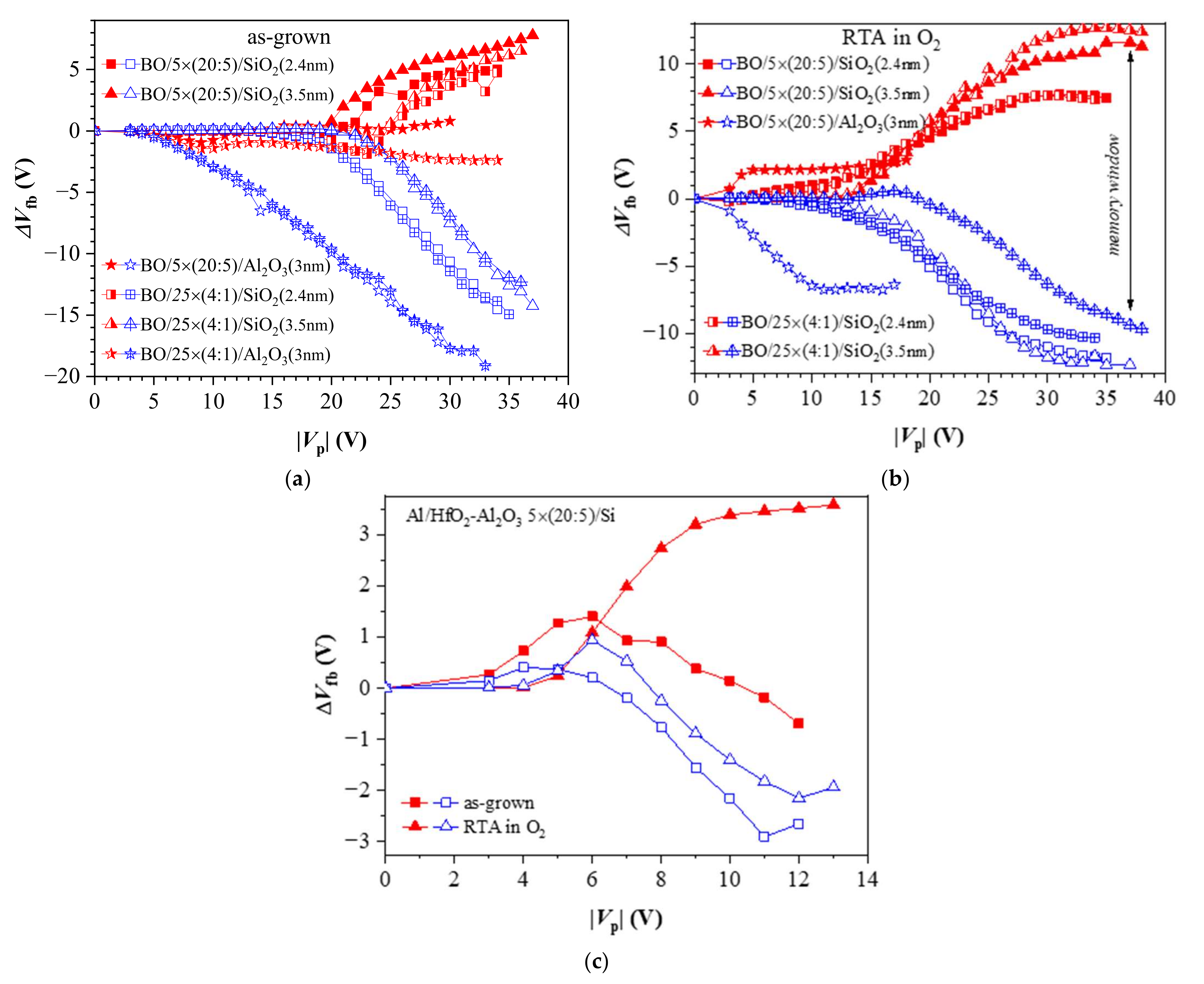
3.2. Charge Trapping Characteristics

Figure 4 compares the charge capture in nanolaminate (5 × (20:5)) and doped (25 × (4:1)) dielectric structures before and after O2 annealing. Before annealing (Figure 4a), the capture of positive charge in samples with Al2O3 TO starts at low Vp~5 V, while for samples with SiO2 TO, this process occurs at substantially larger Vp~16 V for 2.4 nm SiO2 and ~22 V for the 3.5 nm one. The flat-band voltage shift ΔVfb due to positive charge trapping increases progressively (almost linearly) with Vp and it reaches very large values of about 15–20 V with no tendency for saturation. Such a behavior has also been observed for as-deposited stacks without any TO and BO [19] and has been explained with the generation of stress-induced positively charged defects (which is an irreversible process), which adds to the hole trapping (which is a reversible process). The results also reveal that the positive charge trapping is almost the same in samples with the same TO irrespective of the dielectric stack. In other words, it depends on the tunnel oxide (and its thickness) and is weakly affected by the dielectric stack. The last result suggests that the hole capture takes place in traps associated with HfO2. Structures with the thinner SiO2 demonstrate larger hole trapping, which is explained with the larger number of injected charges due to the higher electric field in the thinner layers (at the same applied external voltage) and also to the operating charge transport mechanisms in TO (direct tunneling in the case of 2.4 nm SiO2 and Fowler–Nordheim tunneling for thicker SiO2). However, the capture of electrons depends on the dielectric, as the nanolaminate structures show a stronger electron trapping (respectively, the memory window is larger), which is evidence that this trapping occurs in Al2O3-associated traps. In addition, the electron trapping in nanolaminated stacks starts at lower charging voltages Vp, which allows operation at lower electric fields. It should be noticed that ΔVfb due to negative charge trapping is significantly smaller than that due to positive charge trapping. This could be again explained by the occurrence of two competing process, which give rise to ΔVfb—trapping of electrons in existing traps and the generation of positive charge by high-field electric stress. For structures with Al2O3 TO, regardless of the dielectric layer, the negative charge trapping is very weak, which makes these structures unsuitable as a memory cell in CTM. For this reason, subsequent research is focused on structures with SiO2 as a tunnel oxide.
After O2 annealing, the trapping characteristics change notably (Figure 4b). The capture of electrons in all studied structures increases significantly compared to the negative charge trapping before RTA. This capture is similar for the stacks of the same SiO2 thickness and is only slightly affected by the type of dielectric stack. Compared to the stacks before annealing, the positive charge trapping decreases and exhibits a saturation at a higher Vp. This behavior implies that, after RTA in O2, the stacks are more resistant to high-electric-field degradation and no positive charge is generated. As a result, the net positive charge trapping decreases and the net negative charge trapping increases. A similar effect is also observed in the nanolaminated stack without any TO and BO (Figure 4c), as well as in stacks with various HfO2/Al2O3 ratios without BO and TO [19]. This is most likely the reason why the two branches of the trapping characteristics become more symmetrical. In contrast to pre-annealing structures where hole trapping does not depend on CTL (nanolaminate or doped stack) (Figure 4a), after RTA, the hole trapping is stronger in nanolaminate structures (Figure 4b). The electron and hole trappings start at lower Vp compared to as-deposited stacks, which means lower operation voltages. It should be noted that the nanolaminated 5 × (20:5) stack with Al2O3 TO exhibits an increase in negative charge trapping and a significant memory window (about 9 V at Vp > 10 V) forms. However, the positive and negative charge trappings are strongly asymmetric, and a major part of the memory window (about 7 V) is due to positive charge trapping. The doped 25 × (5:1) stack with Al2O3 TO does not show any charge trapping (neither positive nor negative) after RTA and thus is not shown in Figure 4b.
The density of trapped electrons and holes was estimated using its relation to ΔVfb [28]:
Δ V f b = q ρ X T ε B O d B O + ε B O X T 2 ε T
where ρ is the spatial density of the trapped charge, q is the charge of the electron, εBO is the dielectric constant of BO, dBO is the thickness of BO, and XT and εT are the thickness and dielectric constant of the charge trapping layer, respectively. ρ for electrons and holes is evaluated only for the annealed samples, as the observed saturation of ΔVfb at high Vp suggests that all available traps are filled, so ρ represents the density of the traps. The obtained values are presented in Table 1.

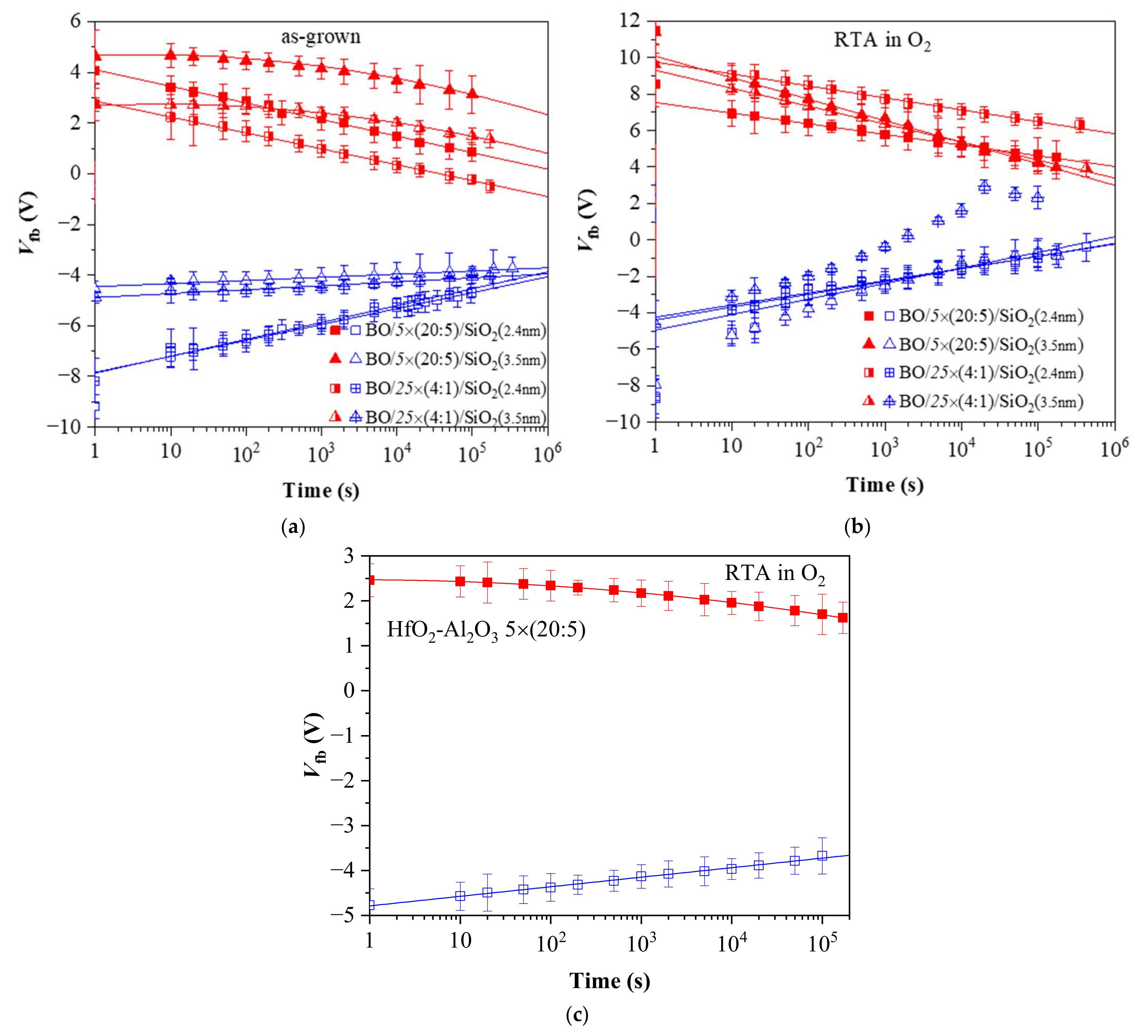
3.3. Retention Characteristics

3.3.1. Structures before O2 Annealing

The retention characteristics measured after a pulse voltage of Vp = 27 V for structures before and after O2 annealing are presented in Figure 5. The results show that the retention characteristics of holes for the 5 × (20:5) and 25 × (4:1) structures before RTA almost coincide for the same thickness of the tunnel SiO2 (Figure 5a), i.e., the retention of holes in the structures depends on the TO thickness and is almost independent of the dielectric stack (nanolaminate structure or doped oxide). The retention characteristics also confirm the stronger positive charge trapping in structures with a thinner 2.4 nm SiO2 irrespective of the dielectric layer. The discharge of trapped holes follows a linear law in the log(t) scale, which is consistent with the trap-to-band tunneling mechanism (from the trap level in high-k stack through the SiO2 layer to the Si valence band). For this detrapping process, the time constant of the hole is given as τ0∙exp(αTOdTO)exp(αhigh-kX), where τ0 is a constant for the traps; dTO is the thickness of TO; X is the trap distance from TO (tunneling distance); αTO and αhigh-k are coefficients dependent on trap energy and band offsets [29]. As can be seen, the observed discharge rate is higher for stacks with thinner SiO2 that correlates with the higher probability of back-tunneling of charge carriers in this case.
The discharge rate of holes through 3.5 nm SiO2 is very low, i.e., SiO2 of such a thickness provides a good barrier to back-tunneling of holes. Neither charge trapping nor the discharge mechanism and rate depend on the dielectric stack—nanolaminated HfO2/Al2O3 or Al-doped HfO2. These results imply that the hole trapping in the two kinds of stacks occurs in the same type of traps, i.e., these traps most likely are related to HfO2. The tunneling SiO2 layer dominates the retention characteristics of holes (discharge rate) by spatially shifting the traps position further from Si and forming an additional potential barrier.
Figure 5a also confirms the stronger electron trapping in the HfO2/Al2O3 multilayer structures compared to Al-doped HfO2 ones. In the case of electrons as well as holes, the discharge rate is higher for structures with a thinner tunnel SiO2 and it is evident that electron detrapping follows different discharge laws for the samples with 2.4 and 3.5 nm SiO2. For capacitors with a 2.4 nm tunnel SiO2, the Vfb dependence is linear in the log(t) scale, i.e., the electron discharge performs through the trap-to-band tunneling mechanism. It should be noted that the straight lines for the 5 × (20:5) and 25 × (4:1) stacks are parallel, which implies the same discharge mechanism for both stacks. For structures with a 3.5 nm tunnel SiO2, the Vfb dependence on log(t) is more complicated in the case of electron discharge, which suggests that either the mechanism of electron loss is different or several mechanisms operate in parallel. More specifically, the voltage decay is well fitted by the ln2(t) dependence, indicating that the electron detrapping most likely occurs via the Poole–Frenkel mechanism [19,30]. Therefore, for a stored negative charge, field-assisted thermal excitation of the trapped electrons takes place and appends to the charge loss determined by tunneling. As the contribution of PF emission is not clearly observed for the trapped holes, we could suggest that hole traps are much deeper than the electron ones. This could be qualitatively inferred from the fact that for a given electric field distribution in the stack (i.e., distribution of the trapped charge), the electric-field-induced barrier lowering is the same for all kind of traps. However, in case of deep traps, this lowering is not enough for sizable thermal excitation of the trapped carriers at room temperature, i.e., for PF emission. For the shallow enough traps, on the other hand, the electric field provides enough barrier reduction so that carriers could be readily emitted to the corresponding band at room temperature; hence, the PF mechanism is observed. It should also be noted that the shape of the Vfb vs. log(t) dependence could also reflect the spatial and energy distribution of the traps. In any case, however, different Vfb vs. log(t) dependencies for trapped electrons and holes support the assumption that the origin of these centers is different. The electron discharge in stacks with 3.5 nm SiO2 does not depend on the type of dielectric stack as well, as the curves for the two dielectrics are parallel to each other. These results allow the conclusion that electron traps in the two kinds of stacks have the same origin, but their density is higher in multilayered 5 × (20:5) stacks.

3.3.2. Structures after O2 Annealing

After O2 annealing, significant changes occur not only in the number of trapped charges (electrons or holes), but also in the discharge characteristics and their dependence on the parameters of the structure (thickness of TO and the type of dielectric stack) (Figure 5b). For samples with a thinner 2.4 nm SiO2 TO, despite the stronger electron trapping and weaker hole trapping after O2 annealing, the discharge rates of both types of charges are similar to those in the structures before O2 annealing. In other words, oxygen annealing changes the density of the trapped charge, but does not alter their discharge mechanism in stacks with 2.4 nm SiO2.
Contrary to expectations, the electron discharge rate is higher in structures with a thicker 3.5 nm SiO2 compared to stacks with a thinner 2.4 nm SiO2 and slightly depends on the dielectric stack. This result is unexpected and shows that the annealing most likely results in a reaction between SiO2 and the dielectric, which leads to the formation of traps in the TO, through which the stored charge is discharged. The discharge rate of the trapped holes is also higher than that in the structures before O2 annealing, with the highest being for doped layers (25 × (5:1)) on thicker SiO2. These results show that although O2 annealing leads to strong electron trapping in the dielectric layer, it is not suitable for structures with TO and BO, as it generates defects (most likely due to the interaction between the HfO2/Al2O3 charge trapping layer and TO), which cause a faster discharge of the charges stored in the structures. This finding is in line with reports of other authors [31] that high-temperature annealing deteriorates the retention properties of tunneling oxide. Further, as it might be inferred from Figure 5b, the discharge rate within first 10 s of the annealed stacks is noticeably higher than that of the corresponding as-grown structures, which also agrees well with the suggested defect generation in TO and the high-k/TO interface during the annealing. This conclusion is additionally supported by the retention characteristics of the O2-annealed multilayered 5 × (20:5) stacks without any intentionally grown TO and BO (Figure 5c). As is seen, the hole discharge follows a linear law, while electron discharge is well fitted by ln2(t), i.e., the retention in these stacks is very similar to the retention in stacks with a thicker SiO2 TO and BO before annealing (Figure 5a).

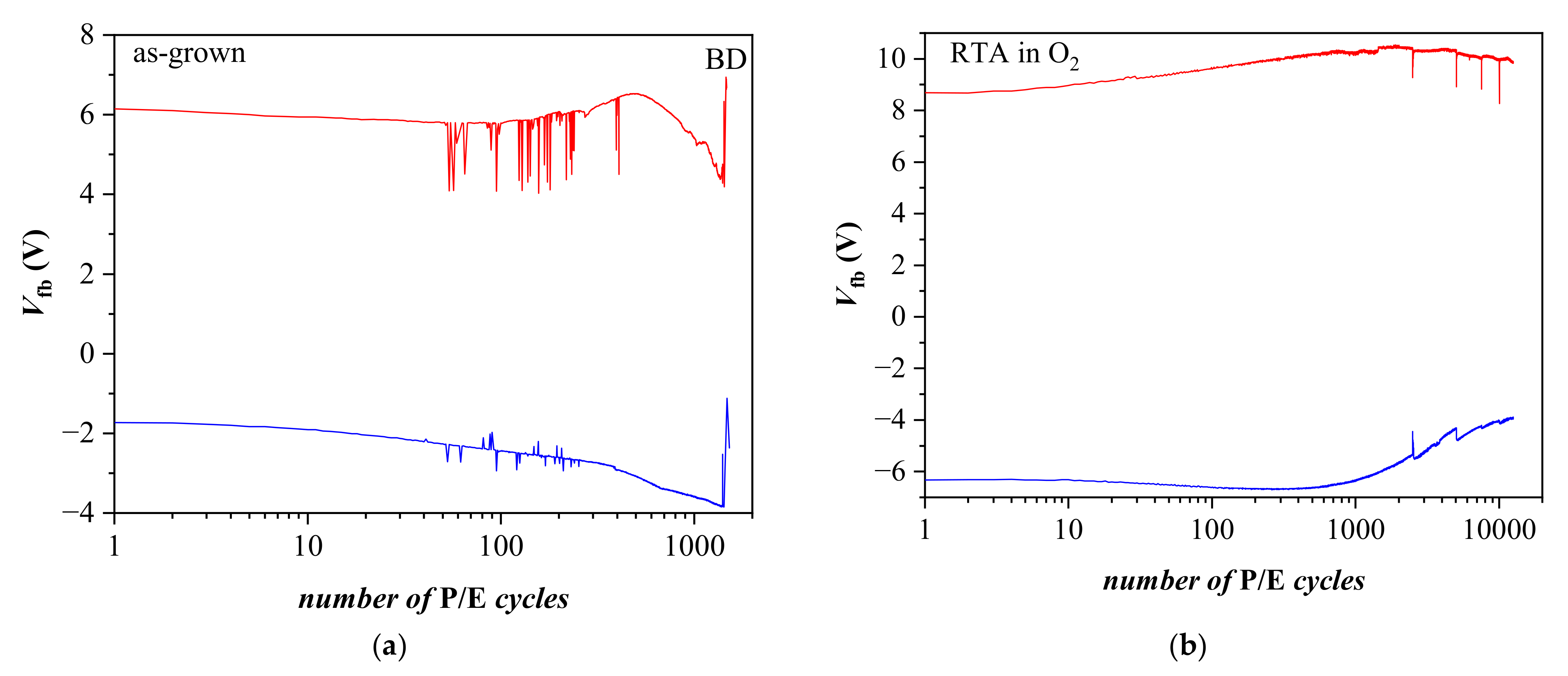
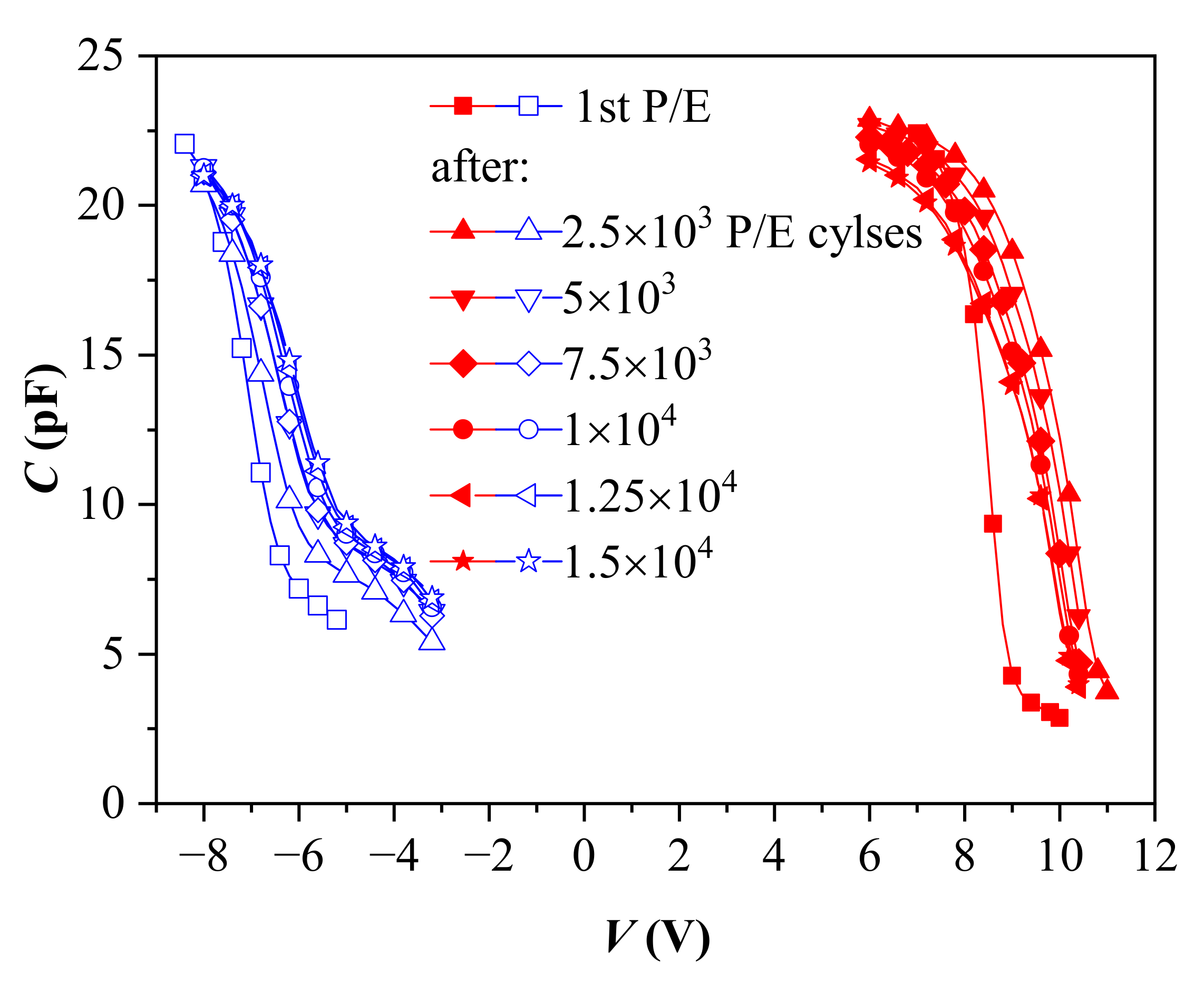
3.4. Endurance Characteristics

The endurance characteristics measured at pulse voltage Vp = ±25 V of as-deposited and annealed nanolaminated HfO2/Al2O3 stacks with 3.5 nm SiO2 TO are shown in Figure 6. During the first several hundred program/erase (P/E) cycles, the as-deposited structure (Figure 6a) reveals some instabilities, especially in electron trapping, which tend to recover. However, after about 600 P/E cycles, substantial degradation in both positive and negative charge trapping is observed, with a stable tendency to increase positive charge trapping and decrease negative charge trapping. Such a behavior could be explained by the progressive accumulation of positive charge generated by the high electric field, i.e., it is fully consistent with the trapping characteristics in Figure 4a. It should be mentioned that the annealed samples reveal better endurance than as-deposited ones. As is seen in Figure 6, the former structures can withstand more than 104 P/E cycles without coming to breakdown, while the as-deposited structures are broken-down shortly after 1000 P/E cycles. In addition, the endurance characteristics of the annealed sample are qualitatively different, and the structure exhibits a more stable behavior (Figure 6b). Both electron and hole trapping increase gradually up to about 1000 P/E cycles. The degradation of the endurance characteristics is observed for a larger number (>1000) of P/E cycles. Vfb related both to electron and hole trapping decreases gradually as the number of P/E cycles exceeds 1000. The decrease related to positive charge trapping is stronger. Despite the decrease, the Vfb related to electron trapping at about 1.5 × 10⁴ P/E cycles is still larger than that in the first P/E cycle. The evolution of the C-V curves with an increasing number of P/E cycles (Figure 7) gives evidence for a possible reason of the endurance degradation of annealed stacks.
The slope of the C-V curves changes with the P/E cycles, which reveals the interface states generation. These are most probably traps close to the valence band edge, which allow trapped holes to be easily discharged. Figure 7 also demonstrates that after positive charging of the capacitors (under −Vp), some severe changes in the control C-V curve shape occur, which are not observed with electron injection (+Vp). In the positively charged state, the region of the C-V curve corresponding to the transition from the flat band to inversion is characterized by a low slope. As this slanting section is not observed in the curves after electron injection, its origin is most probably not related to the interface states at the TO/Si interface. Although further investigation is required, we could suggest that this behavior is due to positive charge leakage through annealing defects in both BO and TO layers. As mentioned above, the interaction of the high-k stack with TO and BO during the RTA (evidenced by TEM) could be the reason for the deterioration of retention characteristics.
For illustration, Figure 8 demonstrates band diagrams of investigated capacitors with trapped positive (V = −4 V) and negative (V = 10.5 V) charge, respectively. Band diagrams are obtained with the Multi-Dielectric Energy Band Diagram Program [32]. In the case of positive trapped charge in weak and strong inversion (Figure 8a), some of the trapped holes could be lost by tunneling through TO facilitated by defect sites (denoted by x in Figure 8) either in the bulk of TO or at its interfaces with Si and high-k stack. Additionally, the positive trapped charge could also be decreased by the tunneling of electrons from the inversion layer via defect sites in TO into the HfO2-Al2O3 stack. When the trapped charge is negative, under inversion conditions, the tunneling electrons from Si will compensate the charge leakage toward the Al gate (Figure 8b); the tunneling of holes into the CT stack is hampered by their low density in the Si surface region.

4. Conclusions

The results presented in this work reveal that the charge trapping and storage in the metal/blocking oxide/high-k charge trapping layer/tunnel oxide/Si (MOHOS) structures with HfO2/Al2O3-based CTL are strong functions of the stack parameters (composition of CTL; type of tunneling oxide; thickness) as well as annealing steps. Electron trapping in HfO2/Al2O3 nanolaminate stacks is stronger compared to Al-doped HfO2 layers, while neither the retention of electrons, nor their discharge mechanism and discharge rate depend on the CTL. These results imply that electron trapping in both types of CTL occurs in the same type of traps, the density of which is higher in the HfO2/Al2O3 nanolaminate, and gives us a reason to conclude that these traps are related to Al2O3. On the other hand, hole trapping does not depend on the CTL; hence, it is related to HfO2 traps. The retention of both electrons and holes is most strongly affected by the tunneling oxide and its thickness. The 3.5 nm SiO2 provides a good barrier to back-tunneling of trapped charges. The as-deposited HfO2/Al2O3-based CTLs are vulnerable to high electric field stress, which generates a positive charge and deteriorates their endurance characteristics. The post-deposition O2 annealing significantly increases the electron trapping in the stacks and improves their susceptibility to high electric field stress, which manifests as wider memory windows and better endurance characteristics. However, high-temperature annealing deteriorates the retention of stored charges, which is most likely due to defects generation in the tunneling oxide as a result of the interfacial reaction between CTL and TO. Al2O3 deposited by ALD at low temperature is not suitable for the tunneling oxide. The results presented could help in a rational approach toward engineering of MOHOS structures to be implemented in flash NVM memories.

Supplementary Materials

The following supporting information can be downloaded at: https://www.mdpi.com/article/10.3390/ma15186285/s1, Figure S1: An illustration of the memory window definition.

Author Contributions

Conceptualization, A.P. and D.S.; formal analysis, D.S. and A.P.; investigation, T.S., T.I., J.W.-B. and M.J.-S.; resources, E.G., T.I. and W.W.; writing—original draft preparation, A.P. and D.S.; writing—review and editing, E.G. and J.W.-B.; visualization, D.S.; project administration, D.S.; funding acquisition, D.S. and A.P. All authors have read and agreed to the published version of the manuscript.

Funding

This research was funded by the Bulgarian National Scientific Fund, Project KP-06-H37/32.

Institutional Review Board Statement

Not applicable.

Informed Consent Statement

Not applicable.

Data Availability Statement

Not applicable.

Conflicts of Interest

The authors declare no conflict of interest.

References

  1. Yoshimitsu, Y.; Yoshinari, K.; Toshimasa, M. Scalable Virtual-Ground Multilevel-Cell Floating-Gate Flash Memory. IEEE Trans. Electron Devices 2013, 60, 2518–2524. [Google Scholar]
  2. Goda, A. Recent Progress on 3D NAND Flash Technologies. Electronics 2021, 10, 3156. [Google Scholar] [CrossRef]
  3. Dimitrakis, P. Charge-Trapping Non-Volatile Memories; Dimitrakis, P., Ed.; Springer: Cham, Switzerland, 2015. [Google Scholar]
  4. Zhao, C.; Zhao, C.Z.; Taylor, S.; Chalker, P.R. Review on Non-Volatile Memory with High-k Dielectrics: Flash for Generation Beyond 32 nm. Materials 2014, 7, 5117–5145. [Google Scholar] [CrossRef]
  5. Park, G.H.; Cho, W.J. Reliability of modified tunneling barriers for high performance nonvolatile charge trap flash memory application. Appl. Phys. Lett. 2010, 96, 043503. [Google Scholar] [CrossRef]
  6. Hwang, C.S. Prospective of Semiconductor Memory Devices: From Memory System to Materials. Adv. Electron. Mater. 2015, 1, 1400056. [Google Scholar] [CrossRef]
  7. Bu, J.; White, M. Design Considerations in Scaled SONOS Nonvolatile Memory Devices. Solid-State Electron. 2001, 45, 113–120. [Google Scholar] [CrossRef]
  8. Chau, R.; Doyle, B.; Datta, S.; Kavalieros, J.; Zhang, K. Integrated Nanoelectronics for the Future. Nat. Mater. 2007, 6, 810–812. [Google Scholar] [CrossRef] [PubMed]
  9. She, M.; Takeuchi, H.; King, T.-J. Improved SONOS-type flash memory using HfO2 as trapping layer. In Proceedings of the IEEE Nonvolatile Semiconductor Memory Workshop, Monterey, CA, USA, 16–20 February 2003; pp. 53–55. [Google Scholar]
  10. Lee, K.H.; Lin, H.-C.; Huang, T.-Y. Novel gate-all-around polycrystalline silicon nanowire memory device with HfAlO charge-trapping layer. Jpn. J. Appl. Phys. 2013, 53, 014001. [Google Scholar] [CrossRef]
  11. You, H.W.; Cho, W.J. Charge trapping properties of the HfO2 layer with various thicknesses for charge trap flash memory applications. Appl. Phys. Lett. 2010, 96, 093506. [Google Scholar] [CrossRef]
  12. Zhu, C.; Huo, Z.; Xu, Z.; Zhang, M.; Wang, Q.; Liu, J.; Long, S.; Liu, M. Performance enhancement of multilevel cell nonvolatile memory by using a bandgap engineered high-k, trapping layer. Appl. Phys. Lett. 2010, 97, 253503. [Google Scholar] [CrossRef]
  13. Lan, X.; Ou, X.; Cao, Y.; Tang, S.; Gong, C.; Xu, B.; Xia, Y.; Yin, J.; Li, A.; Yan, F.; et al. The effect of thermal treatment induced inter-diffusion at the interfaces on the charge trapping performance of HfO2/Al2O3 nanolaminate- based memory devices. J. Appl. Phys. 2013, 114, 044104. [Google Scholar] [CrossRef]
  14. Paskaleva, A.; Rommel, M.; Hutzler, A.; Spassov, D.; Bauer, A.J. Tailoring the electrical properties of HfO2 MOS-devices by aluminum doping. ACS Appl. Mater. Interfaces 2015, 7, 17032–17043. [Google Scholar] [CrossRef] [PubMed]
  15. Cui, Z.; Xin, D.; Kim, T.; Choi, J.; Cho, J.; Yi, J. Improvement of the Charge Retention of a Non-Volatile memory by a Bandgap-Engineered Charge Trap Layer. ECS J. Solid State Sci. Technol. 2021, 10, 125002. [Google Scholar] [CrossRef]
  16. Hou, X.; Yan, X.; Liu, C.; Ding, S.; Zhang, D.W.; Zhou, P. Operation mode switchable charge-trap memory based on few-layer MoS2. Semicond. Sci. Technol. 2018, 33, 034001. [Google Scholar] [CrossRef]
  17. Spiga, S.; Driussi, F.; Lamperti, A.; Congedo, G.; Salicio, O. Effects of Thermal Treatments on the Trapping Properties of HfO2 Films for Charge Trap Memories. Appl. Phys. Express 2012, 5, 021102. [Google Scholar] [CrossRef]
  18. Kim, J.; Kim, J.; Cho, E.C.; Yi, J. Analysis of HfO2 Charge Trapping Layer Characteristics After UV Treatment. ECS J. Solid State Sci. Technol. 2021, 10, 044003. [Google Scholar] [CrossRef]
  19. Spassov, D.; Paskaleva, A.; Krajewski, T.A.; Guziewicz, E.; Luka, G.; Ivanov, T. Al2O3/HfO2 Multilayer High-k Dielectric Stacks for Charge Trapping Flash Memories. Phys. Status Solidi A 2018, 215, 1700854. [Google Scholar] [CrossRef]
  20. Spassov, D.; Paskaleva, A.; Krajewski, T.A.; Guziewicz, E.; Luka, G. Hole and electron trapping in HfO2/Al2O3 nanolaminated stacks for emerging non-volatile flash memories. Nanotechnology 2018, 29, 505206. [Google Scholar] [CrossRef]
  21. Spassov, D.; Paskaleva, A.; Krajewski, T.A.; Guziewicz, E.; Ivanov, T. Leakage currents in Al2O3/HfO2 multilayer high-k stacks and their modification by post-deposition annealing steps. J. Phys. Conf. Ser. 2019, 1186, 012025. [Google Scholar] [CrossRef]
  22. Spassov, D.; Paskaleva, A.; Guziewicz, E.; Davidović, V.; Srboljub, S.; Djorić-Veljković, S.; Ivanov, T.; Stanchev, T.; Stojadinović, N. Radiation Tolerance and Charge Trapping Enhancement of ALD HfO2/Al2O3 Nanolaminated Dielectrics. Materials 2021, 14, 849. [Google Scholar] [CrossRef]
  23. Robertson, J.; Wallace, R.M. High-K materials and metal gates for CMOS applications. Mater. Sci. Eng. R Rep. 2015, 88, 1–41. [Google Scholar] [CrossRef] [Green Version]
  24. Lee, C.H.; Hur, S.H.; Shin, Y.C.; Choi, J.H.; Park, D.G.; Kim, K. Charge-trapping device structure of SiO2∕SiN∕high-k dielectric Al2O3 for high-density flash memory. Appl. Phys. Lett. 2005, 86, 152908. [Google Scholar] [CrossRef]
  25. Seo, Y.J.; Kim, K.C.; Kim, H.D.; Joo, M.S.; An, H.M.; Kim, T.G. Correlation between charge trap distribution and memory characteristics in metal/oxide/nitride/oxide/silicon devices with two different blocking oxides, Al2O3 and SiO2. Appl. Phys. Lett. 2008, 93, 063508. [Google Scholar] [CrossRef]
  26. Hou, Z.; Wu, Z.; Yin, H. Performance Enhancement for Charge Trapping Memory by Using Al2O3/HfO2/Al2O3Tri-Layer High-κ Dielectrics and High Work Function Metal Gate. ECS J. Solid State Sci. Technol. 2018, 7, N91–N95. [Google Scholar] [CrossRef]
  27. Agrawal, K.; Yoon, G.; Kim, J.; Chavan, G.; Kim, J.; Park, J.; Phong, P.; Cho, E.; Yi, J. Improving Retention Properties of ALD-AlxOy Charge Trapping Layer for Non-volatile Memory application. ECS J. Solid State Sci. Technol. 2020, 9, 043002. [Google Scholar] [CrossRef]
  28. Kim, T.H.; Park, I.H.; Lee, J.D.; Shin, H.C.; Park, B.G. Electron trap density distribution of Si-rich silicon nitride extracted using the modified negative charge decay model of silicon-oxide-nitride-oxide-silicon structure at elevated temperatures. Appl. Phys Lett. 2006, 89, 063508. [Google Scholar] [CrossRef]
  29. Lundkvist, L.; Lundstrom, I.; Svensson, C. Discharge of MNOS structures. Solid State Electron. 1973, 16, 811–823. [Google Scholar] [CrossRef]
  30. Lehovec, K.; Fedotowsky, A. Charge retention of MNOS devices limited by Frenkel-Poole detrapping. Appl. Phys. Lett. 1978, 32, 335–338. [Google Scholar] [CrossRef]
  31. Arreghini, A.; Zahid, M.B.; Van den bosch, G.; Suhane, A.; Breuil, L.; Cacciato, A.; Van Houdt, J. Effect of high temperature annealing on tunnel oxide properties in TANOS devices. Microelectron. Eng. 2011, 88, 1155–1158. [Google Scholar] [CrossRef]
  32. Southwick III, R.G.; Sup, A.; Jain, A.; Knowlton, W.B. Interactive Simulation Tool for Complex Multilayer Dielectric Devices. IEEE Trans. Device Mater. Reliab. 2011, 11, 236–243. [Google Scholar] [CrossRef]
Figure 1. Schematic presentation of the memory capacitors with: (a) nanolaminated and (b) doped charge trapping layer.
Materials 15 06285 g001
Figure 2. TEM characterization of nanolaminate 5 × (20:5) HfO2/Al2O3 high-k dielectric stack with 2.4 nm SiO2 and BO (Al2O3) before (a) and after O2 annealing (b).
Materials 15 06285 g002
Figure 3. Qualitative chemical analysis (EDS) of nanolaminate 5 × (20:5) HfO2—Al2O3 layers with 2.4 nm SiO2 and BO (Al2O3); STEM images after (a) and before annealing (c) with marked line-scan; diagrams of the elements distributions (bd) recorded along marked line-scan.
Materials 15 06285 g003
Figure 4. The flat band voltage shifts as a function of voltage pulse amplitude: (a) as-grown stacks; (b) after O2 annealing; (c) 5 × (20:5) HfO2/Al2O3 stack without any TO and BO. Red closed symbols correspond to +Vp and the blue open symbols to –Vp.
Materials 15 06285 g004
Figure 5. Charge retention characteristics in capacitors with various HfO2-Al2O3 stacks: (a) before and (b) after RTA in O2; (c) HfO2-Al2O3 5 × (20:5) stack without BO and TO after RTA. The filled red symbols correspond to a negative charge (respectively, positive values of Vfb) and the open blue ones correspond to a positive charge (negative values of Vfb).
Materials 15 06285 g005
Figure 6. Endurance of BO/5 × (20:5)/TO (3.5 nm SiO2) capacitors before (a) and after O2 annealing (b) measured under voltage pulses +/−25 V. Red lines correspond to Vp = 25 V, blue ones to Vp = −25 V.
Materials 15 06285 g006
Figure 7. C-V curves during the endurance measurements with ±25 V voltage pulses.
Materials 15 06285 g007
Figure 8. Band diagrams of capacitor with 3.5 nm SiO2 TO layer with positive trapped charge at applied voltage of −4 V (a), and (b) with negative trapped charge at V = 10.5 V. The trapped charge is roughly equal to the stored charges in the capacitor presented in Figure 7.
Materials 15 06285 g008
Table 1. Spatial density of trapped electrons, ρe, and holes, ρh, for the structures annealed in O2.
Structure Typeρe (cm−3)ρh (cm−3)
BO/5 × (20:5)/2.4 nm SiO29.59 × 10181.48 × 1019
BO/5 × (20:5)/3.5 nm SiO21.45 × 10191.54 × 1019
BO/5 × (20:5)/3 nm Al2O33.60 × 10188.00 × 1018
BO/25 × (4:1)/2.4 nm SiO29.52 × 10181.29 × 1019
BO/25 × (4:1)/3.5 nm SiO21.58 × 10191.21 × 1019
Publisher’s Note: MDPI stays neutral with regard to jurisdictional claims in published maps and institutional affiliations.

