
Raytracing Modelling of Infrared Light Management Using Molybdenum Disulfide (MoS2) as a Back-Reflector Layer in a Silicon Heterojunction Solar Cell (SHJ)

 ,
,  , , , , , ,
Abstract
:1. Introduction
2. Methodology
3. Results
3.1. Photo-Current Density Simulation
3.2. EQE Profile
4. Conclusions
Author Contributions
Funding
Acknowledgments
Conflicts of Interest
References
- VDMA ITRPV Results 2021. Available online: https://itrpv.vdma.org/documents/27094228/29066965/Readiness0ITRPV02020/2a8588fd-3ac2-d21d-2f83-b8f96be03e51 (accessed on 14 July 2021).
- Elsmani, M.I.; Fatima, N.; Jallorina, M.P.A.; Sepeai, S.; Su’ait, M.S.; Ludin, N.A.; Teridi, M.A.M.; Sopian, K.; Ibrahim, M.A. Recent Issues and Configuration Factors in Perovskite-Silicon Tandem Solar Cells towards Large Scaling Production. Nanomaterials 2021, 11, 3186. [Google Scholar] [CrossRef] [PubMed]
- Green, M.A.; Dunlop, E.D.; Hohl-Ebinger, J.; Yoshita, M.; Kopidakis, N.; Hao, X. Solar cell efficiency tables (Version 58). Prog. Photovolt. Res. Appl. 2021, 29, 657–667. [Google Scholar] [CrossRef]
- Green, M.A.; Dunlop, E.D.; Hohl-Ebinger, J.; Yoshita, M.; Kopidakis, N.; Hao, X. Solar cell efficiency tables (version 59). Prog. Photovolt. Res. Appl. 2022, 30, 3–12. [Google Scholar] [CrossRef]
- Nasir, N.S.M.; Sepeai, S.; Leong, C.S.; Sopian, K.; Zaidi, S.H. Infra-red investigation on silicon solar cells. Malays. J. Anal. Sci. 2017, 21, 1134–1142. [Google Scholar] [CrossRef]
- Miller, O.D.; Yablonovitch, E.; Kurtz, S.R. Strong internal and external luminescence as solar cells approach the Shockley-Queisser limit. IEEE J. Photovolt. 2012, 2, 303–311. [Google Scholar] [CrossRef] [Green Version]
- Andreani, L.C.; Bozzola, A.; Kowalczewski, P.; Liscidini, M.; Redorici, L. Silicon solar cells: Toward the efficiency limits. Adv. Phys. X 2019, 4, 1548305. [Google Scholar] [CrossRef] [Green Version]
- Pfeffer, F.; Eisenlohr, J.; Basch, A.; Hermle, M.; Lee, B.G.; Goldschmidt, J.C. Systematic analysis of diffuse rear reflectors for enhanced light trapping in silicon solar cells. Sol. Energy Mater. Sol. Cells 2016, 152, 80–86. [Google Scholar] [CrossRef]
- Barugkin, C.; Paetzold, U.W.; Catchpole, K.R.; Basch, A.; Carius, R. Highly Reflective Dielectric Back Reflector for Improved Efficiency of Tandem Thin-Film Solar Cells. Int. J. Photoenergy 2016, 2016, 7390974. [Google Scholar] [CrossRef] [Green Version]
- Moulin, E.; Wilhelm Paetzold, U.; Siekmann, H.; Worbs, J.; Bauer, A.; Carius, R. Study of thin-film silicon solar cell back reflectors and potential of detached reflectors. Energy Procedia 2011, 10, 106–110. [Google Scholar] [CrossRef] [Green Version]
- Chavali, R.V.K.; De Wolf, S.; Alam, M.A. Device physics underlying silicon heterojunction and passivating-contact solar cells: A topical review. Prog. Photovolt. Res. Appl. 2018, 26, 241–260. [Google Scholar] [CrossRef]
- Razzaq, A.; Allen, T.G.; Liu, W.; Liu, Z.; De Wolf, S. Silicon heterojunction solar cells: Techno-economic assessment and opportunities. Joule 2022, 6, 514–542. [Google Scholar] [CrossRef]
- Holman, Z.C.; Filipič, M.; Descoeudres, A.; De Wolf, S.; Smole, F.; Topič, M.; Ballif, C. Infrared light management in high-efficiency silicon heterojunction and rear-passivated solar cells. J. Appl. Phys. 2013, 113, 013107. [Google Scholar] [CrossRef] [Green Version]
- Dittrich, T. Materials Concepts for Solar Cells, 2nd ed.; World Scientific: Singapore, 2018; pp. 1–535. [Google Scholar] [CrossRef] [Green Version]
- Mehdi, L.; Goodnick, S.M.; Goryll, M.; Bertoni, M.; Bowden, S.; Stuckelberger, M. Fill Factor Loss Mechanisms: Analysis and Basic Understanding in Silicon Hetero-Junction Solar Cells; Arizona State University: Tempe, AZ, USA, 2018. [Google Scholar]
- Bush, K.A.; Palmstrom, A.F.; Yu, Z.J.; Boccard, M.; Cheacharoen, R.; Mailoa, J.P.; McMeekin, D.P.; Hoye, R.L.Z.; Bailie, C.D.; Leijtens, T.; et al. 23.6%-Efficient Monolithic Perovskite/Silicon Tandem Solar Cells with Improved Stability. Nat. Energy 2017, 2, 17009. [Google Scholar] [CrossRef]
- Yang, X.; Zhang, Y.; Li, F.; Sun, Y. Improvement of the recombination and infrared light losses by rear surface chemical polishing in silicon heterojunction solar cells. Appl. Phys. A Mater. Sci. Process. 2017, 123, 444. [Google Scholar] [CrossRef]
- Dubey, R.S.; Saravanan, S.; Kalainathan, S. Performance enhancement of thin film silicon solar cells based on distributed Bragg reflector & diffraction grating. AIP Adv. 2014, 4, 127121. [Google Scholar] [CrossRef] [Green Version]
- Ingenito, A.; Lizcano, J.C.O.; Luxembourg, S.L.; Santbergen, R.; Weeber, A.; Isabella, O.; Zeman, M. Optimized back reflectors for rear diffused c-Si solar cells. Energy Procedia 2014, 55, 94–100. [Google Scholar] [CrossRef] [Green Version]
- Xin, X.; Song, Y.; Guo, S.; Zhang, Y.; Wang, B.; Wang, Y.; Li, X. One-step synthesis of P-doped MoS2 for efficient photocatalytic hydrogen production. J. Alloys Compd. 2020, 829, 154635. [Google Scholar] [CrossRef]
- Rashid, H.; Rahman, K.S.; Hossain, M.I.; Tabet, N.; Alharbi, F.H.; Amin, N. Prospects of molybdenum disulfide (MoS2) as an alternative absorber layer material in thin film solar cells from numerical modeling. Chalcogenide Lett. 2014, 11, 397–403. [Google Scholar]
- Rashid, H.; Rahman, K.S.; Hossain, M.I.; Nasser, A.A.; Alharbi, F.H.; Akhtaruzzaman, M.; Amin, N. Physical and electrical properties of molybdenum thin films grown by DC magnetron sputtering for photovoltaic application. Results Phys. 2019, 14, 102515. [Google Scholar] [CrossRef]
- Rosman, N.N.; Mohamad Yunus, R.; Jeffery Minggu, L.; Arifin, K.; Kassim, M.B.; Mohamed, M.A. Vertical MoS2 on SiO2/Si and graphene: Effect of surface morphology on photoelectrochemical properties. Nanotechnology 2021, 32, 035705. [Google Scholar] [CrossRef]
- Das, S.; Pandey, D.; Thomas, J.; Roy, T. The Role of Graphene and Other 2D Materials in Solar Photovoltaics. Adv. Mater. 2019, 31, 1802722. [Google Scholar] [CrossRef] [Green Version]
- Zhao, Y.; Ouyang, G. Thickness-dependent photoelectric properties of MoS2/Si heterostructure solar cells. Sci. Rep. 2019, 9, 17381. [Google Scholar] [CrossRef] [Green Version]
- Nikpay, M.A.; Mortazavi, S.Z.; Aghaei, M.; Elahi, S.M.; Reyhani, A. Prospect of single and coupled heterojunction solar cells based on n-MoS2 and n-WS2. Mater. Sci. Eng. B 2021, 274, 115493. [Google Scholar] [CrossRef]
- Wirth-Lima, A.J.; Alves-Sousa, P.P.; Bezerra-Fraga, W. Graphene/silicon and 2D-MoS2/silicon solar cells: A review. Appl. Phys. A 2019, 125, 241. [Google Scholar] [CrossRef]
- Tsai, M.L.; Su, S.H.; Chang, J.K.; Tsai, D.S.; Chen, C.H.; Wu, C.I.; Li, L.J.; Chen, L.J.; He, J.H. Monolayer MoS2 heterojunction solar cells. ACS Nano 2014, 8, 8317–8322. [Google Scholar] [CrossRef]
- Lattyak, C.; Steenhoff, V.; Gehrke, K.; Vehse, M.; Agert, C. Two-Dimensional Absorbers for Solar Windows: A Simulation. Sect. A J. Phys. Sci. 2019, 74, 683–688. [Google Scholar] [CrossRef]
- Jariwala, D.; Davoyan, A.R.; Wong, J.; Atwater, H.A. Van der Waals Materials for Atomically-Thin Photovoltaics: Promise and Outlook. ACS Photonics 2017, 4, 2962–2970. [Google Scholar] [CrossRef] [Green Version]
- Götz, M.; Osterthun, N.; Gehrke, K.; Vehse, M.; Agert, C. Ultrathin Nano-Absorbers in Photovoltaics: Prospects and Innovative Applications. Coatings 2020, 10, 218. [Google Scholar] [CrossRef] [Green Version]
- Iqbal, M.Z.; Alam, S.; Faisal, M.M.; Khan, S. Recent advancement in the performance of solar cells by incorporating transition metal dichalcogenides as counter electrode and photoabsorber. Int. J. Energy Res. 2019, 43, 3058–3079. [Google Scholar] [CrossRef]
- Guha, S.; Yang, J.; Yan, B. Amorphous and Nanocrystalline Silicon Solar Cells and Modules. In Comprehensive Semiconductor Science and Technology; Elsevier Inc.: Amsterdam, The Netherlands, 2011; Volume 1–6, pp. 308–352. ISBN 9780444531537. [Google Scholar]
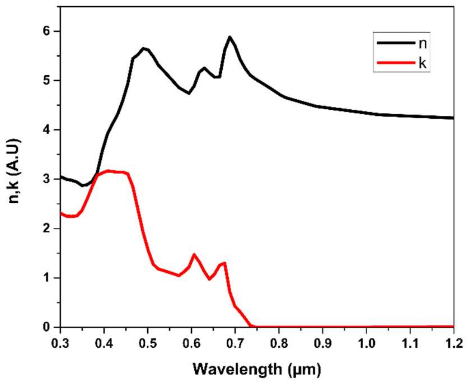
- Beal & Huges Refractive Index of MoS2 (Molybdenum Disulfide). Available online: https://refractiveindex.info/?shelf=main&book=MoS2&page=Beal (accessed on 1 April 2021).
- Yablonovitch, E.; Cody, G.D. Intensity Enhancement in Textured Optical Sheets for Solar Cells. IEEE Trans. Electron Devices 1982, 29, 300–305. [Google Scholar] [CrossRef]
- Beal, A.R.; Hughes, H.P. Kramers-Kronig analysis of the reflectivity spectra of 2H-MoS2, 2H-MoSe2 and 2H-MoTe2. J. Phys. C Solid State Phys. 1979, 12, 881. [Google Scholar] [CrossRef]
- Duan, W.; Bittkau, K.; Lambertz, A.; Qiu, K.; Yao, Z.; Steuter, P.; Qiu, D.; Rau, U.; Ding, K. Improved Infrared Light Management with Transparent Conductive Oxide/Amorphous Silicon Back Reflector in High-Efficiency Silicon Heterojunction Solar Cells. Sol. RRL 2021, 5, 2000576. [Google Scholar] [CrossRef]
- Hossain, M.I.; Qarony, W.; Hossain, M.K.; Debnath, M.K.; Uddin, M.J.; Tsang, Y.H. Effect of back reflectors on photon absorption in thin-film amorphous silicon solar cells. Appl. Nanosci. 2017, 7, 489–497. [Google Scholar] [CrossRef] [Green Version]
- SunSolve. Available online: https://www.pvlighthouse.com.au/sunsolve (accessed on 1 April 2021).
- Jung, G.H.; Yoo, S.J.; Park, Q.H. Measuring the optical permittivity of twodimensional materials without a priori knowledge of electronic transitions. Nanophotonics 2018, 8, 263–270. [Google Scholar] [CrossRef]
- Islam, K.M.; Synowicki, R.; Ismael, T.; Oguntoye, I.; Grinalds, N.; Escarra, M.D. In-Plane and Out-of-Plane Optical Properties of Monolayer, Few-Layer, and Thin-Film MoS2 from 190 to 1700 nm and Their Application in Photonic Device Design. Adv. Photonics Res. 2021, 2, 2000180. [Google Scholar] [CrossRef]
- McIntosh, K.R.; Jung, J.; Abbott, M.D.; Sudbury, B.A. Determination and evaluation of a backsheet’s intrinsic reflectance. AIP Conf. Proc. 2018, 1999, 020018. [Google Scholar] [CrossRef]
- Jäger, K.; Korte, L.; Rech, B.; Albrecht, S. Numerical optical optimization of monolithic planar perovskite-silicon tandem solar cells with regular and inverted device architectures. Opt. Express 2017, 25, A473. [Google Scholar] [CrossRef]
- Ganapati, V.; Steiner, M.A.; Yablonovitch, E. The Voltage Boost Enabled by Luminescence Extraction in Solar Cells. IEEE J. Photovolt. 2016, 6, 801–809. [Google Scholar] [CrossRef]
- Torres, I.; Fernández, S.; Fernández-Vallejo, M.; Arnedo, I.; Gandía, J.J. Graphene-Based Electrodes for Silicon Heterojunction Solar Cell Technology. Materials 2021, 14, 4833. [Google Scholar] [CrossRef]
- Schulman, D.S.; Arnold, A.J.; Das, S. Contact engineering for 2D materials and devices. Chem. Soc. Rev. 2018, 47, 3037–3058. [Google Scholar] [CrossRef]


| Device | Metal Contact Parameters |
|---|---|
| SSP Front Electrode | Ag-Dupont PV19, resistivity: 2.6 × 10⁻⁶ Ω·cm. Grid (H: 15 µm × W: 45 µm). Finger pitch (0.15 cm). Finger spacing (~0.14 cm) |
| SSP Back Electrode | Al-Paste, resistivity: 5 × 10⁻⁵ Ω·cm. Full contact |
| SSP Front Texturing | Random upright pyramids (Angle: 52, H: 5 µm, W: 7.813 µm) |
| SHJ Front Electrodes | Custom Ag, resistivity 5.0 × 10⁻⁶ Ω·cm. Grid (H: 30 µm × W: 45 µm). Finger pitch (0.13 cm). Finger spacing (0.12 cm) |
| SHJ Back Electrodes | Custom Ag, resistivity 5.0 × 10⁻⁶ Ω·cm. Grid (H: 30 µm × W: 45 µm). Finger pitch (0.13 cm). Finger spacing (0.12 cm) or full contact electrode |
| SHJ Front and Back Texturing | Random upright pyramids (Angle: 52, H: 5 µm, W: 7.813 µm) |
| Device | Device Ref. |
|---|---|
| SHJ | D1 |
| SHJ (150 µm)/MoS2 (~1 nm)/ITO (70 nm) | D2 |
| SHJ (150 µm)/MoS2 (~1 nm)/ITO (30 nm) | D3 |
| SHJ (150 µm)/ITO (30 nm)/MoS2 (~1 nm) | D4 |
| Device | FF (%) | Voc (mV) | Jsc (mA/cm2) | Efficiency-η (%) |
|---|---|---|---|---|
| SSP (170 µm) | 74.80 | 630.32 | 38.81 | 18.30 |
| SSP/MoS2 (170 µm/(~1 nm)) | 74.72 | 630.29 | 38.82 | 18.15 |
| SSP/MoS2 (170 µm/(~50.5 nm)) | 74.71 | 630.30 | 38.84 | 18.29 |
| SSP/MoS2 (170 µm/(~100 nm)) | 74.72 | 630.29 | 38.82 | 18.28 |
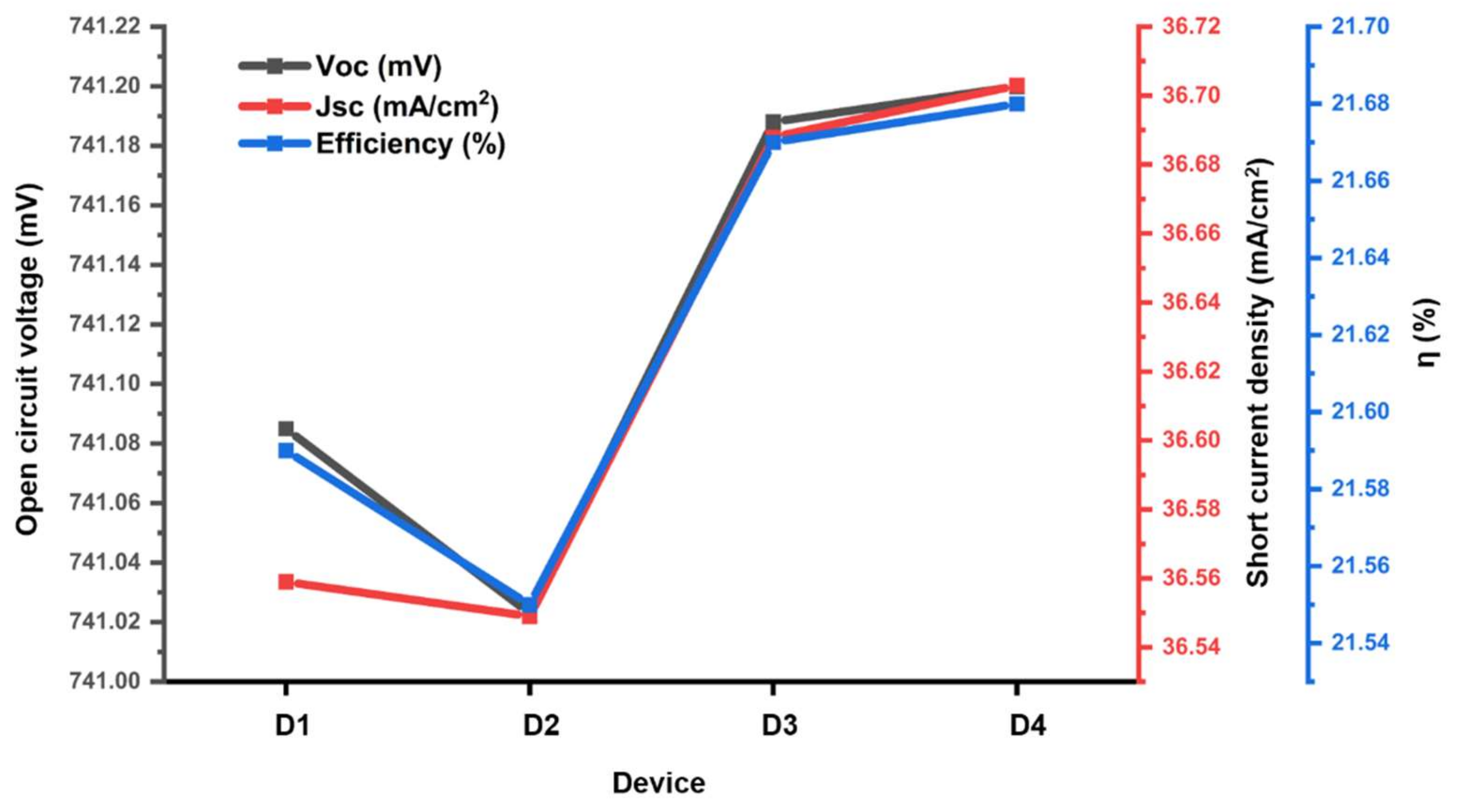
| Device | FF (%) | Voc (mV) | Jsc (mA/cm2) | Efficiency-η (%) |
|---|---|---|---|---|
| SHJ | 79.71 | 741.09 | 36.56 | 21.60 |
| SHJ/MoS2/ITO(170 µm/ (~1 nm)/70 nm) | 79.59 | 741.02 | 36.55 | 21.56 |
| SHJ/MoS2/ITO(170 µm/ (~1 nm nm)/30 nm) | 79.71 | 741.19 | 36.69 | 21.68 |
| SHJ/ITO/MoS2(170 µm/ (~30 nm)/1 nm) | 79.71 | 741.20 | 36.70 | 21.68 |
Publisher’s Note: MDPI stays neutral with regard to jurisdictional claims in published maps and institutional affiliations. |
© 2022 by the authors. Licensee MDPI, Basel, Switzerland. This article is an open access article distributed under the terms and conditions of the Creative Commons Attribution (CC BY) license (https://creativecommons.org/licenses/by/4.0/).
Share and Cite
Elsmani, M.I.; Fatima, N.; Torres, I.; Fernández, S.; Jallorina, M.P.A.; Chelvanathan, P.; Rais, A.R.M.; Daud, M.N.M.; Nasir, S.N.S.; Sepeai, S.; et al. Raytracing Modelling of Infrared Light Management Using Molybdenum Disulfide (MoS2) as a Back-Reflector Layer in a Silicon Heterojunction Solar Cell (SHJ). Materials 2022, 15, 5024. https://doi.org/10.3390/ma15145024
Elsmani MI, Fatima N, Torres I, Fernández S, Jallorina MPA, Chelvanathan P, Rais ARM, Daud MNM, Nasir SNS, Sepeai S, et al. Raytracing Modelling of Infrared Light Management Using Molybdenum Disulfide (MoS2) as a Back-Reflector Layer in a Silicon Heterojunction Solar Cell (SHJ). Materials. 2022; 15(14):5024. https://doi.org/10.3390/ma15145024
Chicago/Turabian StyleElsmani, Mohammed Islam, Noshin Fatima, Ignacio Torres, Susana Fernández, Michael Paul A. Jallorina, Puvaneswaran Chelvanathan, Ahmad Rujhan Mohd Rais, Mohd Norizam Md Daud, Sharifah Nurain Syed Nasir, Suhaila Sepeai, and et al. 2022. "Raytracing Modelling of Infrared Light Management Using Molybdenum Disulfide (MoS2) as a Back-Reflector Layer in a Silicon Heterojunction Solar Cell (SHJ)" Materials 15, no. 14: 5024. https://doi.org/10.3390/ma15145024