Article

Enhanced NO2 Sensing Performance of Graphene with Thermally Induced Defects

1
Sensor System Research Center, Korea Institute of Science and Technology (KIST), Seoul 02792, Korea
2
School of Engineering Technology, Purdue University, West Lafayette, IN 47907, USA
*
Author to whom correspondence should be addressed.
Materials 2021, 14(9), 2347; https://doi.org/10.3390/ma14092347
Submission received: 11 April 2021 / Revised: 28 April 2021 / Accepted: 29 April 2021 / Published: 30 April 2021

Abstract

:
This paper demonstrates the enhanced NO2 sensing performance of graphene with defects generated by rapid thermal annealing (RTA). A high temperature of RTA (300–700 °C) was applied to graphene under an argon atmosphere to form defects on sp2 carbon lattices. The density of defects proportionally increased with increasing the RTA temperature. Raman scattering results confirmed significant changes in sp2 bonding. After 700 °C RTA, ID/IG, I2D/IG, and FWHM (full width at half maximum)(G) values, which are used to indirectly investigate carbon-carbon bonds’ chemical and physical properties, were markedly changed compared to the pristine graphene. Further evidence of the thermally-induced defects on graphene was found via electrical resistance measurements. The electrical resistance of the RTA-treated graphene linearly increased with increasing RTA temperature. Meanwhile, the NO2 response of graphene sensors increased from 0 to 500 °C and reached maximum (R = ~24%) at 500 °C. Then, the response rather decreased at 700 °C (R = ~14%). The results imply that rich defects formed at above a critical temperature (~500 °C) may damage electrical paths of sp2 chains and thus deteriorate NO2 response. Compared to the existing functionalization process, the RTA treatment is very facile and allows precise control of the NO2 sensing characteristics, contributing to manufacturing commercial low-cost, high-performance, integrated sensors.

1. Introduction

Since the first demonstration of two-dimensional (2D) graphene devices by Andre Geim and Konstantin Novoselov [1], graphene-related researches have increased explosively owing to the excellent electrical [2,3,4], thermal [5], mechanical [6], and chemical [7] properties of graphene. In particular, graphene is considered a very promising gas sensing material. As a representative 2D material, graphene has a high surface-to-volume ratio (~2600 m2/g), facilitating the adsorption of gas molecules [8,9]. Furthermore, its low thermal-noise property improves its detection limit [10], and ultra-high carrier mobility (200,000 cm2/Vs) [2] and thermal conductivity (5000 Wm−1 K1) [5] can guarantee rapid transport of electrical signal induced by gas adsorption.
Based on the material properties as mentioned above, various graphene sensors for the detection of O2 [11], CO2 [12], NH3 [13,14], H2S [15], et cetera [8] have been studied, demonstrating competitive gas sensing performance compared to existing metal oxide gas sensors. In most studies till now, enhanced gas responsivity and selectivity were associated with covalent functionalization [7], electrical field effect [10,13], and heterojunction with nanomaterials [8,15]. However, these enhancement techniques are not practical due to unstable adsorption of functional or decoration materials on graphene and complex fabrication of sensor structures (e.g., three-terminal electrodes).
Recently, facile methods based on the formation of lattice defects (mostly vacancies) on graphene sensing channels were studied to improve the sensing performance [9,16]. Lee et al. reported that lattice defects could be readily formed on graphene physically via reactive ion etching (RIE), and their sensors showed remarkable responsivity enhancement in NO2 and NH3 detection. Furthermore, they demonstrated that the defect sites could be energetically more favorable for functionalization or decoration with nanomaterials. Although the RIE technique is very facile and appropriate for mass production, the accumulated damage to carbon-carbon bonds and increased oxidation sites after ion bombardment process severely affected charge transport property, and as such, the responsivity was decreased.
This report successfully demonstrates a facile method of creating graphene defects via rapid thermal annealing (RTA) to improve the performance of NO2 gas sensors. The generated graphene defects were confirmed by Raman spectra before and after RTA treatment. The RTA-treated graphene showed a remarkable increase in electrical resistance at metal-graphene-metal (MGM) contacts. Meanwhile, the NO2 response of graphene sensors exhibited the maximum responsivity of 24% and the response time of 111 s after the RTA treatment at 500 °C, which is about a two-fold enhancement compared with pristine (not RTA treated) graphene sensor (14%/304 s). Our results suggest that the RTA treatment can be a breakthrough approach to improving the NO2 sensing characteristics at low cost, thus contributing to manufacturing commercial low-cost, high-performance, integrated sensors.

2. Materials and Methods

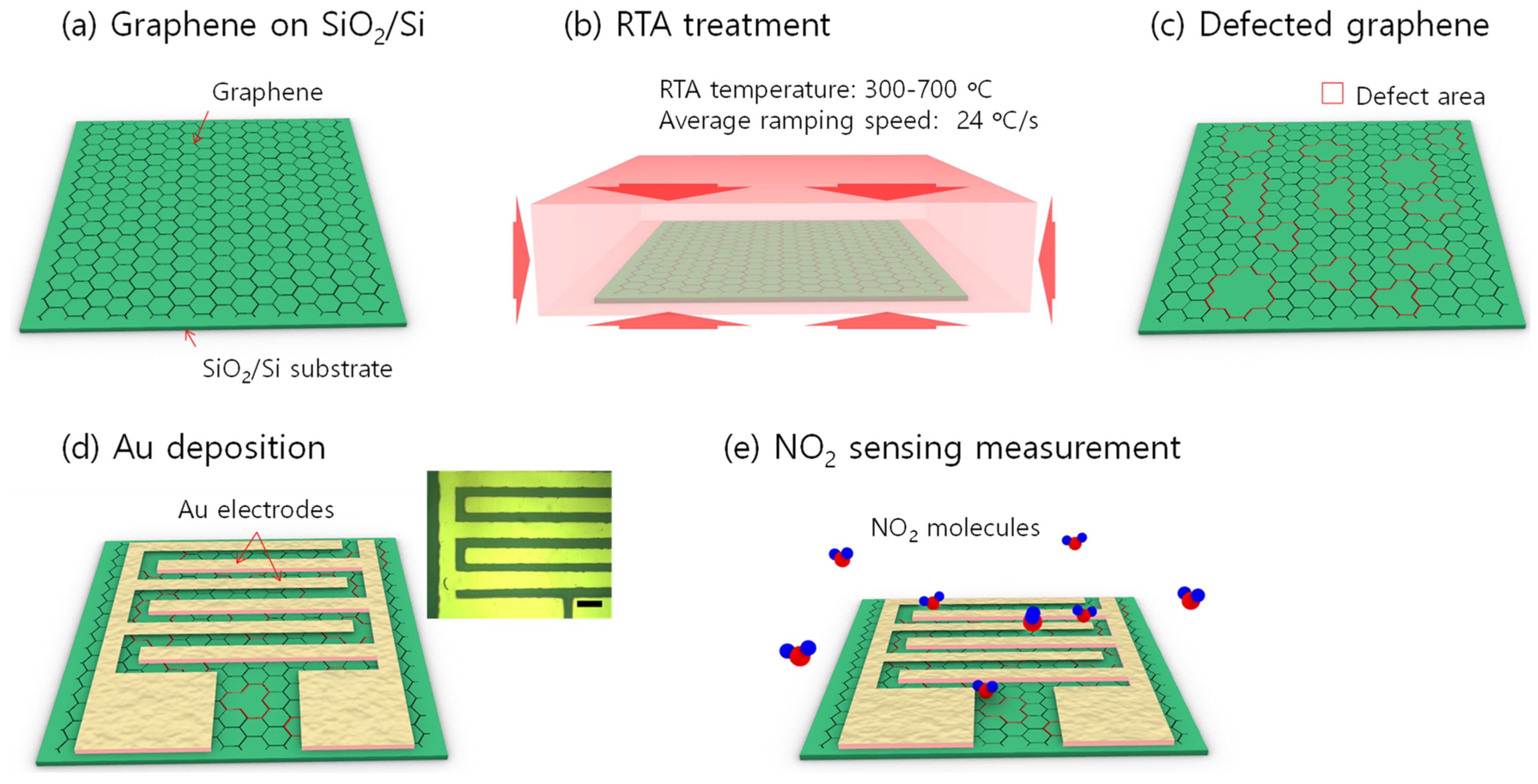
2.1. Generation of Graphene Defects by RTA Process

The purchased graphene on SiO2/Si substrate (Graphene Square Inc., Suwon, Korea) was used without further treatment, and the customized RTA system (see supplementary Figure S1) was utilized to generate graphene defects. The graphene sample was placed in the RTA chamber under an argon atmosphere. Then, the temperature of the chamber was rapidly increased to a target value in 20 s. Three RTA temperatures (300, 500, and 700 °C) were applied. After maintaining the heating state for an hour, the chamber naturally cooled down to room temperature.

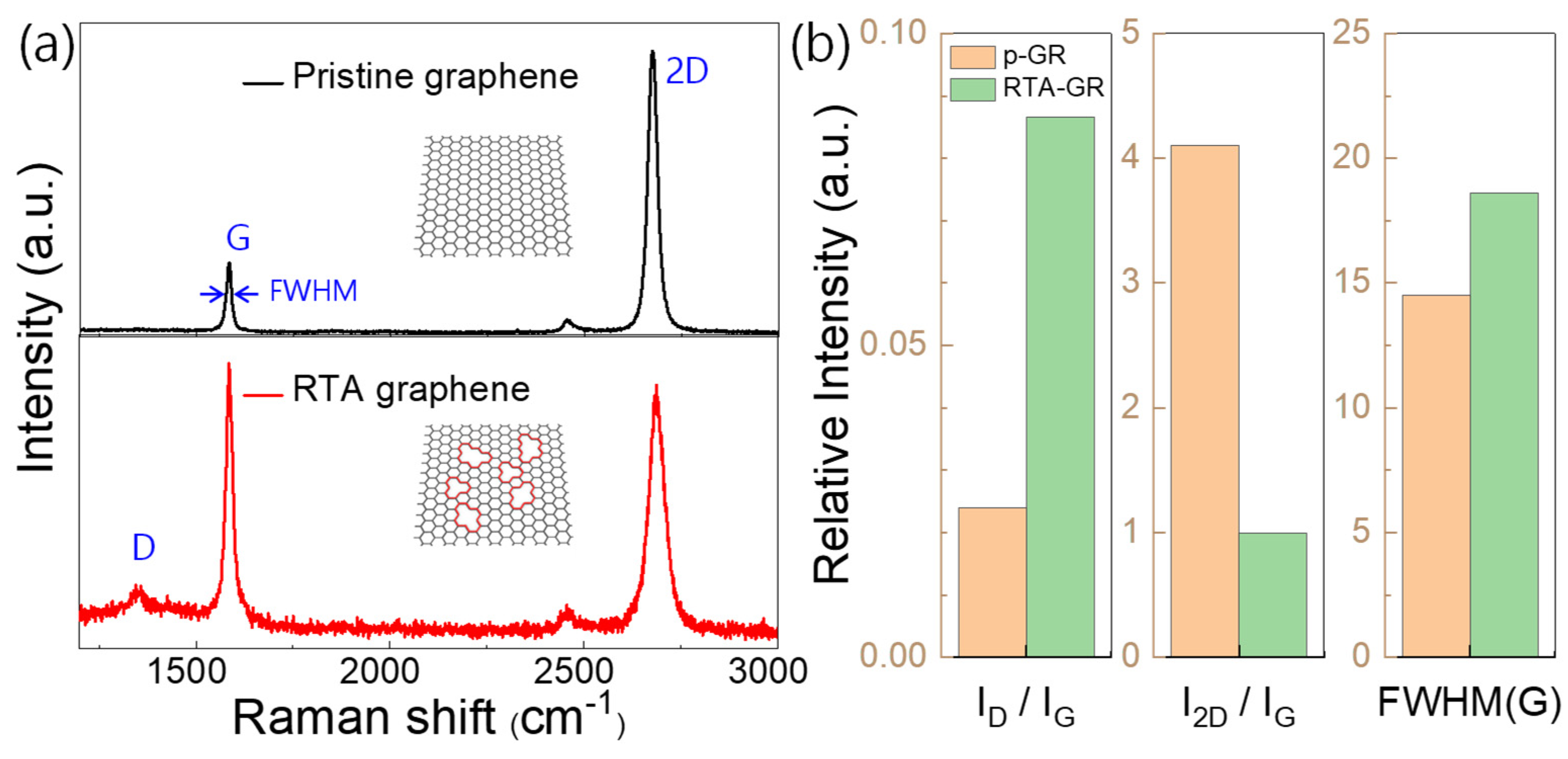
2.2. Raman Spectra Analysis

Raman spectra were recorded using an InVia Raman microscope (Renishaw Ltd., Gloucestershire, UK) and Nd:YAG laser (λ = 532 nm) at room temperature. The laser power was kept below 1 mW and the grating was 2400 L/mm. Wire program (version 3.4) was utilized to precisely designate peak position and intensity.

2.3. Fabrication of Graphene Gas Sensors

A shadow mask was used in DC magnetron sputtering process (SC-701MK II Advance, Sanyu Electron Co., Tokyo, Japan) to construct interdigitated gold (Au) electrodes. During the sputtering, ~315 VDC was applied under an argon atmosphere (Pressure: ~7.0 Pa). The sputtering continued for 7 min with a deposition rate of ~0.5 nm/s. The spacing and the thickness of the electrodes were 100 μm and 200 nm, respectively.

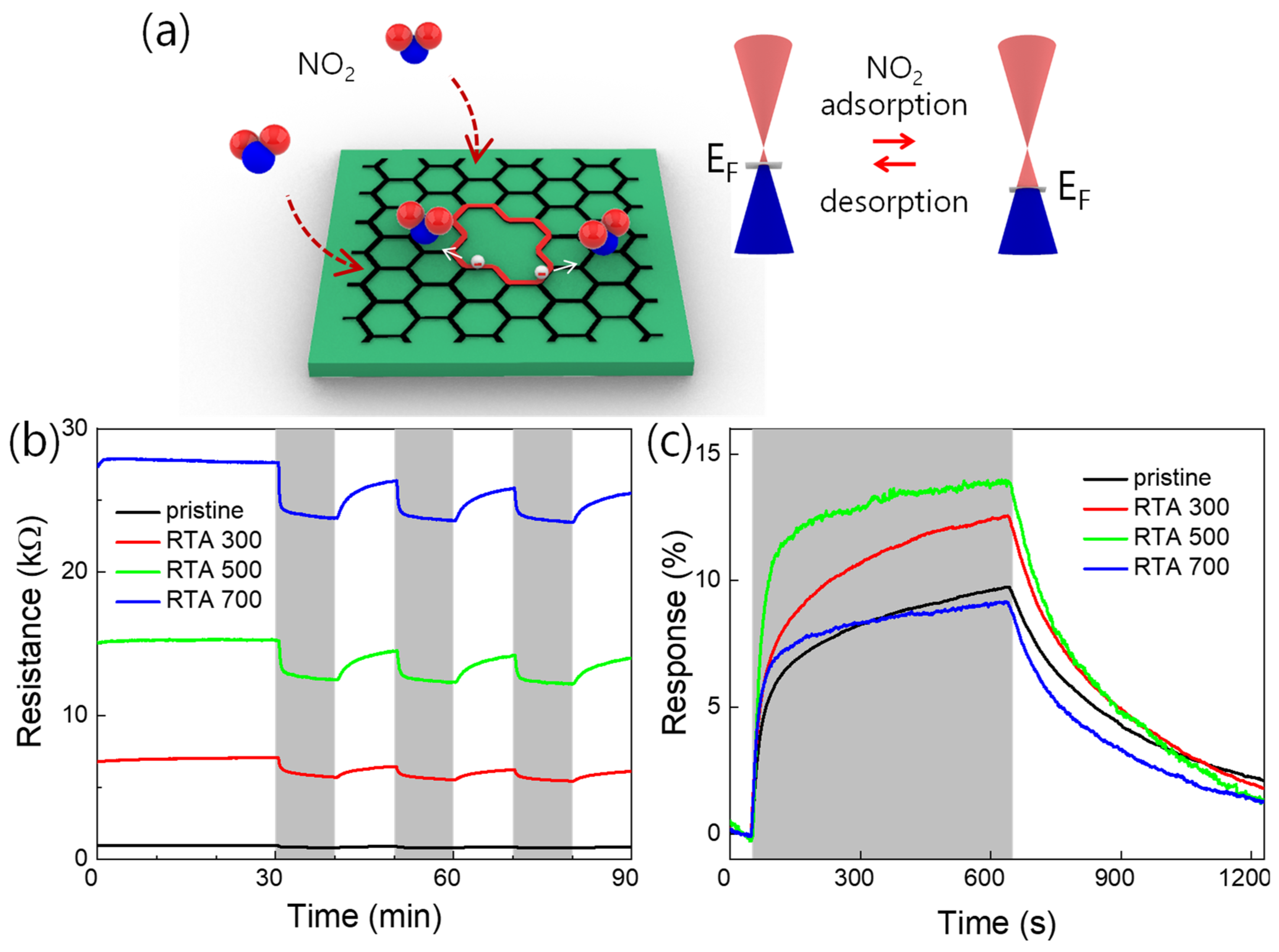
2.4. Nitrogen Dioxide (NO2) Sensing Measurements

The NO2 responsivity of the graphene sensor was analyzed in the custom-built measurement system (the temperature of the sample stage was maintained at 150 °C to improve the sensor’s recovery performance). At first, dry air as a balance gas was injected at 1 VDC and maintained for 20 min to eliminate unwanted gases and water molecules in the chamber. Then, the NO2 valve was opened, and the total flow, including the balance and target gases, was 500 sccm. The change in electrical resistance in response to the NO2 adsorption was recorded through electrical feed-throughs connecting to a SourceMeter (Model 2400, Keithley Instrument Inc., Cleveland, OH, USA) and sent to Lab-view software via a GPIB-to-USB converter for data collection and analysis.

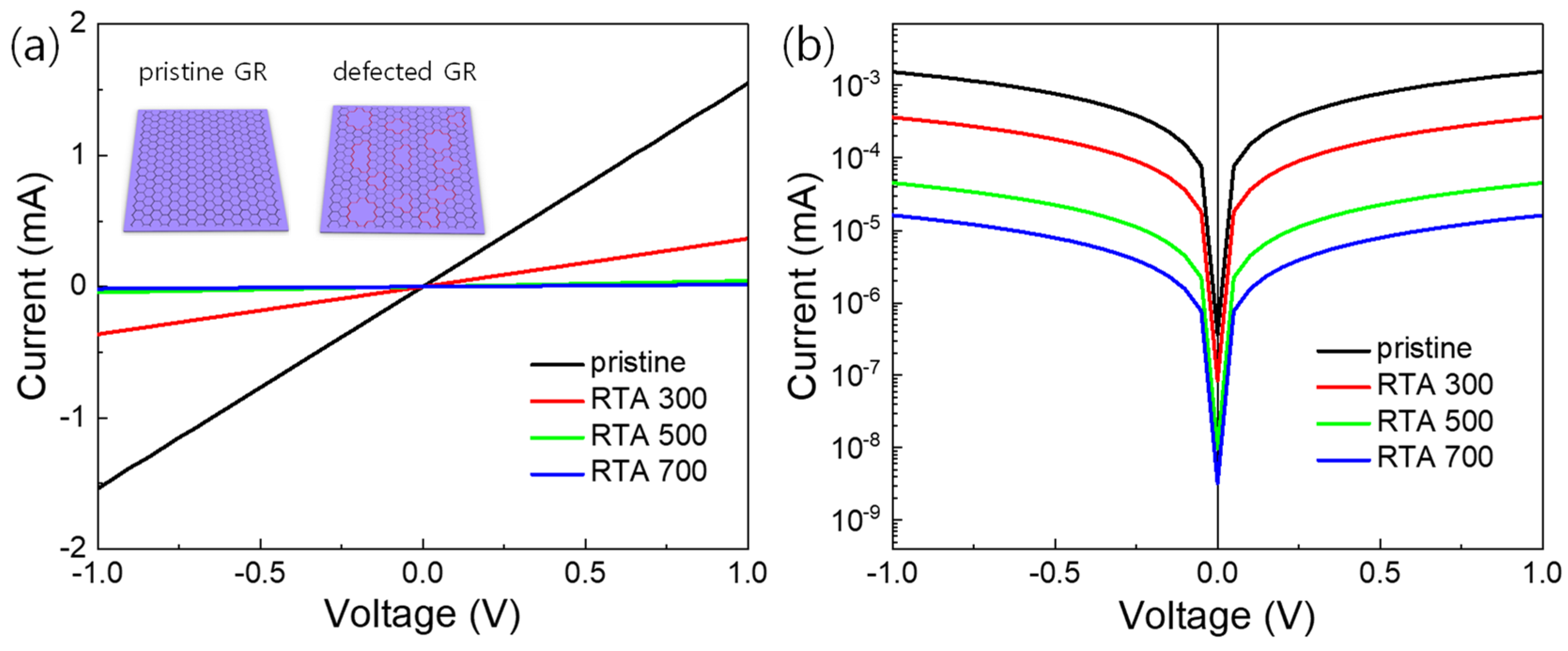
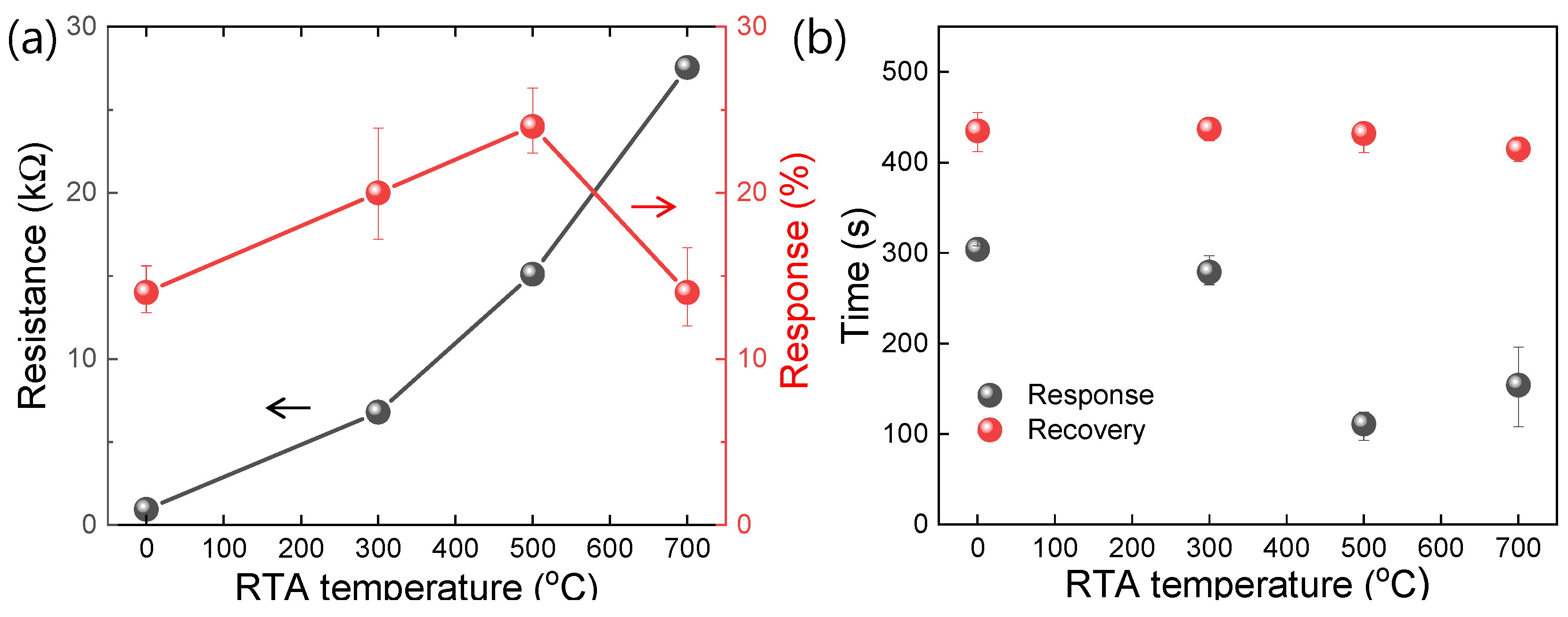
3. Results and Discussion

A schematic fabrication process of the defected graphene-based gas sensor is shown in Figure 1. The purchased graphene on SiO2/Si substrate was used without further treatment (a), and the rapid thermal annealing (RTA) process was utilized to generate defects in graphene lattices (b). Previously, the RTA process was reported as a tool for generating defects on single-walled carbon nanotube (SWCNT) walls [17,18,19]. Therefore, we expected the same effect of RTA (i.e., generating defects) on graphene whose lattice structure is the same as the SWCNTs. The graphene defects were generated by increasing the RTA temperature rapidly to the target value under an inert argon atmosphere. We tested three different RTA temperatures, namely, 300, 500, and 700 °C. Here, the average ramping speed was ~24 °C/s. The RTA-generated graphene defects were confirmed by Raman spectra in comparison with those of pristine graphene (c) (the details are discussed in Figure 2). We also confirmed the graphene defects indirectly by a transmission electron microscope (TEM) image of SWCNT defects generated at the same RTA condition (see Figure S2).
Subsequently, Au-electrodes were sputtered through a shadow mask to fabricate the metal-graphene-metal (MGM) structured device (d). Au is generally used as electrode material in graphene devices because of its low contact resistance with graphene [20]. The inset shows an optical image of the fabricated device. Finally, the NO2 sensing performance of the fabricated device was measured in a custom-built measurement system (e). The used measurement system is further discussed in Figure S3.
Figure 2a shows the Raman spectra of pristine graphene and 700 °C RTA-treated graphene, respectively (insets show schematic sample images). In both cases, graphene lattices were identified by two characteristic peaks (G peaks and 2D peaks at 1590 cm−1 and 2700 cm−1, respectively). Particularly in the case of pristine graphene (upper), D peak (at 1350 cm−1) is very weak and the I2D/IG value is relatively high as ~4, demonstrating a defect-free graphene monolayer [21] (here, I2D and IG refer to the intensities of 2D peaks and G peaks, respectively). On the other hand, the RTA-treated graphene shows an increased D peak intensity with a decreased I2D/IG value as ~1 in its Raman spectrum (lower), demonstrating the RTA-generated defects. Furthermore, three typical parameters extracted from each Raman spectrum are compared regarding the graphene qualities in Figure 2b. The ID/IG value increased from 0.024 to 0.065, meaning increased defect density after RTA treatment. Furthermore, the I2D/IG value decreased from 4.1 to 1.0, and the FWHM(G) value increased from 14.5 to 18.6 (here, FWHM refers to the full width at half maximum). These parameters are generally utilized for evaluating the graphene quality, and all the parameter value changes demonstrated the degradation of graphene quality, implying the increased defect density of graphene [22,23,24].
Figure 3a shows a comparison of the current-voltage (I–V) curves of the MGM devices fabricated with pristine graphene and RTA-treated graphene samples at 300, 500, and 700 °C (insets show the schematic sample images). As the RTA temperature increases, the current level of the corresponding device gradually decreases. The result suggests that defects are generated in graphene lattices by a high-temperature RTA treatment, and the defect density increases with increasing the RTA temperature. The variation of current levels depending on RTA temperature is similar to those in previous studies using SWCNTs (a carbon allotrope with the same sp2 lattices) [17,18,19], suggesting that defect-formation by RTA treatment is also applicable to graphene. Figure 3b shows the I–V curves on a logarithmic scale. The curves are symmetrical with respect to the line ‘V = 0’. The I–V curves’ linearity and symmetry demonstrate the ohmic contact between graphene and the sputtered Au electrodes [25].
Additionally, NO2 gas sensing performance of the fabricated device was studied. The expected NO2 sensing mechanism of the defected graphene device is described in Figure 4a. In general, graphene behaves as p-type material in the air by the following reaction [20,21].
O 2 + 2 H 2 O + 4 e 4 OH
when NO2 molecules adsorb onto the graphene surface, the concentration of major carriers (i.e., holes) increases by the following reaction [26].
NO 2 NO 2 + h +
Meanwhile, the RTA-generated defect regions (highlighted by a red line) are locally electron-abundant due to the presence of oxygen-containing functional groups (e.g., epoxy-, carbonyl-, and ether groups) [16]. Thus, adsorption of the electron-withdrawing NO2 molecules is promoted, which enhances the NO2 response. The resistance change can be explained by the Fermi level shift (see the inset of Figure 4a). Here, the oxygen-containing functional groups are expected to generate when the defected graphene is exposed to air.
Figure 4b shows a comparison of time-dependent resistance curves measured with four different graphene-based NO2 sensors (pristine graphene and RTA-treated graphenes at 300, 500, and 700 °C, respectively). The gray areas indicate where the target gas is injected. Here, the target- and base gases are 5 ppm NO2 (balanced by N2) and dry air, respectively, and 1 VDC was applied for each measurement. Additionally, the temperature of the sample stage was maintained at 150 °C during the measurement to improve the recovery performance. As the RTA temperature increased, the resistance of the corresponding device also increased. This is because the defect density increases as the temperature increases, as discussed above. However, in all the cases, the resistance decreased when the device was exposed to NO2 gas, meaning that all the device channels are p-type without polarity change.
The time-dependent response curves are compared in Figure 4c. The response is defined by the following formula.
R e s p o n s e   ( R ,   % ) = ( R g R 0 ) × 100 R 0
Here, Rg and R0 are the minima- and maxima resistance values, respectively, in the area where target gas is injected. As the RTA temperature increases from 0 to 500 °C, the response of the corresponding device increases. However, the response somewhat decreases in the case of the RTA-treated sample at 700 °C. This phenomenon can be understood as the defect density increased as the RTA temperature increased, and the lattice structures were significantly damaged by high thermal energy at above a critical RTA temperature, resulting in deterioration of NO2 response.
In Figure 5a, the resistance and response values are quantitatively compared depending on RTA temperature. Note that the resistance and response refer to each response curve’s initial resistance value and the average of three response values, respectively, in Figure 4b. As the RTA temperature increased, the resistance of the corresponding graphene device also increased. Interestingly, when the RTA temperature increased to 500 °C, the response increased to ~24%. However, the response decreased to ~14% in the case of RTA treatment at 700 °C. As discussed above, this result can be understood as the defect density increasing as the RTA temperature increases. However, the lattice structure partially collapsed, and the gas response decreased above a critical RTA temperature. The result suggests that if a defected graphene prepared under the optimal RTA condition is used for a sensing material, the off current (Ioff) can be reduced, and the response can be enhanced as well.
Additionally, each reaction curve’s response- and recovery times are compared (Figure 5b). The response (or recovery) time is defined as the elapsed time to reach 90% (or 10%) of the maximum response value from the turn-on (or turn-off) time. Interestingly, the response time tends to decrease as the RTA temperature increases (304 s for the 0 °C RTA sample and 154 s for the 700 °C RTA sample). The calculation process is discussed more in Figure S4. This phenomenon can be understood as a fact that the adsorption of electron-withdrawing NO2 gas molecules is promoted by the electron-abundant defected area as discussed above. However, the recovery times are almost the same for all the samples (~430 s), meaning that the RTA-generated defects do not affect the desorption rate of NO2 molecules.

4. Conclusions

In this paper, we demonstrated that graphene defects could be generated by RTA processes, and they could be utilized in high-performance NO2 sensors. As the RTA temperature increased from 300 to 700 °C, the corresponding device’s resistance gradually increased, whereas the NO2 response increased to 500 °C and decreased at 700 °C. This is because the defect density increased as the RTA temperature increased, and the graphene lattice is highly damaged above a critical RTA temperature, resulting in the deterioration of NO2 response. Interestingly, as the RTA temperature increased, the corresponding sensor’s response time decreased. The result implies that adsorption of NO2 molecules is promoted by the electron-abundant graphene defect areas. Our results suggest that the RTA process can be utilized to generate tunable graphene defects, and the defected graphene can be applied to high-performance gas sensor studies.

Supplementary Materials

The following are available online at https://www.mdpi.com/article/10.3390/ma14092347/s1, Figure S1: The customized RTA system; photographs of (a) front and (b) back sides of the equipment, (c) a picture inside the RTA chamber (inset shows a schematic structure). Figure S2: TEM image of the RTA-generated defected SWCNTs. Figure S3: The customized gas sensing measurement system; (a) a photograph of the system, (b) a schematic image of the system, pictures (c) inside the gas chamber and (d) of the gas chamber during measurement. Figure S4: Comparison of response times of the defected graphene-based NO2 sensors (each figure shows the typical response curve of the NO2 sensor prepared with RTA-treated graphene); (a) pristine graphene, (b) 300 °C -, (c) 500 °C -, and (d) 700 °C RTA graphenes.

Author Contributions

Conceptualization, N.L. and Y.P.; methodology, N.L. and H.K.; data curation, N.L. and Y.P.; project administration, Y.T.B.; supervision, Y.T.B.; writing—original draft, N.L.; writing—review and editing, Y.P. and Y.T.B. All authors have read and agreed to the published version of the manuscript.

Funding

This research was supported by the National Research Council of Science and Technology (NST) funded by the Korea government (MISP) (No. QLT-CRC-18-02-KICT) and a National Research Foundation of Korea (NRF) grant funded by the Korea government (MSIT, MOE) (No. 2019M3E7A1113097).

Institutional Review Board Statement

Not applicable.

Informed Consent Statement

Not applicable.

Data Availability Statement

All data has been included in the paper.

Conflicts of Interest

The authors declare no conflict of interest.

References

  1. Novoselov, K.S.; Geim, A.K.; Morozov, S.V.; Jiang, D.; Zhang, Y.; Dubonos, S.V.; Grigorieva, I.V.; Firsov, A.A. Electric Field Effect in Atomically Thin Carbon Films. Science 2004, 306, 666–669. [Google Scholar] [CrossRef] [PubMed] [Green Version]
  2. Bolotin, K.I.; Sikes, K.J.; Jiang, Z.; Klima, M.; Fudenberg, G.; Hone, J.; Kim, P.; Stormer, H.L. Ultrahigh electron mobility in suspended graphene. Solid State Commun. 2008, 146, 351–355. [Google Scholar] [CrossRef] [Green Version]
  3. Geim, A.K.; Novoselov, K.S. The rise of graphene. Nat. Mater. 2007, 6, 183–191. [Google Scholar] [CrossRef] [PubMed]
  4. Geim, A.K. Graphene: Status and Prospects. Science 2009, 324, 1530–1534. [Google Scholar] [CrossRef] [PubMed] [Green Version]
  5. Jauregui, L.A.; Yue, Y.; Sidorov, A.N.; Hu, J.; Yu, Q.; Lopez, G.; Jalilian, R.; Benjamin, D.K.; Delk, D.A.; Wu, W.; et al. Thermal Transport in Graphene Nanostructures: Experiments and Stimulations. ECS Trans. 2010, 28, 73–83. [Google Scholar] [CrossRef] [Green Version]
  6. Lee, C.; Wei, X.; Kysar, J.W.; Hone, J. Measurement of the Elastic Properties and Intrinsic Strength of Monolayer Graphene. Science 2008, 321, 385–388. [Google Scholar] [CrossRef]
  7. Kuila, T.; Bose, S.; Mishra, A.K.; Khanra, P.; Kim, N.H.; Lee, J.H. Chemical functionalization of graphene and its applications. Prog. Mater. Sci. 2012, 57, 1061–1105. [Google Scholar] [CrossRef]
  8. Sun, D.; Luo, Y.; Debliquy, M.; Zhang, C. Graphene-enhanced metal oxide gas sensors at room temperature: A review. Beilstein J. Nanotechnol. 2018, 9, 2832–2844. [Google Scholar] [CrossRef]
  9. Ma, J.; Zhang, M.; Dong, L.; Sun, Y.; Su, Y.; Xue, Z.; Di, Z. Gas sensor based on defective graphene/pristine graphene hybrid towords high sensitivity detection of NO2. AIP Adv. 2019, 9, 075207. [Google Scholar] [CrossRef] [Green Version]
  10. Inaba, A.; Yoo, K.; Takei, Y.; Matsumoto, K.; Shimoyama, I. Ammonia gas sensing using a graphene field-Effect transistor gated by ionic liquid. Sens. Actuator B Chem. 2014, 195, 15–21. [Google Scholar] [CrossRef]
  11. Chen, C.W.; Hung, S.C.; Yang, M.D.; Yeh, C.W.; Wu, C.H.; Chi, G.C.; Ren, F.; Pearton, S.J. Oxygen sensors made by monolayer graphene under room temperature. Appl. Phys. Lett. 2011, 99, 243502. [Google Scholar] [CrossRef] [Green Version]
  12. Yoon, H.J.; Jun, D.H.; Yang, J.H.; Zhou, Z.; Yang, S.S.; Cheng, M.M.-C. Carbon dioxide gas sensor using a graphene sheet. Sens. Actuator B Chem. 2011, 157, 310–313. [Google Scholar] [CrossRef]
  13. Gautam, M.; Jayatissa, A.H. Graphene based field effect transistor for the detection of ammonia. J. Appl. Phys. 2012, 112, 064304. [Google Scholar] [CrossRef]
  14. Romero, H.E.; Joshi, P.; Gupta, A.K.; Gutierrez, H.R.; Cole, M.W.; Tadigadapa, S.A.; Eklund, P.C. Adsorption of ammonia on graphene. Nanotechnology 2009, 20, 245501. [Google Scholar] [CrossRef] [PubMed]
  15. Gutes, A.; Hsia, B.; Sussman, A.; Mickelson, W.; Zettl, A.; Carraro, C.; Maboudian, R. Graphene decoration with metal nanoparticles: Towards easy integration for sensing applications. Nanoscale 2012, 4, 438–440. [Google Scholar] [CrossRef] [PubMed]
  16. Lee, G.; Yang, G.; Cho, A.; Han, J.W.; Kim, J. Defect-engineered graphene chemical sensors with ultrajhigh sensitivity. Phys. Chem. Chem. Phys. 2016, 18, 14198–14204. [Google Scholar] [CrossRef] [PubMed]
  17. Kim, J.; Choi, S.-W.; Lee, J.-H.; Chung, Y.; Byun, Y.T. Gas sensing properties of defect-Induced single-Walled carbon nanotubes. Sens. Actuator B Chem. 2016, 228, 688–692. [Google Scholar] [CrossRef]
  18. Lim, N.; Kim, K.H.; Byun, Y.T. Preparation of defected SWCNTs decorated with en-APTAS for application in high-performance nitric oxide gas detection. Nanoscale 2021, 13, 6538–6544. [Google Scholar] [CrossRef]
  19. Jeong, D.-W.; Kim, K.H.; Kim, B.S.; Byun, Y.T. Characteristics of highly sensitive and selective nitric oxide gas sensors using defect-functionalized single-Walled carbon nanotubes at room temperature. Appl. Surf. Sci. 2021, 550, 149250. [Google Scholar] [CrossRef]
  20. Lim, N.; Yoo, T.J.; Kim, J.T.; Pak, Y.; Kumaresan, Y.; Kim, H.; Kim, W.; Lee, B.H.; Jung, G.Y. Tunable graphene doping by modulating the nanopore geometry on a SiO2/Si substrate. RSC Adv. 2018, 8, 9031–9037. [Google Scholar] [CrossRef] [Green Version]
  21. Kang, C.G.; Lee, Y.G.; Lee, S.K.; Park, E.; Cho, C.; Lim, S.K.; Hwang, H.J.; Lee, B.H. Mechanism of the effects of low temperature Al2O3 passivation on graphene field effect transistors. Carbon 2013, 53, 182–187. [Google Scholar] [CrossRef]
  22. Cancado, L.G.; Jorio, A.; Ferreira, E.H.M.; Stavale, F.; Achete, C.A.; Capaz, R.B.; Moutinho, M.V.O.; Lombardo, A.; Kulmala, T.S.; Ferrari, A.C. Quantifying defects in graphene via raman spectroscopy at different excitation energies. Nano Lett. 2011, 11, 3190–3196. [Google Scholar] [CrossRef] [PubMed] [Green Version]
  23. Eckmann, A.; Felten, A.; Mishchenko, A.; Britnell, L.; Krupke, R.; Novoselov, K.S.; Casiraghi, C. Probing the nature of defects in graphene by raman spectroscopy. Nano Lett. 2012, 12, 3925–3930. [Google Scholar] [CrossRef] [PubMed] [Green Version]
  24. Eckmann, A.; Felten, A.; Verzhbitskiy, I.; Davey, R.; Casiraghi, C. Raman study on defective graphene: Effect of the excitation energy, type, and amount of defects. Phys. Rev. B 2013, 88, 035426. [Google Scholar] [CrossRef] [Green Version]
  25. Du, J.; Xing, J.; Ge, C.; Liu, H.; Liu, P.; Hao, H.; Dong, J.; Zheng, Z.; Gao, H. Highly sensitive and ultrafast deep UV photodetector based on a β–Ga2O3 nanowire network grown by CVD. J. Phys. D Appl. Phys. 2016, 49, 425105. [Google Scholar] [CrossRef]
  26. Lim, N.; Lee, J.-S.; Byun, Y.T. Negatively-doped single-walled carbon nanotubes decorated with carbon dots for highly selective NO2 detection. Nanomaterials 2020, 10, 2509. [Google Scholar] [CrossRef]
Figure 1. The schematic fabrication process of the chemiresistive-type gas sensor using defected graphene; (a) Preparation of a graphene-transferred SiO2/Si substrate. (b) Rapid thermal annealing (RTA) treatment to form defects in graphene lattice. (c) Schematic image of the defected graphene. (d) Au electrode deposition by sputtering process with a shadow mask (inset shows an optical microscope image of the device (scale bar: 200 μm)). (e) NO2 gas sensing measurement in a custom-built gas sensing system.
Materials 14 02347 g001
Figure 2. Comparison of Raman spectra of pristine- and RTA-treated graphenes; (a) Raman spectra of pristine- (upper) and RTA-treated (lower) graphenes (each inset shows schematic sample image). (b) Comparison of ID/IG, I2D/IG, and FWHM(G) values of pristine- and RTA-treated graphenes which are extracted from the Raman spectra.
Materials 14 02347 g002
Figure 3. Comparison of the four current-voltage (I–V) curves of graphene-based MGM devices in (a) linear- and (b) logarithmic scales (The devices were fabricated with pristine graphene and RTA-treated graphenes at 300, 500, and 700 °C, respectively).
Materials 14 02347 g003
Figure 4. (a) Schematic illustration of the expected NO2 gas-sensing mechanism of the defected graphene. Comparisons of the time-dependent (b) resistance- and (c) response curves of the four MGM devices (pristine graphene and RTA-treated graphenes at 300, 500, and 700 °C, respectively).
Materials 14 02347 g004
Figure 5. (a) Variation of resistance and response values depending on the RTA temperature. (b) Comparison of the response- and recovery times of the devices depending on the RTA temperature.
Materials 14 02347 g005
Publisher’s Note: MDPI stays neutral with regard to jurisdictional claims in published maps and institutional affiliations.

