Article

Ground State Properties of the Wide Band Gap Semiconductor Beryllium Sulfide (BeS)

by
Blaise A. Ayirizia
*,
Janee’ S. Brumfield
,
Yuriy Malozovsky
and
Diola Bagayoko
*
Department of Mathematics and Physics, Southern University and A&M College, Baton Rouge, LA 70813, USA
*
Authors to whom correspondence should be addressed.
Materials 2021, 14(20), 6128; https://doi.org/10.3390/ma14206128
Submission received: 26 August 2021 / Revised: 10 October 2021 / Accepted: 12 October 2021 / Published: 15 October 2021
(This article belongs to the Special Issue Wide-Bandgap Materials and Applications)

Abstract

:
We report the results from self-consistent calculations of electronic, transport, and bulk properties of beryllium sulfide (BeS) in the zinc-blende phase, and employed an ab-initio local density approximation (LDA) potential and the linear combination of atomic orbitals (LCAO). We obtained the ground state properties of zb-BeS with the Bagayoko, Zhao, and Williams (BZW) computational method, as enhanced by Ekuma and Franklin (BZW-EF). Our findings include the electronic energy bands, the total (DOS) and partial (pDOS) densities of states, electron and hole effective masses, the equilibrium lattice constant, and the bulk modulus. The calculated band structure clearly shows that zb-BeS has an indirect energy band gap of 5.436 eV, from Γ to a point between Γ and X, for an experimental lattice constant of 4.863 Å. This is in excellent agreement with the experiment, unlike the findings of more than 15 previous density functional theory (DFT) calculations that did not perform the generalized minimization of the energy functional, required by the second DFT theorem, which is inherent to the implementation of our BZW-EF method.

1. Introduction

Group II–IV compounds have been widely studied in light of the growing demand for potentially good semiconductors for various electrical and optical devices. BeS is an interesting material with high hardness; it belongs to the beryllium chalcogenides family and crystallizes in the zinc-blende structure under normal condition. It has potential applications in blue-green laser diodes and light-emitting diodes. The material can be grown on various substrates by molecular beam epitaxy [1,2]. The toxicity of zb-BeS has partly resulted in the dearth of experimental results on its many properties. Muoz et al. [3] used first-principles calculations to show that BeS undergoes a phase transition to the nickel arsenide (NiAs) structure under high pressure. The band gaps of Be compounds are experimentally reported to range between 2.7 eV and 5.5 eV [4]. Ab-initio pseudopotential calculations [5] with the local density approximation (LDA) and the generalized gradient approximation (GGA) obtained an indirect band gap of 2.911 eV and 3.041 eV, respectively. The work of Gonzalez-Diaz et al. [6] employed the first-principles pseudopotential plane wave method and the Cerperly Alder form of the local density approximation potential, where they found an indirect band gap of 2.75 eV for zb-BeS. Benosman et al. [7] used the FP- LAPW method and a local density approximation for exchange and correlation potential to study the structural and electronic properties of BeS. They reported a band gap of 2.847 eV. Table 1 shows the findings from over 20 previous DFT calculations using ab-initio LDA or generalized gradient approximation (GGA) potentials. The 11 LDA calculations reported gaps in the 2.38 eV to 4.17 eV range. The nine (9) GGA computations found band gaps in the 3.041 eV to 4.241 eV range. These calculations not only disagree among themselves, but also with an experiment that produced a gap of 5.5 eV. The previous DFT calculations uniformly underestimated the band gap. Our motivation for this work stems from these disagreements and potential applications of zb-BeS. The results obtained with ad-hoc DFT potentials vary with the adjustable parameters germane to the construction of these potentials; consequently, we do not discuss here the calculations with these potentials due to their lack of predictive capabilities. Even though the Green function and dressed Coulomb approximation (GW) is beyond density functional theory, results from this approach, as per the content of the table, are also underestimates of the measured band gap of zb-BeS.
Engel and Vosko generalized-gradient approximation (EV-GGA) and screened exchange local density approximation (Sx-LDA).
This motivation is underscored by the fact that an accurate value of the band gap is necessary for producing correct, theoretical descriptions of electronic, optical, dielectric, transport, and related properties of semiconductors and insulators. Our computational method, described below, performs a generalized minimization of the energy functional to reach, verifiably, the ground state without using over-complete basis sets. In doing so, its results possess the full, physical content of DFT and generally agrees with the corresponding, experimental ones.

2. Computational Method and Related Details

We employed the Ceperley and Alder’s [20] local density approximation potential, which was parameterized by Vosko et al. [21]. Based on DFT, it fully minimized the energy functional with the Bagayoko, Zhao, and Williams (BZW) method [22,23,24], as enhanced by Ekuma and Franklin (BZW-EF) [25,26,27,28], while implementing the linear combination of atomic orbitals (LCAO). We employed a program package developed at the Ames Laboratory of the U.S. Department of Energy, Ames, Iowa [29,30].
We begin our self-consistent calculations with a small basis set that can account for all the electrons in the system under study. Calculation II uses the basis set of calculation I plus one orbital representing an excited state. The occupied energies of calculation I and calculation II were compared, graphically and numerically, with the Fermi energy set to zero. Some occupied energies from calculation II were lower than their values from calculation I. This lowering of occupied energies indicates that the basis set of calculation I is not complete for the description of the ground state. If it were, no augmented basis set would have lowered the occupied energies that have reached their absolute minima (i.e., the ground state). We have no proof that calculation II reached the ground state, so we continued the process of augmenting the basis set and of performing successive, self-consistent calculations. When three (3) consecutive calculations produced the same occupied energies, within our computational uncertainty of 5 meV, this is the proof that these energies have reached their absolute minima (i.e., the ground state). These three (3) calculations constitute the rigorous criteria for ending the process.
The first of the above referenced three (3) consecutive calculations, with the smallest basis set, provides the true DFT description of the material. The occupied energies of these calculations are unaffected (i.e., they do not change), however, the unoccupied energies from these calculations are either lower than or equal to their corresponding values produced with the optimal basis set [25,27,31]. In the discussion section, we address this extra-lowering of some unoccupied energies while the occupied ones remain unchanged. The most important thing to emphasize here is that unoccupied energy values that are lower than their corresponding values obtained with the optimal basis no longer belong to the spectrum of the Hamiltonian, a unique functional of the electronic density [25]. Another way of proving this fact follows. The charge density and the potential did no change from the first of the three (3) calculations to the last. Hence, the Hamiltonian, a unique function of the density, does not change either. Therefore, any unoccupied eigenvalues from the second or third of the three (3) calculations that is lowered than it corresponding value from the first calculation is not due to a physical interaction. Bagayoko [25] explained this fact and ascribed the lowering of these unoccupied energies to a mathematical artifact stemming from the Rayleigh theorem for eigenvalues. The theorem asserts the lowering of some eigenvalues with the increase in the dimension of the Hamiltonian matrix [30].
The computational details that permit the replication of this work are as follows: BeS crystallizes in the cubic 216 (Fm- 4 ¯ m) space group where the positions of the atoms of Be and S are (0,0,0) and (1/4,1/4,1/4), respectively, with an experimental lattice constant of 4.86 Å [32]. We began by performing self-consistent ab-initio calculations for the ionic species Be2+ and S2−, and we employed a set of even-tempered Gaussian exponents to expand the radial components of the atomic wave functions in terms of Gaussian functions. The s and p orbitals for the ionic species (Be2+ and S2−) were described using 16 and 22 even tempered Gaussian functions, respectively. For Be2+, the maximum and minimum exponents utilized were 0.9 × 10⁵ and 0.24, respectively, whereas for S2−, they were 0.24 × 10⁶ and 0.135, respectively. After 60 iterations, for 81 k-points in the irreducible Broullouin zone, self-consistency was achieved when the difference in the potential between two consecutive iterations was less than or equal to 10−5.

3. Results

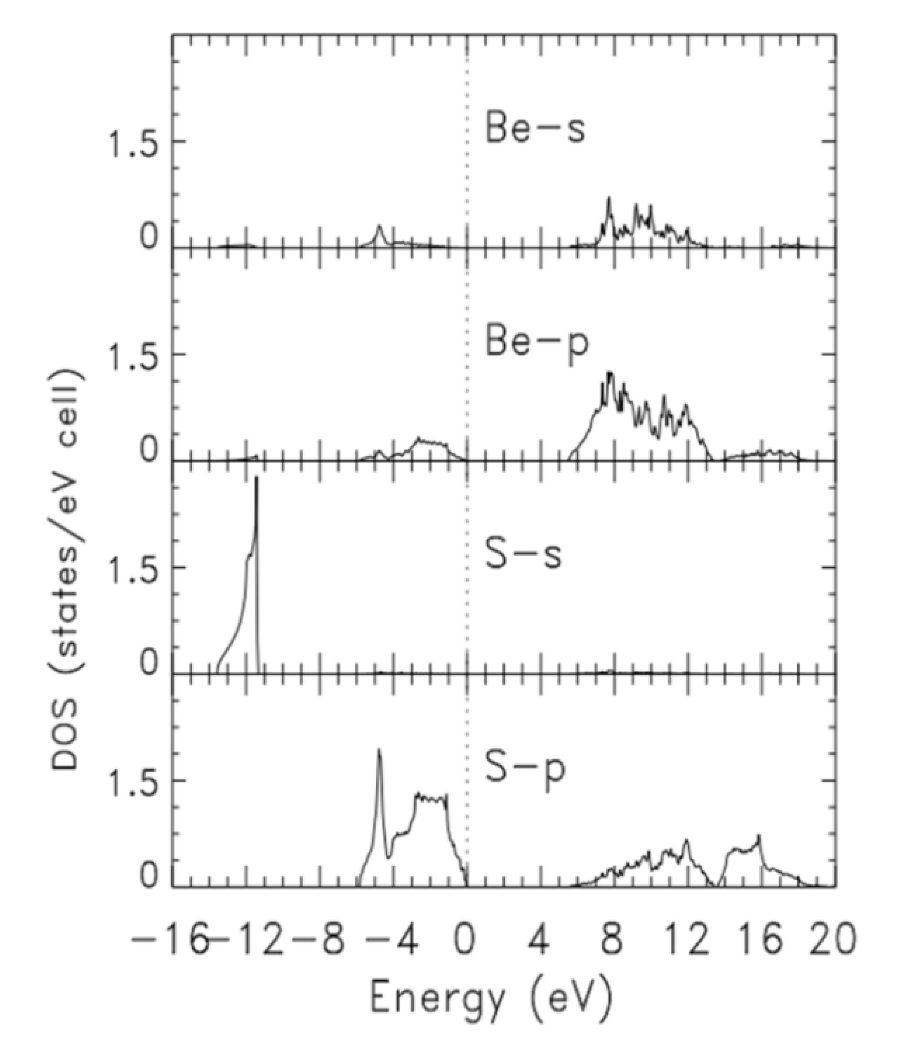
3.1. Electronic Properties

The valence orbitals in the basis set for the successive, self-consistent calculations with the BZW-EF computational method are listed in Table 2, along with the resulting band gaps. The occupied bands from calculations III–V are perfectly superimposed. Hence, they are the three (3) calculations producing the same, occupied energies that have reached their absolute minima (i.e., the ground state). Calculation III is therefore the one providing the true DFT description of zb-BeS. The calculated indirect band gap from Γ to a point between Γ and X was 5.436 eV. The minimum in the conduction band occurred along the Γ-X line, near the X point.
Figure 1 shows the electronic band structures of zb-BeS obtained from calculations III and IV. The bands from calculation III are in solid lines while those from calculation IV are in dashed lines. The occupied energies for both calculations (III and IV) are the same, as clearly shown by the perfect superposition of the valence bands from calculations III and IV. The fact that calculation V produced the same occupied energies signified that the ground state had been reached. Our work on GaP showed that the two consecutive calculations can produce the same occupied energies—as local minima—while the next calculation with an augmented basis sets further lowered some occupied energies. Among the three (3) calculations, the first had the smallest basis set called the optimal basis set.
Table 3 shows the electronic energies, obtained with the optimal basis set of calculation III, at high symmetry points in the Brillouin zone. The contents of this table lend themselves to comparison with results from future experimental findings such as the UV and X-ray spectroscopy experiments.
The calculated total density (DOS) and partial (pDOS) densities of states, are derived from the ground state band structure from calculation III. Figure 2 and Figure 3 show the DOS and pDOS, respectively, in the energy range of −16 eV to +20 eV. In both figures, the dashed, vertical line indicate the position of the Fermi level. While band widths and gaps can be estimated using Figure 2, their accurate values can be easily read from Table 2. The total valence band width and that of the lowest laying valence band were 13.585 eV and 2146 eV, respectively. The gap between the lowest laying band and the group of upper valence bands was 5.561 eV. We already noted the indirect band gap of 5.436 between the top of the valence band and the bottom of the conduction band. The width of the upper group of valence bands was 5.878 eV. As shown in Figure 3, the lowermost valence band is largely made up of S, with a faint contribution from Be s. The S p states contribute to the most to the upper group of valence bands, with relative small and tiny contributions from Be p and Be s, respectively. While Be p dominated at the very bottom of the conduction bands, the contributions of S p and Be s increased with energy, up to 12 eV.

3.2. Transport Properties

The determination of numerous material transport properties requires the use of effective masses. Electrical conductivity and mobility are two such quantities. We calculated electron effective masses around the minimum of the conduction band, while the heavy and light hole effective masses were calculated around the top of the valence band at the Γ point. We considered the (1,0,0), (1,1,0), and (1,1,1) directions for the hole effective masses. Our calculated effective masses are presented in part (a) for the electron and part (b) for the hole effective masses. The calculation performed by D.J Skutel [10], using a nonrelativistic formalism and slater’s free electron-exchange approximation, found the heavy hole and light hole at Γ in the (1,0,0) directions as 0.7 m0 and 0.4 m0, respectively, where m0 is the free electron mass. In (1,1,1), he found the effective masses for the heavy and light hole to be 1.7 m0 and 0.3 m0, respectively. Skutel also calculated the electron effective mass at the conduction band minimum, the (1,0,0) direction, as 1.0. This value is close to a third larger than our finding of 0.743.
As in the case of the electron effective mass in the (1,0,0) directions, the calculated hole effective masses from Skutel (10) were larger than the corresponding ones in part (b) of Table 4.

3.3. Structural Properties

The equilibrium lattice constant was determined to correspond to the minimum in the curve of the total energy versus the lattice constant, as shown in Figure 4. This predicted lattice constant was 4.814 Å for zb-BeS. This value is in good agreement with the first principle calculation finding of Okoye [17]. Our theoretical bulk modulus was 107.7 GPa. We compare our results to other theoretical calculations and experiments in Table 5.

4. Discussion

In this paper, we investigated the electronic, transport, and structural properties of beryllium sulfide in the zinc-blende phase, using the BZW-EF computational method and a local density approximation potential. Our study yielded an indirect band gap of 5.436 eV, with the minimum of the conduction band wis located at a point between Γ and the X point. The band structure shows that the minimum of the conduction band was located not at the X-point (where Eg = 6.5 eV) but shifted toward the Γ-point by 35% (by 0.35). The comprehensive description of our method [23,25] revealed a key distinction between BZW-EF calculations and other DFT calculations. We performed a generalized minimization of the energy in our self-consistent calculation to reach the ground state of the material, unlike other DFT calculations that employed a single basis set. As explained by Bagayoko [23], a single basis leads to a stationary state upon the attainment of self-consistency. These is an infinite number of such self-consistent results called stationary solutions. One cannot take any one of them arbitrarily to correspond to the ground state of the material. In these one basis set calculations, that basis set is generally selected to be quite large, in order to ensure completeness.
As explained by Bagayoko [25], when such a large basis set contains the optimal one, it leads to the ground state energies and to some unoccupied energies that are spuriously low by virtue of the Rayleigh theorem [30]. Specifically, these spurious, unoccupied energies are smaller than the corresponding unoccupied energies produced with the optimal basis set. As noted at the end of the presentation of our method, the referenced spurious lowering of unoccupied energies, with basis sets that are over-complete for the description of the ground state, is a plausible explanation of the general underestimation of the band gap by single basis set calculations such as the ones in Table 1. We should reiterate that the second theorem of DFT requires the generalized minimization of the energy functional to reach the ground state. As successively augmented basis sets produce energy functional that are lower for larger basis sets up the optimal one, the BZW-EF performs a generalized minimization of the energy far beyond any minimization that may result from self-consistent iterations with a single basis set. The above points are the reason our computational results possess the full, physical content of DFT and agree with the corresponding experimental ones, as is the case of the band gap of zb-BeS, for which we had a measured value around 5.5 eV. The theoretical bulk modulus from our work, 107.7 GPa, was about the same as the experimental result of 105 GPa of Narayana et al. [32].

5. Conclusions

By employing the BZW-EF computational method and a local density approximation potential, we studied the electronic, structural, and transport properties of the semiconductor BeS, in the zinc-blende phase. Our results for the first principle self-consistent calculations of the material and conclusion are summarized below. Our results possess the full, physical content of DFT by virtue of our generalized minimization of the energy functional (a) to reach the ground state while (b) avoiding over-complete basis sets. The electronic structure calculations showed that zb-BeS has an indirect band gap of 5.436 eV that agrees well with the available experimental value around 5.5 eV. Over 15 previous ab-initio LDA and GGA calculations uniformly underestimated this band gap by more than 50% in some cases, as per the contents in Table 1. As was the case in several previous studies by our group, some of which are listed below as references, future experiments are expected to confirm our results for which we could not find corresponding experimental ones. This assertion is expected to hold not only for the equilibrium lattice constant (4.814 Å), but also for the effective masses and the widths and other features of the band structures and related densities of states.

Author Contributions

Conceptualization, B.A.A. and D.B.; methodology, D.B.; software, D.B.; validation, B.A.A., J.S.B. and D.B.; formal analysis, Y.M.; investigation, Y.M. and J.S.B.; writing—original draft preparation, B.A.A.; writing—review and editing, B.A.A. and D.B.; supervision, D.B.; funding acquisition, D.B. All authors have read and agreed to the published version of the manuscript.

Funding

National Science Foundation [NSF, Award Nos. EPS-1003897, NSF (2010–2015)-RH SUBR, and HRD-1002541], the U.S. Department of Energy, National Nuclear Security Administration (NNSA, Award No. DE-NA0002630), LaSPACE, and LONI-SUBR.

Informed Consent Statement

Not applicable.

Data Availability Statement

The data presented in this study are available on request from the corresponding author.

Conflicts of Interest

The authors declare no conflict of interest.

References

  1. Landwehr, G. Molecular-beam epitaxy of beryllium-chalcogenide-based thin films and quantum-well structures. J. Appl. Phys. 1998, 792, 1–6. [Google Scholar]
  2. Ivanov, S.V.; Toropov, A.A.; Sorokin, S.V.; Shubina, T.V.; Il’inskaya, N.D.; Lebedev, A.V.; Sedova, I.V.; Kop’ev, P.S.; Alferov, Z.I.; Lugauer, H.J.; et al. Molecular beam epitaxy of alternating-strain ZnSe-based multilayer heterostructures for blue-green lasers. Semiconductors 1998, 32, 1137–1140. [Google Scholar] [CrossRef]
  3. Muñoz, A.; Rodríguez-Hernández, P.; Mujica, A. Ground-state properties and high-pressure phase of beryllium chalcogenides BeSe, BeTe, and BeS. Phys. Rev. B Condens. Matter Mater. Phys. 1996, 54, 11861–11864. [Google Scholar] [CrossRef] [PubMed]
  4. Yim, W.; Dismukes, P.; Stofko, J.; Paff, J. Synthesis and some properties of BeTe, BeSe and BeS. J. Phys. Chem. Solids 1972, 33, 501–505. [Google Scholar] [CrossRef]
  5. Elias, B. Theoretical investigation of the structural, electronic, elastic, and optical properties of zinc- blende bes under high pressure. Theor. Investig. 2013, 2, 4193–4204. [Google Scholar]
  6. Gonzalez-Diaz, M.; Rodriguez-Hernandez, P.; Munoz, A. Elastic constants and electronic structure of beryllium chalcogenides BeS, BeSe, and BeTe from first-principles calculations. Phys. Rev. B 1996, 55, 14043. [Google Scholar] [CrossRef]
  7. Benosman, N.; Amrane, N.; Méçabih, S.; Aourag, H. Structural and electronic properties of bulk BeS. Phys. B Condens. Matter 2001, 304, 214–220. [Google Scholar] [CrossRef]
  8. Van Camp, P.E. Ground state properties and structural phase transformation of beryllium sulphide, solid state communication. J. Phys. Condens. Matter 1996, 98, 741–743. [Google Scholar]
  9. Van Vechten, J.A. Quantum dielectric theory of electronegativity in covalent systems. II. Ionization potentials and interband transition energies. Phys. Rev. 1969, 187, 1007–1020. [Google Scholar] [CrossRef]
  10. Skutel, D.J. Energy band structure of BeS, BeSe, and BeTe. Phys. Rev. 1970, 2, 1852. [Google Scholar]
  11. Al-Douri, Y.; Baaziz, H.; Charifi, Z.; Reshak, A.H. Density functional study of optical properties of beryllium chalcogenides compounds in nickel arsenide B8 structure. Phys. B Condens. Matter 2012, 407, 286–296. [Google Scholar] [CrossRef]
  12. Guo, L.; Hu, G.; Zhang, S.; Feng, W.; Zhang, Z. Structural, elastic, electronic and optical properties of beryllium chalcogenides BeX (X = S, Se, Te) with zinc-blende structure. J. Alloys Compd. 2013, 561, 16–22. [Google Scholar] [CrossRef]
  13. Heciri, D.; Beldi, L.; Drablia, S.; Meradji, H.; Derradji, N.E.; Belkhir, H.; Bouhafs, B. First-principles elastic constants and electronic structure of beryllium chalcogenides BeS, BeSe and BeTe. Comput. Mater. Sci. 2007, 38, 609–617. [Google Scholar] [CrossRef]
  14. Srivastava, G.P.; Tütüncü, H.M.; Günhan, N. First-principles studies of structural, electronic, and dynamical properties of Be chalcogenides. Phys. Rev. B Condens. Matter Mater. Phys. 2004, 70, 1–6. [Google Scholar] [CrossRef]
  15. Faraji, S.; Mokhtari, A. Ab initio study of the stability and electronic properties of wurtzite and zinc-blende BeS nanowires. Phys. Lett. Sect. A Gen. At. Solid State Phys. 2010, 374, 3348–3353. [Google Scholar] [CrossRef] [Green Version]
  16. Yadav, P.S.; Yadav, R.K.; Agrawal, S.; Agrawal, B.K. Ab initio study of electronic and optical properties of Be-chalcogenides in GW approximation. Phys. E Low-Dimens. Syst. Nanostructures 2007, 36, 79–85. [Google Scholar] [CrossRef]
  17. Okoye, C.M.I. Structural, electronic, and optical properties of beryllium monochalcogenides. Eur. Phys. J. B 2004, 39, 5–17. [Google Scholar] [CrossRef]
  18. Wang, K.L.; Gao, S.P. Phonon dispersions, band structures, and dielectric functions of BeO and BeS polymorphs. J. Phys. Chem. Solids 2018, 118, 242–247. [Google Scholar] [CrossRef]
  19. Sarkar, R.L.; Chatterjee, S. Electronic energy bands of BeS, BeSe and BeTe. J. Phys. C Solid State Phys. 1977, 10, 57–62. [Google Scholar] [CrossRef]
  20. Alder, B.J.; Ceperley, D. Ground State of the Electron Gas by a Stochastic Method. Phys. Rev. Lett. 1980, 45, 566–569. [Google Scholar]
  21. Vosko, S.; Wilk, L.; Nusair, M. Accurate spin-dependent electron liquid correlation energies for local spin density calculations: A critical analysis. Can. J. Phys. 1980, 58, 1200–1211. [Google Scholar] [CrossRef] [Green Version]
  22. Bagayoko, D.; Zhao, G.L.; Fan, J.D.; Wang, J.T. Ab initio calculations of the electronic structure and optical properties of ferroelectric tetragonal BaTiO3. J. Phys. Condens. Matter 1998, 10, 5645–5655. [Google Scholar] [CrossRef]
  23. Franklin, L.; Ekuma, C.; Zhao, G.; Bagayoko, D. Bagayoko Density functional theory description of electronic properties of wurtzite zinc oxide. J. Phys. Chem. Solids 2013, 74, 729–736. [Google Scholar] [CrossRef]
  24. Bagayoko, D.; Franklin, L.; Zhao, G.L. Predictions of electronic, structural, and elastic properties of cubic InN. J. Appl. Phys. 2004, 96, 4297–4301. [Google Scholar] [CrossRef]
  25. Bagayoko, D. Understanding density functional theory (DFT) and completing it in practice. AIP Adv. 2014, 4, 127104. [Google Scholar] [CrossRef] [Green Version]
  26. Ayirizia, B.A.; Malozovsky, Y.; Franklin, L.; Bhandari, U.; Bagayoko, D. Ab-Initio Self-Consistent Density Functional Theory Description of Rock-Salt Magnesium Selenide (MgSe). Mater. Sci. Appl. 2020, 11, 401–414. [Google Scholar]
  27. Bagayoko, D. Understanding the Relativistic Generalization of Density Functional Theory (DFT) and Completing It in Practice. J. Mod. Phys. 2016, 7, 911–919. [Google Scholar] [CrossRef] [Green Version]
  28. Bhandari, U.; Ayirizia, B.A.; Malozovsky, Y.; Franklin, L.; Bagayoko, D. First principle investigation of electronic, transport, and bulk properties of zinc-blende magnesium sulfide. Electronics 2020, 9, 1791. [Google Scholar] [CrossRef]
  29. Feibelman, P.J.; Appelbaum, J.A.; Hamann, D.R. Electronic structure of a Ti(0001) film. Phys. Rev. B 1979, 20, 1433–1443. [Google Scholar] [CrossRef]
  30. Harmon, B.N.; Weber, W.; Hamann, D.R. Total-energy calculations for Si with a first-principles linear-combination-of-atomic-orbitals method. Phys. Rev. B 1982, 25, 1109–1115. [Google Scholar] [CrossRef]
  31. Ekuma, C.E.; Bagayoko, D. Ab-initio electronic and structural properties of rutile titanium dioxide. Jpn. J. Appl. Phys. 2011, 50, 2–9. [Google Scholar] [CrossRef] [Green Version]
  32. Narayana, C.; Nesamony, V.; Ruoff, A. Phase transformation of BeS and equation-of-state studies to 96 GPa. Phys. Rev. B Condens. Matter Mater. Phys. 1997, 56, 14338–14343. [Google Scholar] [CrossRef] [Green Version]
Figure 1. The electronic band structures of zb-BeS for a room temperature experimental lattice constant of 4.863 Å as obtained from calculations III (solid lines) and IV (dashed lines). Zero on the vertical axis denotes the position of the Fermi energy.
Materials 14 06128 g001
Figure 2. The total density of states (DOS) of zb-BeS, derived from the ground state band structure from calculation III.
Materials 14 06128 g002
Figure 3. Calculated partial densities of states (pDOS) of zb-BeS derived from the ground state band structure from calculation III.
Materials 14 06128 g003
Figure 4. The total energy versus the lattice constant for zb-BeS.
Materials 14 06128 g004
Table 1. Previous calculated indirect band gap of zb-BeS using various computational techniques and potentials.
Computational TechniquePotentialBand Gap, Eg (eV)
Pseudopotential Plane Wave (PP-PW)LDA2.911 [5]
PP-PWLDA2.75 [6]
PP-PWLDA2.816 [8]
Empirical Pseudopotential MethodLDA2.38 [9]
Orthogonalized Plane WaveLDA4.17 [10]
Full Potential Linearized Augmented Plane Wave (FP-LAPW)LDA2.828 [11]
PP-PWLDA2.912 [12]
Augmented plane Waves plus Local orbitals (APW + lo)LDA2.78 [13]
PP-PWLDA2.83 [14]
FP-LAPWLSDA2.847 [7]
PP-PWGGA3.041 [5]
PP-PWGGA3.7 [15]
PP-PWGGA3.192 [12]
PP-PWGGA3.11 [16]
FP-LAPWGGA3.141 [11]
FP-LAPWGGA3.13 [17]
Plane Wave pseudopotential (PW-PP)GGA3.15 [18]
APW + loPerdew-Burke-Erzerhof (PBE-GGA)3.10 [13]
PP-PWSx-LDA4.071 [12]
FP-LAPWEV-GGA4.241 [11]
Augmented Plane WaveHartee-Fock(HF)6.10 [19]
PW-PPQuansiparticle Self-Consistent Green’s Function (QPscGW)5.27 [18]
PW-PPGreen’s Function (GoWo)4.62 [18]
PP-PWGoWo4.45 [16]
Experiment using optical absorption measurement on the BeS platelets >5.5 [4]
Table 2. The successive, self-consistent calculations for zinc-blende beryllium sulfide, using the BZW-EF computational approach. We performed our calculation utilizing the experimental lattice constant of 4.86 Å.
Calculation NumberBeryllium (Be2+)Sulfur (S2−)
(1s22s22p6 in Core)
No of Valence FunctionsEnergy Gap (eV)
I1s22s02p03s23p6187.486
II1s22s02p03p03s23p6246.345
III1s22s02p03p03s23p64p0305.438
IV1s22s02p03p03s03s23p64p0325.406
V1s22s02p03p03s03s23p64p04s0345.361
Table 3. Calculated, electronic energies (in eV) of zb-BeS, at high symmetry points in the Brillouin zone, obtained from calculation III, using the BZW-EF method, with an experimental room temperature lattice constant of 4.863 Å. The indirect band gap from Γ to X to 5.436 eV.
L-PointΓ-PointX-Point
(1–0.35)
X-PointK-Point
25.45129.33425.82424.42022.099
17.16529.33415.99816.06714.157
13.4829.79411.25613.17912.276
8.4636.78411.25613.17911.816
8.4636.78410.1967.56410.040
7.5936.7845.4366.5057.207
−1.1210.000−2.215−2.775−2.299
−1.1210.000−2.215−2.775−4.162
−5.8780.000−3.810−5.144−4.639
−11.970−13.585−12.215−11.424−11.439
Table 4. Calculated electron (Me) and hole effective masses for zb-BeS, in the indicated directions, in (a) for Me and (b) for heavy hole (Mhh) and light hole (Mlh) effective masses. The effective mass are in units of the free electron mass (m0).
(a) Me (X-Γ) LongitudinalMe (X-U) TransverseMe (X-W) Transverse
0.7430.3170.313
(b) (Γ-L) in (1,1,1) Direction(Γ-X) in (1,0,0) Direction(Γ-K) in (1,1,0) Direction
MhhMlhMhhMlhMhhMlh
1.2950.2160.5850.3810.8030.285
Table 5. Calculated lattice constant (ao) and bulk modulus (B) utilizing the LDA potential compared to the experiment and other theoretical calculations.
Potentialao (Å)BReferences
LDA4.814107.7Present
LDA4.773101.9Theory [8]
LDA4.8193Theory [14]
LDA4.745116Theory [6]
LDA4.800102Theory [13]
GGA4.88792Theory [17]
PBE-GGA4.87893Theory [13]
Experiment4.870105Exp [32]
Publisher’s Note: MDPI stays neutral with regard to jurisdictional claims in published maps and institutional affiliations.

