Article

Lattice-Matched AlInN/GaN/AlGaN/GaN Heterostructured-Double-Channel Metal-Oxide-Semiconductor High-Electron Mobility Transistors with Multiple-Mesa-Fin-Channel Array

1
Department of Photonics, National Cheng Kung University, Tainan 70101, Taiwan
2
Institute of Electro-Optical and Material Science, National Formosa University, Yunlin 63201, Taiwan
3
Department of Electrical Engineering, National Central University, Zhongli 32001, Taiwan
4
Department of Materials Science and Engineering, National Yang Ming Chiao Tung University, Hsinchu 30010, Taiwan
5
Department of Electrical Engineering, Yuan Ze University, Taoyuan 32003, Taiwan
*
Author to whom correspondence should be addressed.
Materials 2021, 14(19), 5474; https://doi.org/10.3390/ma14195474
Submission received: 26 August 2021 / Revised: 17 September 2021 / Accepted: 18 September 2021 / Published: 22 September 2021

Abstract

:
Multiple-mesa-fin-channel array patterned by a laser interference photolithography system and gallium oxide (Ga2O3) gate oxide layer deposited by a vapor cooling condensation system were employed in double-channel Al0.83In0.17N/GaN/Al0.18Ga0.82N/GaN heterostructured-metal-oxide-semiconductors (MOSHEMTs). The double-channel was constructed by the polarized Al0.18Ga0.82N/GaN channel 1 and band discontinued lattice-matched Al0.83In0.17N/GaN channel 2. Because of the superior gate control capability, the generally induced double-hump transconductance characteristics of double-channel MOSHEMTs were not obtained in the devices. The superior gate control capability was contributed by the side-wall electrical field modulation in the fin-channel. Owing to the high-insulating Ga2O3 gate oxide layer and the high-quality interface between the Ga2O3 and GaN layers, low noise power density of 8.7 × 10⁻¹⁴ Hz−1 and low Hooge’s coefficient of 6.25 × 10⁻⁶ of flicker noise were obtained. Furthermore, the devices had a unit gain cutoff frequency of 6.5 GHz and a maximal oscillation frequency of 12.6 GHz.

1. Introduction

In the past few decades, despite the fact that impressive gallium nitride (GaN)-based depletion- and enhancement-mode single-channel metal-oxide-semiconductor high-electron mobility transistors (MOSHEMTs) are successfully manufactured and widely utilized in various practical systems [1,2,3,4], compelling devices with enhanced performance are still in urgent demand. To enhance performances of GaN-based MOSHEMTs, it is required to increase the electron mobility and sheet electron density of two-dimensional electron gas (2-DEG) channel induced by the polarized AlGaN/GaN heterostructured interface. In general, high Al content in AlGaN barrier layer was explored to increase sheet electron density. However, in addition to the degradation of the associated electron mobility, the epitaxial growth technique of AlGaN layer with high Al content was an extremely difficult challenge [5,6]. Consequently, vertically laminated multiple 2-DEG channels were recently employed [7,8]. However, multiple-hump transconductance (gm) characteristics exhibited in the transconductance–gate–source voltage (gm–VGS) curves due to the effective gate modulation of the multiple channels [7,8,9,10]. Recently, using the structure of multiple-mesa-fin-channel array, the associated enhanced performance of GaN-based MOSHEMTs was demonstrated owing to their superior gate control and heat dissipation [11,12,13]. In this work, to extend the linear transconductance in a wider gate-source voltage range, the multiple-mesa-fin-channel array was used in lattice-matched AlInN/GaN/AlGaN/GaN heterostructured-double-channel MOSHEMTs. Furthermore, because of the inherently advantageous properties of gallium oxide (Ga2O3) [14,15], and the low density of interface states between Ga2O3 film and GaN-based semiconductors [16], in this work, a vapor cooling condensation system was employed to deposit it at approximately 80 K as gate oxide layer of MOSHEMTs. In this work, the combination structures of a 30-nm-thick Ga2O3 gate oxide layer, lattice-matched double channel, and multiple-mesa-fin channel array were simultaneously used for fabricating AlInN/GaN/AlGaN/GaN MOSHEMTs. The associated performances were also measured and analyzed.

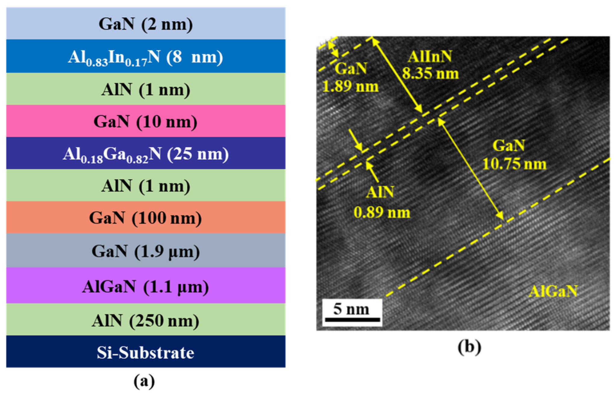
2. Materials and Growth Methods

The double channel epitaxial layers for fabricating AlInN/GaN/AlGaN/GaN MOSHEMTs were grown on a silicon (Si) substrate by metal-organic chemical vapor deposition (MOCVD, AIXTRON Group, Herzogenrath, Germany). Trimethylgallium (TMG), triethylgallium (TEG), trimethylaluminum (TMA), trimethylindium (TMI), and ammonia (NH3) were the precursors. Hydrogen and nitrogen were used as the carrier gases. The designed epitaxial layers, illustrated in Figure 1a, consisted of an AlN nucleation layer (250 nm), a step-graded AlGaN buffer layer (1.1 μm), an undoped GaN buffer layer (1.9 μm), a GaN channel 1 layer (100 nm), an AlN spacer layer (1 nm), an Al0.18Ga0.82N barrier 1 layer (25 nm), a GaN channel 2 layer (10 nm), an AlN spacer layer (1 nm), an Al0.83In0.17N barrier 2 layer (8 nm), and a GaN cap layer (2 nm). The AlN and AlGaN layers were grown at 1040–1100 °C in hydrogen ambient using TMG, while the Al0.83In0.17N layer was grown at 765 °C in nitrogen ambient using TEG in order to incorporate enough indium to the layer so as to achieve the same lattice constant as GaN’s. From the high-resolution transmission electron microscopy (HRTEM) image (JEOL Ltd., Tokyo, Japan) depicted in Figure 1b, the growth thicknesses of the epitaxial layers were similar with the designed thicknesses. Furthermore, as observed in Figure 1b, the channel region shows good matching with low dislocation density. Using a 1-dimensional (1D) Schrödinger-Poisson solver, the simulated band diagram and electron concentration distribution of the epitaxial layers are depicted in Figure 2. The simulation showed that double 2-DEG channels were constructed by the induced polarization in Al0.18Ga0.82N/GaN interface (channel 1) and the band discontinuity in lattice-matched Al0.83In0.17N/GaN interface (channel 2). Electron mobility of 1770 cm2/V-s and sheet electron density of 1.11 × 1013 cm−2 in the double channels were obtained using Hall measurement (Ecopia Corp., Anyang, South Korea)at room temperature.

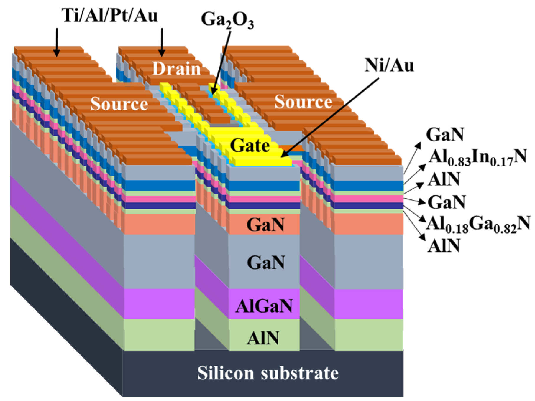
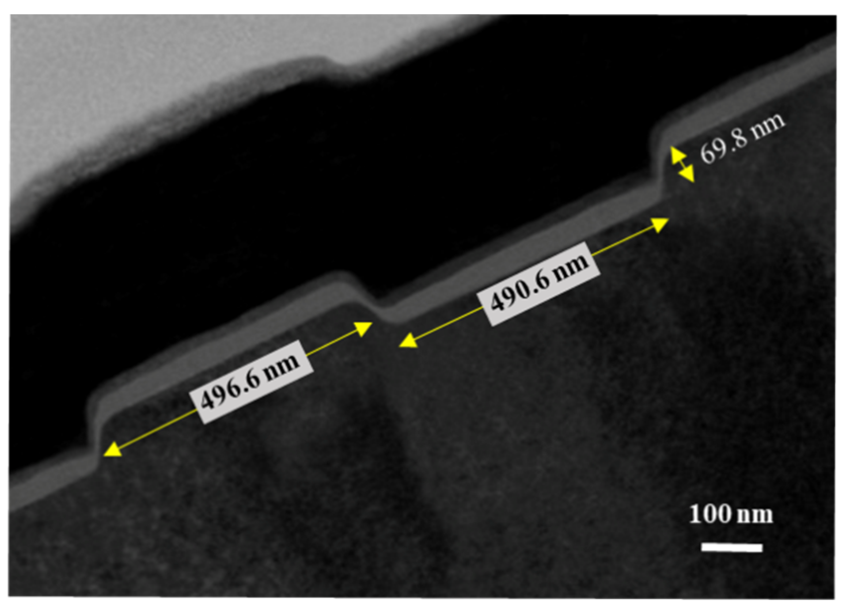
3. Device Fabrication

Figure 3 illustrates the 3-dimensional schematic configuration of the studied devices. Prior to patterning strip channel array as multiple-mesa-fin-channels using a He-Cd laser interference photolithography system, the fabrication processes of the devices started with a spread of photoresist AZ6112 on the sample. By adjusting the incident angle of the two-intersected He–Cd laser beams, 500-nm-wide strip channel arrays were patterned. Using a developer to remove the He–Cd laser illuminated photoresist, the patterned photoresist strip channel array was obtained. After depositing laminated metals of Ni/Au (20/100 nm) with an electron-beam evaporator, the Ni/Au metal mask was formed by lifting off the remaining Ni–Au metals above the photoresist strip channels. To fabricate the multiple-mesa channel, the unmasked region of the sample was etched down to the GaN buffer layer using a photoelectrochemical (PEC) etching method. The etching process and technology of the PEC etching method were demonstrated and reported previously [17]. Under a patterned Ni metal mask (500 nm), the mesa isolation region with an area of 310 μm × 320 μm was formed by etching down to the Si substrate using BCl3 etchant in a reactive-ion etching system. To completely remove the undesired native oxide residing on the surface of GaN cap layer, the sample was then surface-treated using an (NH4)2Sx chemical solution at 60 °C for 30 min. The (NH4)2Sx surface-treatment method was previously demonstrated and reported [18]. The source electrode and drain electrode of Ti/Al/Pt/Au (25/100/50/300 nm) laminated multiple metals were deposited using an electron-beam evaporator and then thermally annealed in a rapid-thermal-annealing system under a nitrogen atmosphere at 850 °C for 1 min. The separation between source electrode and drain electrode was approximately 10 μm. Prior to using a vapor cooling condensation system to deposit a 30 nm thick Ga2O3 gate oxide layer at approximately 80 K under liquid nitrogen cooling, the surface-treatment technique of a (NH4)2Sx chemical solution was utilized to treat the sample again. The deposition processes and performance of Ga2O3 films deposited by the vapor cooling condensation system were previously demonstrated and reported [19,20]. Using a standard photolithography method to pattern two-finger gate regions, Ni/Au (20/300 nm) gate laminated metals were deposited using the electron-beam evaporator, and the two-finger Ni/Au gate metals were manufactured using a lift-off process. Gate width and length were 50 and 1 μm, respectively. Furthermore, Ni/Au gate metals were placed in the central regions between source electrode and drain electrode.

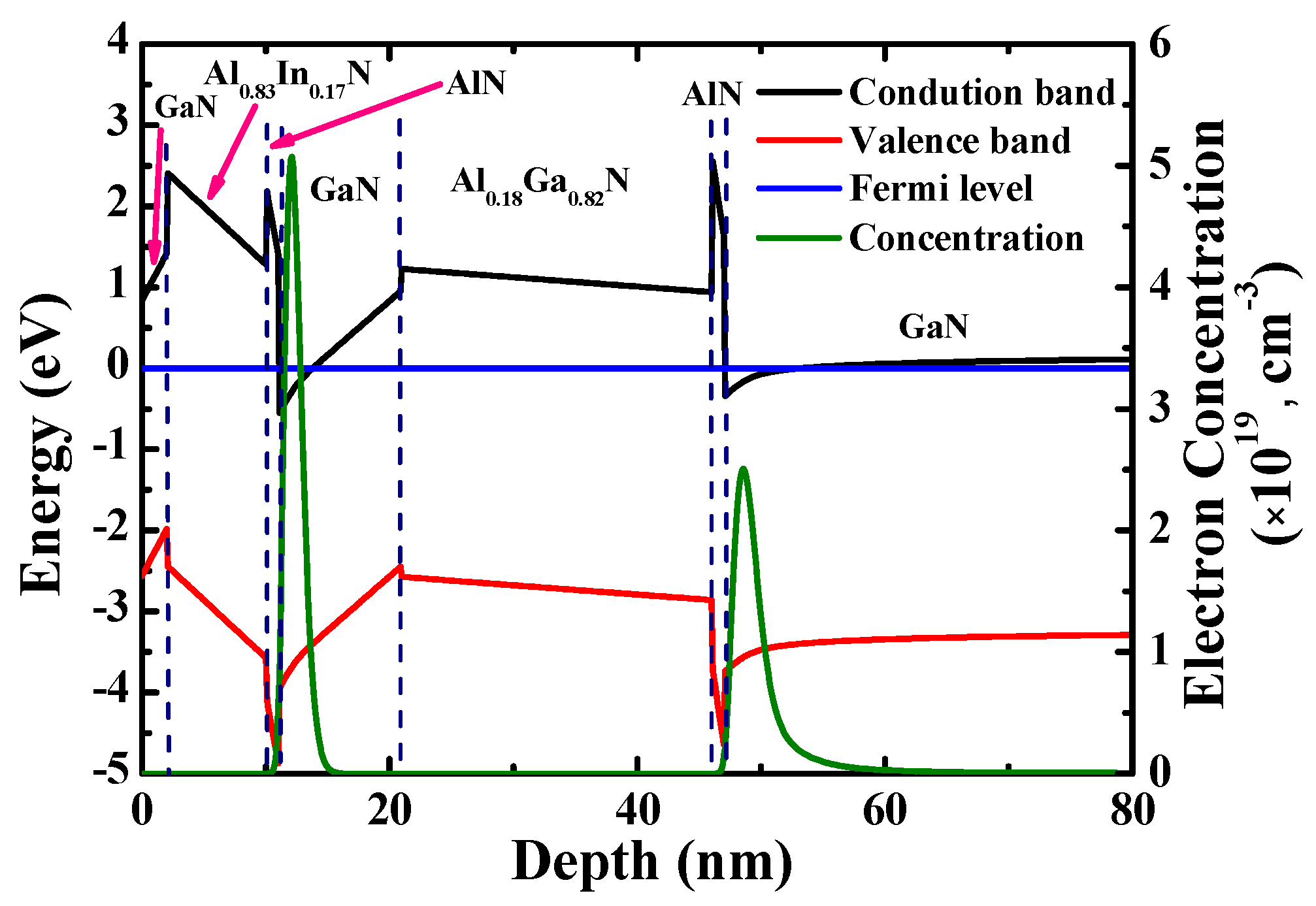
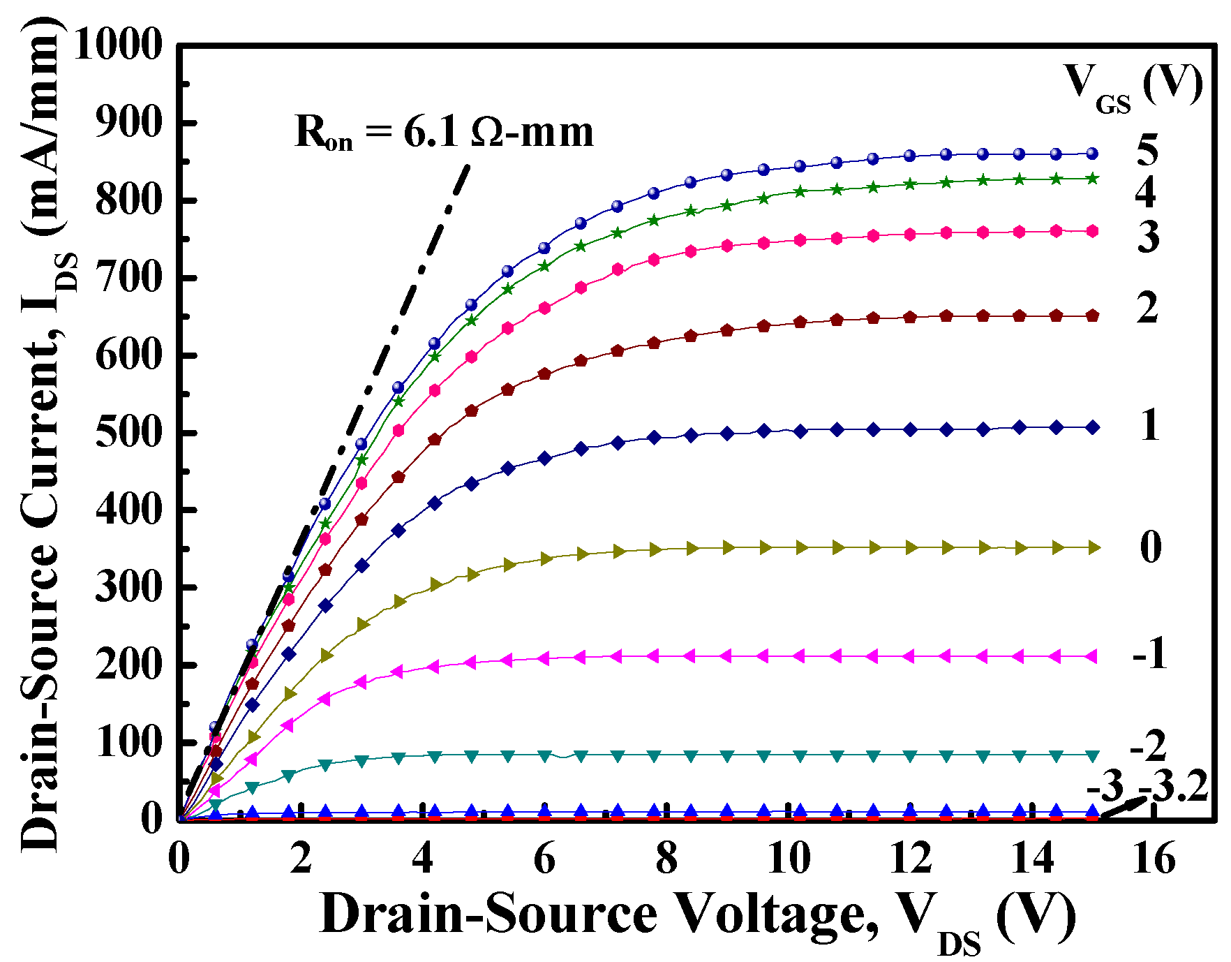
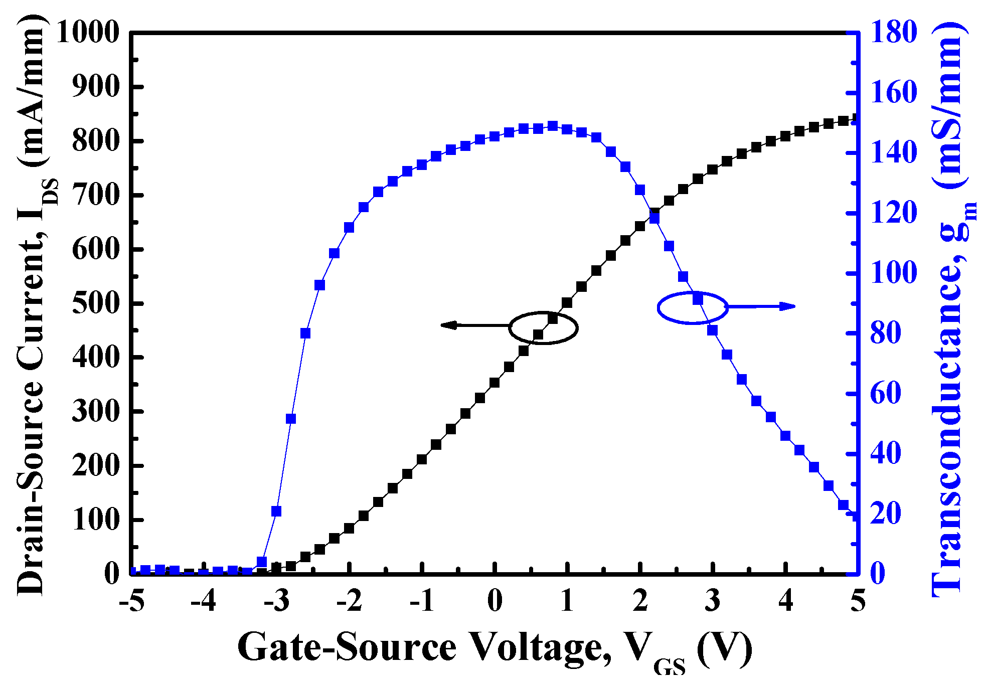
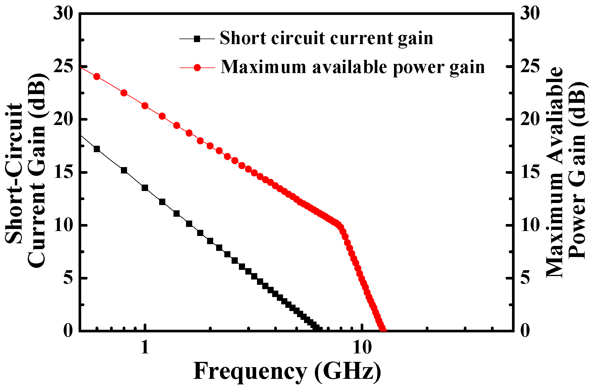
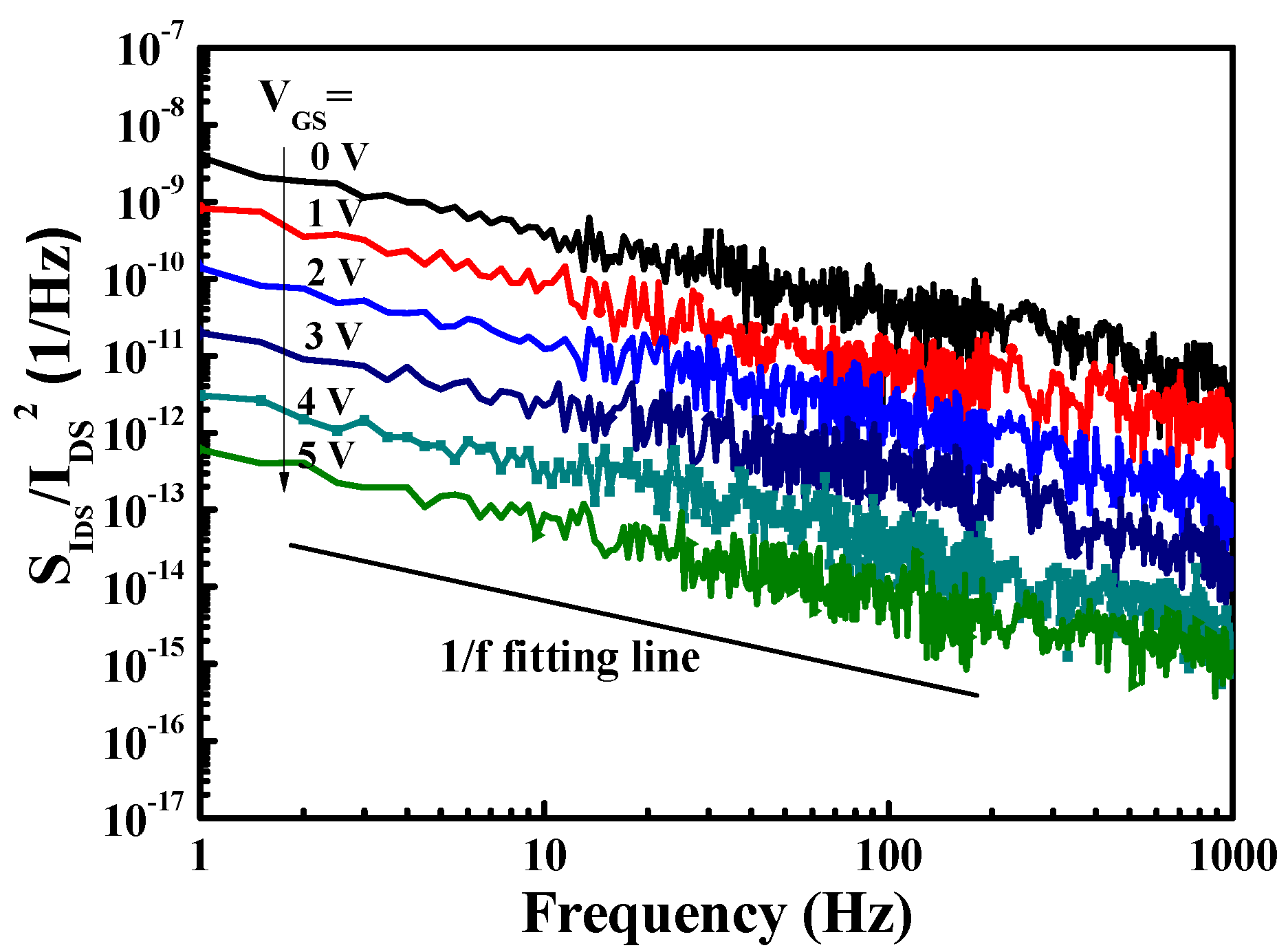
4. Results and Discussion

Figure 4 depicts the HRTEM image of the fin-channel. From the observation of HRTEM image, the height, width, and spacing of the multiple-mesa-channel were 69.8 nm, 496.6 nm, and 490.6 nm, respectively. Consequently, the total real channel width within a 50-μm-wide gate region was about 25.2 μm. By applying various gate-source voltage (VGS) levels, typical drain-source current (IDS)–drain-source voltage (VDS) characteristics of the studied devices, shown in Figure 5, were obtained using the measurement of an Agilent 4156C semiconductor parameter analyzer. Under the operating voltage of VDS= 10 V, its normalized saturation drain-source current was 352.0 and 842.7 mA/mm of the devices at VGS = 0 V and 5 V, respectively. At the operating voltage of VDS = 10 V, the dependence of drain-source current and extrinsic transconductance (gm) on gate-source voltage are depicted in Figure 6. Maximal extrinsic transconductance was 148.9 mS/mm. In general, the double-hump transconductance behaviors were caused by the effective gate modulation of the upper and lower channels in the double-channel MOSHEMTs, respectively [8,9,10]. However, double-hump transconductance characteristics did not appear in the gm–VGS curve of the studied devices. In the studied devices, the wider smooth gm value distribution caused by the collapse paving of double-hump transconductance behavior was contributed to the superior gate control of fin-channel. The superior gate control was attributed to the side-wall electric field modulation in the fin channel. By defining the on-resistance (Ron) as the inverse slope of the IDS–VDS characteristics at VGS = 5 V and VDS = 0 V, the associated on-resistance of 6.1 Ω-mm was obtained. Furthermore, when threshold voltage (Vth) was defined as the gate-source voltage corresponding to the drain-source current of 1 μA/mm, Vth was −3.2 V. To measure high-frequency performance of the studied devices using an Agilent 8510C network analyzer, Figure 7 illustrates the small-signal high-frequency performance of frequency-dependent short-circuit current gain and maximal available power gain. Figure 7 shows that the unit gain cutoff frequency (fT) and maximal oscillation frequency (fmax) were 6.5 and 12.6 GHz, respectively. In general, to evaluate electron trapping and electron detrapping behaviors induced from defects, traps, and interface states residing in electronic devices, the measurement of low-frequency noise performance was effective [21]. Under the operation of VDS = 1 V, Figure 8 depicts the frequency (f)-dependent normalized noise power density spectra ( S I DS ( f ) / I DS 2 ) of the studied devices measured by an Agilent 4156C semiconductor analyzer, an HP 35670A dynamic signal analyzer, and a BTA 9812B noise analyzer. The normalized noise power density gradually decreased with an increase in gate-source voltage. Due to the quite good variation between normalized noise power density and 1/f, flicker noise was the dominant noise of the devices. At the operating condition of f = 10 Hz, VDS = 1 V, and VGS = 5 V, the normalized noise power density was approximately 8.7 × 10⁻¹⁴ Hz−1. Using a mobility fluctuation model [22], Hooge’s coefficient α, a useful figure-of-merit parameter, could be expressed as:
α = ( S I DS ( f ) / I DS 2 ) · f · ( L G W G n ch ( V GS V th ) / | V th | )
where LG =1 μm and WG = 25.2 μm are the gate length and real gate width on multiple-mesa-fin-channels, respectively. The nch = 1.11 × 1013 cm−2 is the sheet electron density of the double-channel and Vth = −3.2 V is the threshold voltage. By substituting those parameters into Equation. 1, the α value of 6.25 × 10⁻⁶ was calculated for devices operating at f = 10 Hz, VDS = 1 V, and VGS = 5 V.

5. Conclusions

In this work, a MOCVD system was utilized to grow Al0.83In0.17N/GaN/Al0.18Ga0.82N/GaN heterostructured-epitaxial layers on Si substrates. According to the simulated energy band structure, polarization in Al0.18Ga0.82N/GaN interface and the band discontinuity in lattice-matched Al0.83In0.17N/GaN interface induced channels 1 and 2, respectively. The resulting double-channel epitaxial layers and multiple-mesa-fin-channel array were utilized for fabricating MOSHEMTs. Benefittig from the better gate control capability caused by the modulation of side-wall electrical field in fin-channel, the double-hump transconductance behavior, which occurred in double-channel MOSHEMTs, was not obtained. The multiple-mesa-fin-channel array used in double-channel MOSHEMTs could effectively pave the collapse of transconductance due to their better gate control capability. Owing to the high-insulating Ga2O3 gate oxide layer deposited by the vapor cooling condensation system and the inherent high-quality interface between the Ga2O3 and GaN layers, the low-flicker-noise performance was achieved. Under the operation of f = 10 Hz, VGS = 5 V, and VDS = 1 V, the low Hooge’s coefficient α was approximately 6.25 × 10⁻⁶.

Author Contributions

Conceptualization, C.-T.L.; data curation, H.-Y.L. and D.-S.L.; software and epitaxial growth, J.-I.C.; funding acquisition, C.-T.L.; investigation, H.-Y.L., E.Y.C. and C.-T.L.; writing–original draft, C.-T.L.; writing–review and editing, H.-Y.L. and C.-T.L. All authors have read and agreed to the published version of the manuscript.

Funding

This research was funded by the Ministry of Science and Technology of Taiwan under the grant of MOST-108-2221-E-006-215-MY3, MOST 108-2221-E-155-029-MY3, and MOST 109-2923-E-155-001.

Institutional Review Board Statement

Not applicable.

Informed Consent Statement

Not applicable.

Data Availability Statement

The data presented in this study are available on request from the corresponding author.

Acknowledgments

The authors would appreciate the financial support from the Ministry of Science and Technology of the Republic of China.

Conflicts of Interest

The authors declare no conflict of interest.

References

  1. Chiou, Y.L.; Lee, C.T. Band alignment and performance improvement mechanisms of chlorine-treated ZnO-gate AlGaN/GaN metal–oxide–semiconductor high-electron mobility transistors. IEEE Trans. Electron Devices 2011, 58, 3869–3875. [Google Scholar] [CrossRef]
  2. Shi, J.L.; Eastman, F.; Xin, X.; Pophristic, M. High performance AlGaN/GaN power switch with HfO2 insulation. Appl. Phys. Lett. 2009, 5, 042103. [Google Scholar] [CrossRef]
  3. Lee, C.T.; Yang, C.L.; Tseng, C.Y.; Chang, J.H.; Horng, R.H. GaN-based enhancement-mode metal-oxide-semiconductor high-electron mobility transistors using LiNbO3 ferroelectric insulator on gate-recessed structure. IEEE Trans. Electron Devices 2015, 62, 2481–2487. [Google Scholar] [CrossRef]
  4. Roccaforte, F.; Greco, G.; Fiorenza, P.; Iucolano, F. An overview of normally-off GaN-based high electron mobility transistors. Materials 2019, 12, 1599. [Google Scholar] [CrossRef] [Green Version]
  5. Lim, T.; Aidam, R.; Waltereit, P.; Henkel, T.; Quay, R.; Lozar, R.; Maier, T.; Kirste, L.; Ambacher, O. GaN-based submicrometer HEMTs with lattice-matched InAlGaN barrier grown by MBE. IEEE Electron Device Lett. 2010, 31, 671–673. [Google Scholar] [CrossRef]
  6. Ma, J.; Lu, X.; Zhu, X.; Huang, T.; Jiang, H.; Xu, P.; Lau, K.M. MOVPE growth of in situ SiNx/AlN/GaN MISHEMTs with low leakage current and high on/off current ratio. J. Cryst. Growth 2015, 414, 237–242. [Google Scholar] [CrossRef]
  7. Jha, S.K.; Surya, C.; Chen, K.J.; Lau, K.M.; Jelencovic, E. Low-frequency noise properties of double channel AlGaN/GaN HEMTs. Solid-State Electron. 2008, 52, 606–611. [Google Scholar] [CrossRef]
  8. Kamath, A.; Patil, T.; Adari, R.; Bhattacharya, I.; Ganguly, S.; Aldhaheri, R.W.; Hussain, M.A.; Saha, D. Double-channel AlGaN/GaN high electron mobility transistor with back barriers. IEEE Electron Device Lett. 2012, 33, 1690–1692. [Google Scholar] [CrossRef]
  9. Chu, R.; Zhou, Y.; Liu, J.; Wang, D.; Chen, K.J.; Lau, K.M. AlGaN-GaN double-channel HEMTs. IEEE Trans. Electron Devices 2005, 52, 438–446. [Google Scholar] [CrossRef]
  10. Wei, J.; Liu, S.; Li, B.; Tang, X.; Lu, Y.; Liu, C.; Hua, M.; Zhang, Z.; Tang, G.; Chen, K.J. Low on-resistance normally-off GaN double-channel metal–oxide–semiconductor high-electron-mobility transistor. IEEE Electron Device Lett. 2015, 36, 1287–1290. [Google Scholar] [CrossRef]
  11. Ohi, K.; Asubar, J.T.; Nishiguchi, K.; Hashizume, T. Current stability in multi-mesa-channel AlGaN/GaN HEMTs. IEEE Trans. Electron Devices 2013, 60, 2997–3004. [Google Scholar] [CrossRef] [Green Version]
  12. Lu, B.; Matioli, E.; Palacios, T. Tri-gate normally-off GaN power MISFET. IEEE Electron Device Lett. 2012, 33, 360–362. [Google Scholar] [CrossRef]
  13. Jia, J.J.; Lin, C.C.; Lee, C.T. Scaling effect in gate-recessed AlGaN/GaN fin-nanochannel array MOSHEMTs. IEEE Access 2020, 8, 158941–158946. [Google Scholar] [CrossRef]
  14. Pearton, S.J.; Yang, J.; Cary IV, P.H.; Ren, F.; Kim, J.; Tadjer, M.J.; Mastro, M.A. A review of Ga2O3 materials, processing, and devices. Appl. Phys. Rev. 2018, 5, 011301. [Google Scholar] [CrossRef] [Green Version]
  15. Stepanov, S.I.; Nikolaev, V.I.; Bougrov, V.E.; Romanov, A.E. Gallium oxide: Properties and application-a review. Rev. Adv. Mater. Sci. 2016, 44, 63–86. [Google Scholar]
  16. Chen, K.J.; Yang, S.; Tang, Z.; Huang, S.; Lu, Y.; Jiang, Q.; Liu, S.; Liu, C.; Li, B. Surface nitridation for improved dielectric/III-nitride interfaces in GaN MIS-HEMTs. Phys. Status Solidi A 2015, 212, 1059–1065. [Google Scholar] [CrossRef]
  17. Chiou, Y.L.; Lee, C.S.; Lee, C.T. Frequency and noise performances of photoelectrochemically etched and oxidized gate-recessed AlGaN/GaN MOS-HEMTs. J. Electrochemi. Soc. 2011, 158, H477–H481. [Google Scholar] [CrossRef]
  18. Chiou, Y.L.; Lee, C.S.; Lee, C.T. AlGaN/GaN metal-oxide-semiconductor high-electron mobility transistors with ZnO gate layer and (NH4)2Sx surface treatment. Appl. Phys. Lett. 2010, 97, 032107. [Google Scholar] [CrossRef]
  19. Jian, L.Y.; Lee, H.Y.; Lee, C.T. Ga2O3-based p-i-n solar blind deep ultraviolet photodetectors. J. Mater. Sci.-Mater. Electron. 2019, 30, 8445–8448. [Google Scholar] [CrossRef]
  20. Lee, H.Y.; Chang, T.W.; Lee, C.T. AlGaN/GaN metal-oxide-semiconductor high-electron mobility transistors using Ga2O3 gate dielectric layer grown by vapor cooling condensation system. J. Electron. Mater. 2021, 50, 3748–3753. [Google Scholar] [CrossRef]
  21. Levinshtein, M.E.; Rumyantsev, S.L.; Gaska, R.; Yang, J.W.; Shur, M.S. AlGaN/GaN high electron mobility field effect transistors with low 1/f noise. Appl. Phys. Lett. 1998, 73, 1089–1091. [Google Scholar] [CrossRef]
  22. Hooge, F.N.; Kleinpenning, T.G.M.; Vandamme, L.K.J. Experimental studies on 1/f noise. Rep. Prog. Phys. 1981, 44, 479–532. [Google Scholar] [CrossRef]
Figure 1. (a) Schematic structure and (b) high-resolution transmission electron microscopy image of epitaxial layers.
Materials 14 05474 g001
Figure 2. Simulated band diagram and electron concentration distribution in epitaxial layers.
Materials 14 05474 g002
Figure 3. Three-dimensional schematic configuration of MOSHEMTs with multiple-mesa-fin-channel array.
Materials 14 05474 g003
Figure 4. High resolution transmission electron microscope image of cross-sectional fin-channel.
Materials 14 05474 g004
Figure 5. Typical drain−source current−drain−source voltage characteristics of MOSHEMTs with multiple-mesa-fin-channel array.
Materials 14 05474 g005
Figure 6. Under the operation of drain−source voltage of 10 V, drain−source current and extrinsic transconductance as a function of gate−source voltage of MOSHEMTs with multiple-mesa-fin-channel array.
Materials 14 05474 g006
Figure 7. Short-circuit current gain and maximum available power gain as a function of frequency of MOSHEMTs with multiple-mesa-fin-channel array.
Materials 14 05474 g007
Figure 8. Under drain−source voltage of 1 V, frequency-dependent normalized noise power spectra of MOSHEMTs with multiple-mesa-fin-channel array.
Materials 14 05474 g008
Publisher’s Note: MDPI stays neutral with regard to jurisdictional claims in published maps and institutional affiliations.

