Article

Synthesis of Copper Nitride Layers by the Pulsed Magnetron Sputtering Method Carried out under Various Operating Conditions

by
Magdalena Wilczopolska
1,*,
Katarzyna Nowakowska-Langier
1,*,
Sebastian Okrasa
1,
Lukasz Skowronski
2,
Roman Minikayev
3,
Grzegorz W. Strzelecki
1,
Rafal Chodun
4 and
Krzysztof Zdunek
4
1
National Centre for Nuclear Research, Material Physics Department, Plasma/Ion Beam Technology Division, 05-400 Otwock, Poland
2
Institute of Mathematics and Physics, UTP University of Science and Technology in Bydgoszcz, 85-796 Bydgoszcz, Poland
3
Laboratory of X-ray and Electron Microscopy Research, Institute of Physics PAS, Polish Academy of Sciences, 02-668 Warsaw, Poland
4
Division of Surface Engineering, Faculty of Materials Science and Engineering, Warsaw University of Technology, 00-661 Warsaw, Poland
*
Authors to whom correspondence should be addressed.
Materials 2021, 14(10), 2694; https://doi.org/10.3390/ma14102694
Submission received: 29 March 2021 / Revised: 12 May 2021 / Accepted: 17 May 2021 / Published: 20 May 2021
(This article belongs to the Special Issue Optical Characterization and Applications of Metallic Thin Films)

Abstract

:
Copper nitride shows various properties that depend on the structure of the material and is influenced by the change in technical parameters. In the present work, Cu–N layers were synthesized using the pulsed magnetron sputtering method. The synthesis was performed under different operating conditions: direct current (DC) or alternating current (AC) power supply, and various atmospheres: pure Ar and a mixture of Ar + N2. The structural properties of the deposited layers were characterized by X-ray diffraction measurements, and Raman spectroscopy and scanning electron microscopy have been performed. Optical properties were also evaluated. The obtained layers showed tightly packed columnar grain features. The kinetics of the layer growth in the AC mode was lower than that observed in the DC mode, and the layers were thinner and more fine-grained. The copper nitride layers were characterized by the one-phase and two-phase polycrystalline structure of the Cu3N phase with the preferred growth orientation (100). The lattice constant oscillates between 3.808 and 3.815 Å for one-phase and has a value of 3.828 Å for a two-phase structure. Phase composition results were correlated with Raman spectroscopy measurements. Raman spectra exhibited a broad, diffused, and intense signal of Cu3N phase, with Raman shift located at 628–635 cm−1. Studies on optical properties showed that the energy gap ranged from 2.17 to 2.47 eV. The results showed that controlling technical parameters gives a possibility to optimize the structure and phase composition of deposited layers. The reported changes were discussed and attributed to the properties of the material layers and technology method.

1. Introduction

Copper nitride (Cu3N) layers exhibit promising physical properties, can be synthesized economically, and are nontoxic and highly stable, but only under room temperature. Their lattice constant often changes according to the production techniques. Therefore, an interesting feature of this material is that depending on the stoichiometry (lattice constant parameter) of the obtained Cu3N compound, it may exhibit properties typical of an insulator [1] or a semiconductor [1,2,3,4], and even those properties that are characteristically shown by a conductive material [5].
Successful synthesis of Cu3N is associated with difficulties related primarily to the narrow range of thermodynamic stability of the Cu3N phase, which decomposes at a high temperature. Large discrepancies are observed in terms of the decomposition temperature. According to previous studies [6,7,8], the decomposition temperature ranges from 100 to 450 °C. The reported differences are most likely related to the conditions of synthesis that determine the final structure of the material. It is known that in Cu3N synthesized using glow discharge with a magnetic field, the degree of material defects most likely affects the thermodynamic stability of the material. The range of thermodynamic stability of this material corresponds to the characteristic temperature of the I zone of the structural models [9]; low temperature during the synthesis and limited surface diffusion leads to an unfavorable structure of the material (defects and columnar structure). Heat activation, which results in synthesis, is hindered by the thermodynamic stability of the material. The practical range of synthesis of such materials is very narrow and difficult to observe. On the basis of our previous studies [10,11,12], plasma surface engineering could be used to synthesize the metastable Cu3N material with reduced thermal activation. In the pulsed magnetron sputtering (PMS) method, the synthesis process is implemented in a pulsed manner, which enables it to be substituted for different forms of energy during synthesis. In addition, this method gives visibility to a greater degree of the parameters, such as electrical energy resulting from the participation of energetic species and electric field during the process of synthesis, which means a non-equilibrium plasma state.
The main objective of the present paper was focused on the technology of copper nitride layers synthesis, i.e., change of the technological parameters, such as working mode AC/DC of pulsed power supply and gas environment, to obtain structure and optimization of deposition processes in terms of the desired quality of the obtained material. Production of high-quality material with a single-phase Cu3N structure is important from the point of view of, firstly, the verification of the adopted hypothesis regarding the scope of possibilities of searching for other synthetic pathways, and secondly, it opens up new application perspectives by using the base material with a stabilized phase composition.

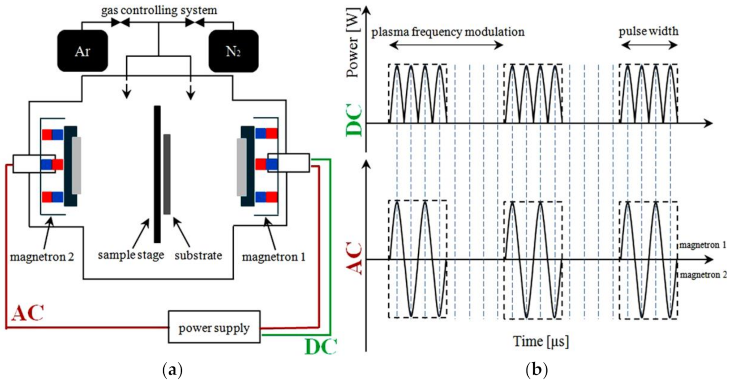
2. Materials and Methods

The material was synthesized using the PMS method. Cu3N layers were synthesized by the circular magnetron WMK-50 (IMT, Wroclaw University of Technology, Poland) (according to the Gencoa classification of balanced/unbalanced magnetrons where distance to the null point (ZBZ) is 28 mm, g = 1.27 [13,14,15]). A 50-mm diameter and a 6-mm thick copper target (Grade 1 purity) was used as a magnetron cathode. This method enabled the material to be synthesized on a cold surface. Moreover, there was no risk of thermal decomposition of the Cu–N layer.
The magnetron cathode was powered by a 10 kW DORA PS pulsed power supply [16,17], operated in two modes: DC and AC [18,19]. This device controls the modulation of carrier frequency [20]. Figure 1 shows a schematic illustration of the experimental setup and operation of the power supply system. The schematic overview in Figure 1b shows the differences in the operation of the power supply system in AC and DC modes. The figure illustrates the plasma pack generation controlled by pulsed width modulation.
The DORA PS power supply could operate in both AC and DC modes. The AC mode is provided by a super-modulated sine wave with 50% duty cycle. In the DC mode, the negative half-periods of the signal are transferred to the positive side of the waveform. In the AC mode, the two magnetrons were working alternately (the magnetrons were mounted in the chamber in mirror configuration, but only one magnetron was used during the experiment to synthesize our samples). This implies that only the positive part of the AC waveform was involved in plasma generation. Thus, the plasma contribution in the bipolar process of film synthesis was half of that of the unipolar process. The ability to work in these two modes reduced the share in the synthesis of plasma, which implies that the life span of plasma was shortened by half, while retaining the other synthesis parameters at the same level.
Cu3N layers were deposited on non-heated Si (100) (Lukasiewicz Research Network—Institute of Electronic Materials Technology, Warsaw, Poland), and glass substrates (SIMAX, Blachownia, Poland) by the PMS method [16]. The substrates were ultrasonically cleaned (Codyson 0,6l 50W CD3800, Shenzhen Codyson Electrical Co., Guangdong, China) in acetone (Linegal Chemicals, Warsaw, Poland) and mounted on a stage located at a distance of dS-T = 10 cm from the magnetron cathode. The substrate surface was oriented perpendicularly to the Z-axis of the magnetron cathode. During insertion of the substrate, the chamber is opened and the target is exposed to impurities that can get onto its surface. In order to remove contaminants from the target pre-sputtering processes are carried out. A cathodic material was pre-sputtered in a 1.2 Pa argon atmosphere for 10 min before every layer deposition process.
Cu3N layers were fabricated in four variants: DC and AC power supply modes and various gas atmospheres. The copper cathode was sputtered with 80 W power in an atmosphere of pure nitrogen (N2) and its mixture with argon (N2 + Ar). For AC processes, the sputtering time was extended to twice the normal time because the generation time of plasma was reduced by half (Figure 1). The time of sputtering was set to 60 and 120 min for DC and AC modes, respectively, to compare the deposited layers (Table 1).
The surface of the deposited layers was characterized by scanning electron microscopy (SEM, Zeiss, Jena, Germany). The chemical composition (at.%) of the Cu–N layers was analyzed by an energy-dispersive X-ray (EDS) analyzer (SEM, Zeiss, Jena, Germany), 20 kV, working distance 10 cm). The phase composition of the Cu–N layers was analyzed by an X-ray diffraction technique, with help of an laboratory diffractometer X’Pert Pro Alpha1 MPD (XRD, Malvern-Panalitical, Almelo, Netherlands) equipped with Cu-Kα X-ray tube. The layers were measured in the 2θ scan mode. To confirm phase composition, oscillation spectroscopy was performed using a Raman Jasco NRS 5100 spectrometer (Jasco, Tokyo, Tokyo Metropolitan Prefecture, Japan) operating in backscatter geometry and using 532 nm argon ion laser.
Optical studies of the Cu–N layers on silicon and glass substrates were performed by spectroscopic ellipsometry (a rotating analyzer device: V-VASE device, J.A. Woollam Co., Inc., Lincoln, NE, USA) and spectrophotometry (a Cary 5000 unit, Agilent, Santa Clara, CA, USA). The ellipsometric parameters Ψ and Δ azimuths were recorded in the photon energy spectral range from 0.62 eV (2000 nm) to 5 eV (248 nm), with a resolution of 0.02 eV for three angles of incidence (65°, 70°, and 75°). Transmittance spectra (T) were acquired for a near-normal incidence of light for the wavelength region from 248 nm to 2000 nm (the resolution for this measurement was 2 nm). These measurements allowed us to obtain refractive index (n) and extinction coefficient (k). The optical band gap energy was obtained by extrapolating the absorption edge line with abscissa to the low energy.

3. Results

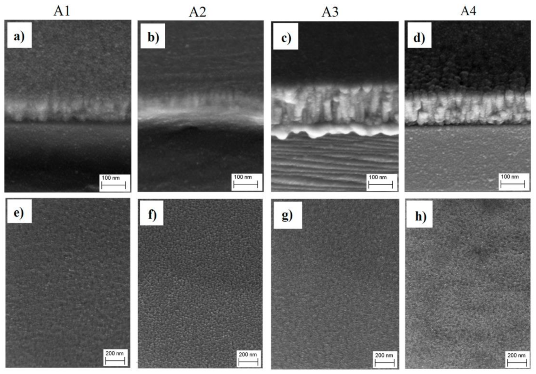
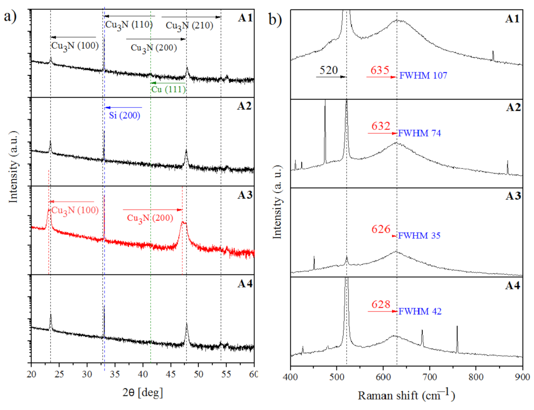
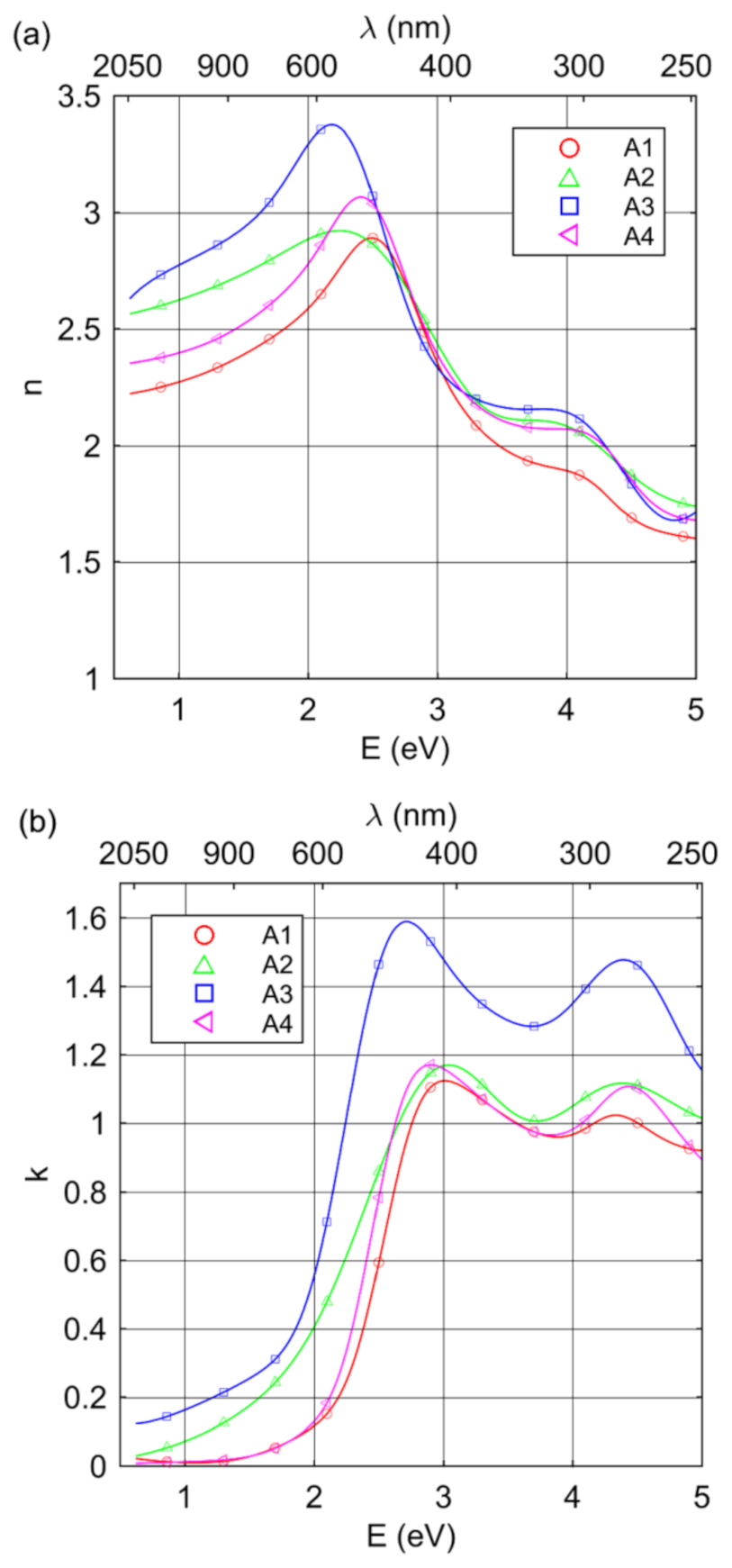
3.1. Structure and Phase Composition of Copper Nitride

Figure 2 shows cross-section and surface morphology images of the Cu–N layers prepared with various process parameters. In terms of morphology, the obtained layers showed tightly packed columnar grains features and sharp grain boundaries; this characteristic is commonly observed in layers obtained by magnetron sputtering and agrees well with the zone transition (T) microstructure of Thornton’s model [9]. All the layers showed clean and smooth surface morphology. The working mode (AC or DC) had more influence on the morphology and structure of the layer than the plasma working gases. The kinetics of the layer growth in the AC mode, despite the use of a longer time (to compensate for the loss of plasma generation to the second magnetron), were lower than that observed in the DC mode. The AC mode caused the layers to be thinner and more fine-grained than those obtained in the DC mode [21].
Figure 3a shows the X-ray diffraction patterns of the Cu–N layers. The obtained Cu–N layers had an anti-ReO3 polycrystalline structure with a privileged orientation, with the preferred growth orientation along the direction (100) (Figure 3). Diffraction studies enabled the calculation of the lattice constant. The three layers that met the requirements of a single-phase structure showed results similar to the literature data on the Cu3N phase [17]. The lattice parameter (a0) of the synthesized layers was calculated from the X-ray peak position of the lattice plane reflex (hkl), and it was found to oscillate between 3.808 and 3.815 Å, according to the values from the literature for stoichiometric single crystal Cu3N = 3.815 Å [2,22,23]. Bragg peaks corresponded to the Cu3N crystalline structure. In addition, a Cu(111) reflection of the Cu capping layer was observed. The mean grain size of the layers was estimated by the Scherrer formula, and the results are presented in Table 2. These layers are stoichiometric, single phase, with similar grain size values of 30–35 nm. However, a two-phase structure was obtained for one of the layers. The peaks recorded on the diffractogram corresponded to two polycrystalline phases that crystallized in the structure of the ReO3-copper nitride type, but with different stoichiometries. One of them corresponded to the phase of stoichiometric copper nitride with a small crystallite size of 15 nm. For the second phase, the peaks shifted to the lower values of the angle 2θ, which corresponded to Cu3N supersaturated with copper (Cu) (Figure 3a). This phase had a larger lattice constant of 3.828 Å and a bigger size of grains. The layer was probably stoichiometric with cubic Cu3N and regions of Cu3N saturated with copper; this is because when more Cu was interstitially doped, Cu3N was retained as a cubic structure with a larger lattice constant. In terms of the technical process, this is most likely due to the more intensive spraying of the copper target, along with energy conditions prevailing on the surface. The above discussion demonstrates that XRD diffraction patterns of Cu3N show no dependence on the structure of synthesized layers on various PMS process parameters.
Phase composition obtained through the X-ray diffraction method was confirmed by the results obtained from the Raman spectroscopy method. Figure 3b shows the obtained spectra recorded for the Cu–N layers. The crystal structure of Cu3N belongs to the space group, Pm-3m, wherein the unit cell contains one formula unit. The space group analysis predicts 12 phonon modes at Γ point, out of which nine optic modes with symmetry representation are as follows: Γ = 2F1u + F2u. The F1u modes are infrared (IR) active and F2u modes are optically inactive (silent mode). Hence, no first-order Raman signal is expected for a perfect cubic Cu3N. However, the experimental results available for Raman spectra of this material are quite debatable; they show the presence of Raman peak at 634 cm−l for Cu3N thin films [12,24,25,26,27]. Though the theoretical calculation inhibits the presence of Raman active modes for a perfect cubic Cu3N, the possibility of modes arising because of the selection rule break down due to non-stoichiometry cannot be ruled out. These modes arise because of the selection rule breakdown owing to the highly non-stoichiometric nature (due to the presence of defects and disorders at Cu and N sites) and multi-phonon combinations. Consideration of the results of Raman shift at 634 cm−1 for Cu3N films and XRD complement each other and confirm our predictions. However, a more detailed theoretical analysis dedicated to the exact assignment of Raman-active peak would be required for a proper interpretation.
Considering the above reasons, perfect copper nitride is very difficult to synthesize. However, based on literature data and other research methods, such as XRD and the examination of optical properties, we are confident that obtained layers are copper nitride. Raman shift around 635 cm−1 corresponds to copper nitride which, however, has no perfect cubic Cu3N lattice with the symmetry group (Pm-3m). The Raman shift located at 520 cm−1 originated from the silicon substrate on which the layer was synthesized. Raman spectra exhibited a broad, diffused, and intense fluorescence signal of Cu3N. The position of peaks and FWHM (full width at half maximum) and shape were optimized by the Voight function in OriginLab (OriginPro 7.5, OriginLab Corporation, Northampton, MA, USA). All results were fitted and are listed in Table 2. The results of Raman spectroscopy also showed a greater effect of the working mode (AC or DC) on the structure than the yield-generating gases. Considering the change in the working mode, the Raman shift of the layers deposited by the AC mode was similar to that found in the literature data. However, the spectrum obtained from the DC mode was not significantly different. This spectrum was shifted to lower wavenumbers. The FWHM values were dependent on the working mode and showed whether the layer was crystalline or amorphous. The Raman spectra of crystalline and amorphous solids of the same chemical composition can be significantly different, primarily because of the presence or absence of spatial order and long-range translational symmetry, respectively. Amorphous solids can be thought of as a collection of formula units of the same chemical composition, but with varying bond angles and lengths depending upon chemical bond interactions with their nearest neighbors. There is no order to their arrangement in space. Consequently, one does not observe the narrow bands. One can clearly observe that the FWHM results of Cu–N layers obtained by pulsed magnetron sputtering show wide bands, typical for amorphous layers. However, the value of FWHM of the layers obtained by the DC mode is significantly lower than from AC mode. It is known that widths depend upon the degree of chemical interaction between the molecules. Therefore, it can be assumed that working mode may impact the structure of copper nitride layers. Differences in Raman shifts in the results obtained by various PMS process parameters could be a reason for subtle structural changes. The Raman shift of the A1 sample at 635 cm−1 obtained under the AC mode and Ar + N2 gas atmosphere was consistent with the Cu3N peaks reported in the literature. The Raman spectra of the A3 sample did not clearly show any differences in the obtained results for the two-phase layer. This could be explained by the fact that the Raman laser spot diameter was 0.6 μm, and it was difficult to find areas with two phases when performing a measurement.

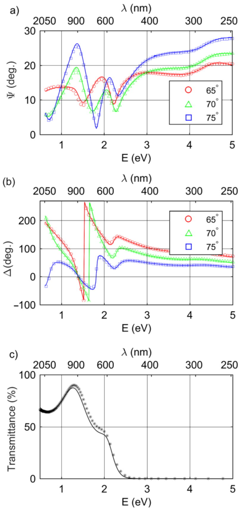
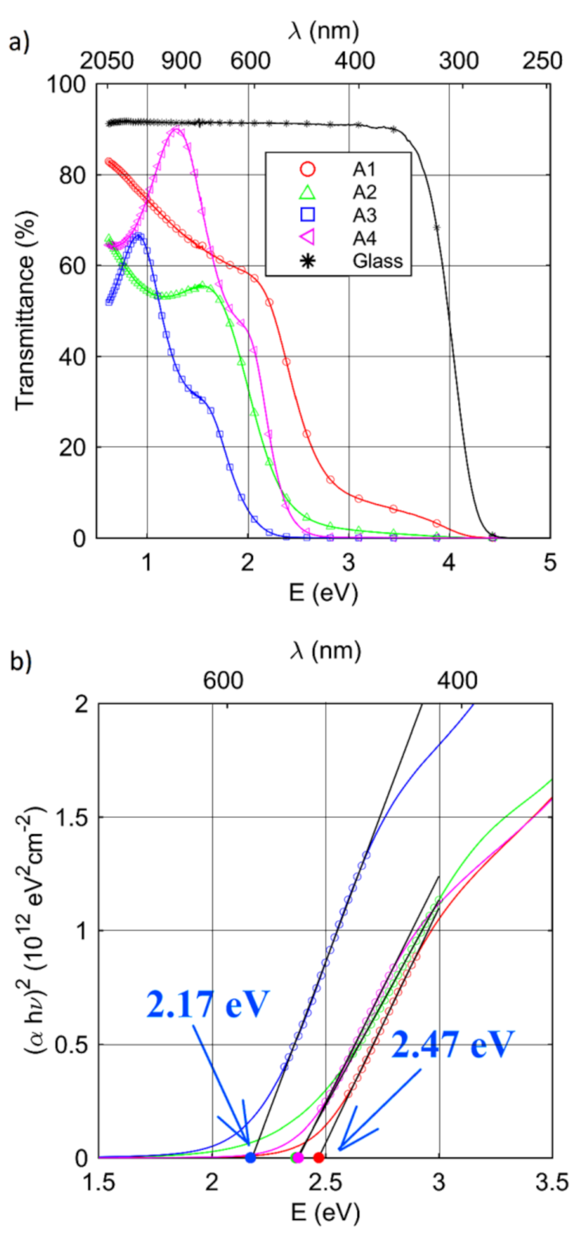
3.2. Optical Properties of the Cu3N Layers

Optical constants of the examined Cu3N coatings and the thicknesses of the Cu–N and rough layers were determined using a four-medium optical model of the sample (ambient/rough layer/Cu–N layer/glass substrate) by combining both ellipsometric (Ψ and Δ) and spectrophotometric (T) measurements. Optical constants of Cu–N were parameterized using sum Gaussian-( ε ˜ G ) and/or Lorentzian-type ( ε ˜ L ) oscillators [28,29], as well as PSEMI-M1 ( ε ˜ P S E M I ) shape of absorption line near the optical band gap [28]. Additionally, a Drude ( ε ˜ D ) term was considered. Generally, the complex dielectric function ( ε ˜ ) of the produced Cu–N layers can be written as follows:
ε ˜ = n + i k 2 = ε + ε ˜ D ω p , Γ + ε ˜ P S E M I A , E , B , W L , W R , A L , A R + j ε ˜ L , G A j , E j , B r j
where n is the real part of the complex refractive index, k is the extinction coefficient, ε is a high-frequency dielectric constant, and ω p   and Γ   are the plasma energy and free-carrier damping, respectively. In Equation (1), A/Aj is the amplitude, E/Ej is the energy of the absorption line, and Brj is the broadening of the oscillator. Parameters B, WL, WR, AL, and AR are associated with the broadening and shape of the PSEMI-M1 absorption line. The analytical formulas related to the particular oscillators are described in [28,29]. Optical constants of the substrate were taken from the database of optical constants [28]. Optical properties of the rough layer were described as a Bruggeman Effective Medium Approximation [28,29], with fractions of void and Cu–N equal to 50%. The parameters of particular absorption lines and thicknesses of the rough (dr) and Cu–N layers (dCu–N) were varied to minimize the reduced mean squared error ( χ 2 ) defined as [28,29]:
χ 2 = 1 N Ψ Δ P j Ψ j mod Ψ j exp σ j Ψ 2 + Δ j mod Δ j exp σ j Δ 2 + 1 N T P j T j mod T j exp w T σ j T 2
where N Ψ Δ , T and P are the total number of data points and the number of fitted model parameters, respectively. The variables with superscripts exp and mod correspond to the experimental and calculated data, respectively. In Equation (2), w T   is weighting of T values, while variables σ j Ψ , σ j Δ , and σ j T are standard deviations of Ψ, Δ, and T data, respectively. The procedure of fitting was performed using the WASE32 software (version 3.774, J.A. Woollam Co., Inc., Lincoln, NE, USA) [28]. An example of the fit (for sample A4) is presented in Figure 4.
Thicknesses of the Cu–N layers estimated during the analysis of spectroscopic ellipsometry combined with transmittance data summarized in Table 3 were in the range of approximately 80 nm (A1) to approximately 220 nm (A3). The thicknesses of the rough layers (2.9–9.7 nm; see Table 3) did not exceed 10% of the thickness of the Cu–N layers.
Figure 5 shows the real part of the complex refractive index and extinction coefficient of the synthesized Cu–N layers. In general, the shape of k with two maximums at 2.5–3.0 eV and 4.3 eV is typical for Cu–N layers and was reported earlier. In the IR spectral range, the extinction coefficient values were relatively small, especially for A1 and A4 samples. This behavior of k for long wavelengths was directly associated with the phase composition of Cu–N layers, particularly with the non-stoichiometry of Cu3N, or existence/coexistence of the pure Cu phase and/or the Cu3N phase supersaturated with Cu. The Drude term describes the interaction of electromagnetic radiation with free carriers. During the analysis of optical spectra, the Drude term was found only for samples produced under Ar + N2 mixture. For specimens deposited under pure N2 atmosphere, the plasma energy reached a value of zero during the fit procedure. The increase in k, with the increase in the wavelength (for λ > 1200 nm) for sample A1, and the relatively high value of k for sample A3, were associated with absorption caused by free carriers. The values of plasma energy were relatively small (0.27 and 0.58 eV for samples A1 and A3, respectively). The free carrier damping was 0.79 and 0.10 eV for samples A1 and A3, respectively; however, the uncertainty of the first value was high (approximately 50% of Γ ). On the basis of the estimated ω p and Γ values, the optical resistivity ( ρ o p t = Γ ε 0 ω p ; ε 0 –permittivity of vacuum) and mean relaxation time of free carriers ( τ = Γ 1 ) were calculated (Table 3). The values of ρ o p t   = 80 k Ω cm and τ = 0.8 fs for sample A1 were determined with high uncertainty (approximately 50%). The mean relaxation time of free carriers and optical resistivity for sample A3 were 6.4 fs and 2.3 k Ω cm, respectively. The conductivity of the Cu–N layers was associated with the insertion of Cu atoms into the body center of the Cu3N structure. This result agrees well with XRD measurement results, where, apart from the Cu3N structure, the Cu3N phase supersaturated with Cu was found.
Transmittance (T) spectra of the prepared Cu–N layers are presented in Figure 6a. For the glass substrate, the transmittance was 90% in the non-absorbing spectral range and decreased to zero in the spectral range from 3.5 to 4.5 eV. For the synthesized Cu–N layers, the T values were drastically decreased from approximately 1.5 eV (A3) to approximately 2.5 eV (A1). The shape of the transmittance spectra for lower photon energies resulted from interference of light in the thin Cu–N coating weakened by relatively low (but existing) absorption.
The Tauc method was used to estimate the band-gap energy ( E g ) of the Cu–N layers [18]. According to the following relationship [18]:
α h ν = B h ν E g m
the value of E g can be extracted by plotting α h ν 1 / m as a function of h ν . In Equation (3), α is the absorption coefficient ( α = 4 π k / λ ), h ν is photon energy, B is the band tailing parameter, and m is the parameter associated with the type of transition (m = 1/2 for a direct allowed transition, m = 3/2 for a direct forbidden transition, m = 2 for an indirect allowed transition, and m = 3 for an indirect forbidden transition) [18]. Gordillo reported that the allowed direct optical transition is observed for Cu–N layers [4]; therefore, m = 1/2 was chosen for this analysis. Figure 6b shows the Tauc plot for the investigated samples. The determined optical band-gap energies are summarized in Table 3 and depicted in Figure 6. Eg was in the range of 2.17 eV (A3) to 2.47 eV (A1). For samples deposited under pure N2 plasma, the value of Eg was practically the same (2.37–2.38 eV). The obtained band-gap energy values were higher than those reported earlier [2,4,21,30] where Eg ranged from 0.23 to 1.9 eV. However, a previous study [31] showed that higher energy maxima up to 2.46 eV is solely related to the large lattice mismatches and the strained Cu3N in immediate vicinity of the surface.

4. Conclusions

This work provides key findings regarding the morphology, phase composition, and properties of the Cu3N layers synthesized by the PMS method with various process parameters. The results of our studies showed that the change of the technological parameters, such as working mode AC/DC and gas environment, has an impact on the obtained structure of Cu–N layers. The X-ray diffraction study revealed a polycrystalline structure of Cu3N, with one or two phases with preferred growth along the direction (100). The calculated lattice constant was within the range of 3.808 to 3.817 Å and 3.838 Å for the one-phase and two-phase structures of the layers, respectively. The Raman spectroscopy measurements confirm phase composition results (Raman shift around 634 cm−1 corresponds to Cu3N phase) and provide useful information on the subtle structural changes in obtained layers. Studies on optical properties showed that the energy gap ranged from 2.17 to 2.47 eV.

Author Contributions

Conceptualization, M.W., K.N.-L. and K.Z.; methodology, M.W., K.N.-L., S.O. and L.S.; validation, M.W., R.C. and G.W.S.; formal analysis, M.W.; investigation, M.W., K.N.-L., L.S. and R.M.; resources, S.O. and G.W.S.; writing—original draft preparation, M.W.; writing—review and editing, K.N.-L.; visualization, M.W.; supervision, K.N.-L. and K.Z.; project administration, M.W.; All authors have read and agreed to the published version of the manuscript.

Funding

This research received no external funding.

Institutional Review Board Statement

Not applicable.

Informed Consent Statement

Not applicable.

Data Availability Statement

Data are contained within the article.

Acknowledgments

The authors acknowledge the support from research project of early stage researchers entitled “Optical application properties of copper nitride layers obtained by pulsed magnetron sputtering”.

Conflicts of Interest

The authors declare no conflict of interest.

References

  1. Zachwieja, U.; Jacobs, H. Ammonothermalsynthese von Kupfernitrid, Cu3N. J. Common Met. 1990, 161, 175–184. (In German) [Google Scholar] [CrossRef]
  2. Navío, C.; Capitán, M.J.; Álvarez, J.; Yndurain, F.; Miranda, R. Intrinsic surface band bending in Cu3N (100) ultrathin films. Phys. Rev. B 2007, 76, 085105. [Google Scholar] [CrossRef] [Green Version]
  3. Gordillo, N.; Gonzalez-Arrabal, R.; Martin-Gonzalez, M.S.; Olivares, J.; Rivera, A.; Briones, F.; Agulló-López, F.; Boerma, D.O. DC triode sputtering deposition and characterization of N-rich copper nitride thin films: Role of chemical composition. J. Cryst. Growth 2008, 310, 4262–4367. [Google Scholar] [CrossRef]
  4. Gordillo, N.; Gonzalez-Arrabal, R.; Álvarez-Herrero, A.; Agulló-López, F. Free-carrier contribution to the optical response of N-rich Cu3N thin films. J. Phys. D Appl. Phys. 2009, 42, 6. [Google Scholar] [CrossRef]
  5. Hahn, U.; Weber, W. Electronic structure and chemical-bonding mechanism of Cu3N, Cui3NPd, and related Cu(I) compounds. Phys. Rev. B 1996, 53, 12684–12693. [Google Scholar] [CrossRef]
  6. Yun, D.; Lei, G.; Chao-Rong, L.; Ai-Ling, J. Thermal stability and electrical properties of copper nitride with In or Ti. Chinese Phys. B 2013, 22, 066804. [Google Scholar] [CrossRef]
  7. Maruyama, T.; Morishita, T. Copper nitride and tin nitride thin films for write-once optical recording media. Appl. Phys. Lett. 1996, 69, 890–891. [Google Scholar] [CrossRef] [Green Version]
  8. Maya, L. Deposition of crystalline binary nitride films of tin, copper, and nickel by reactive sputtering. J. Vac. Sci. Technol. A 1993, 11, 609. [Google Scholar] [CrossRef]
  9. Thornton, J.A. Structure-zone models of thin films. In Proceedings SPIE 0821, Modeling of Optical Thin Films; SPIE: Bellingham, WA, USA, 1988; Volume 0821. [Google Scholar] [CrossRef]
  10. Nowakowska-Langier, K.; Chodun, R.; Minikayev, R.; Okrasa, S.; Strzelecki, G.W.; Wicher, B.; Zdunek, K. Copper nitride layers synthesized by pulsed magnetron sputtering. Thin Solid Films 2018, 645, 32–37. [Google Scholar] [CrossRef]
  11. Nowakowska-Langier, K.; Skowronski, L.; Chodun, R.; Okrasa, S.; Strzelecki, G.W.; Wilczopolska, M.; Wicher, B.; Mirowski, R.; Zdunek, K. Influence of generation control of the magnetron plasma on structure and properties of copper nitride layers. Thin Solid Films 2020, 694, 137731. [Google Scholar] [CrossRef]
  12. Nowakowska-Langier, K.; Chodun, R.; Minikayev, R.; Okrasa, S.; Strzelecki, G.W.; Wicher, B.; Zdunek, K. Phase composition of copper nitride coatings examined by the use of X-ray diffraction and Raman spectroscopy. J. Mol. Struct. 2018, 1165, 79–83. [Google Scholar] [CrossRef]
  13. Window, B.; Savvides, N. Charged particle fluxes from planar magntron sputtering sources. J. Vac. Sci. Technol. A 1986, 4, 196. [Google Scholar] [CrossRef]
  14. Powell, S. CAD for Electromagnetic Devices. In Proceedings of the UK Magnetics Society, One-Day Seminar Rolls Royce plc, Liverpool, UK, 2 November 2006. [Google Scholar]
  15. Posadowski, W.M. Pulsed magnetron sputtering of reactive compounds. Thin Solid Films 1999, 343–344, 80–85. [Google Scholar] [CrossRef]
  16. Posadowski, W.M. Plasma parameters of very high target power density magnetron sputtering. Thin Solid Films 2001, 392, 201–207. [Google Scholar] [CrossRef]
  17. Dora, J. Resonant power supply. Polish Patent 313150; Urząd Patentowy Rzeczypospolitej Polskiej: Warszawa, Poland, 1996. [Google Scholar]
  18. Posadowski, W.M.; Wiatrowski, A.; Dora, J.; Radzimski, Z.J. Magnetron sputtering process control by medium-frequency power supply parameter. Thin Solid Films 2008, 516, 4478–4482. [Google Scholar] [CrossRef]
  19. Klug, H.P.; Alexander, L.E. X-Ray Diffraction Procedures: For Polycrystalline and Amorphous Materials, 2nd ed.; Wiley: New York, NY, USA, 1974; pp. 687–780. [Google Scholar]
  20. Lin, J.; Sproul, W.D.; Moore, J.J.; Wu, Z.; Lee, S.; Chistyakov, R.; Abraham, B. Recent advances in modulated pulsed power magnetron sputtering for surface engineering. JOM 2011, 63, 48–58. [Google Scholar] [CrossRef]
  21. Hadian, F.; Rahmati, A.; Movla, H.; Khaksar, M. Reactive DC magnetron sputter deposited copper nitride nano-crystalline thin films: Growth and characterization. Vacuum 2012, 86, 1067–1072. [Google Scholar] [CrossRef]
  22. Pierson, J.F. Structure and properties of copper nitride films formed by reactive magnetron sputtering. Vacuum 2002, 66, 59–64. [Google Scholar] [CrossRef]
  23. Yue, G.H.; Yana, P.X.; Liu, J.Z.; Wang, M.X.; Li, M.; Yuan, X.M. Copper nitride thin film prepared by reactive radio-frequency magnetron sputtering. J. Appl. Phys. 2005, 98, 103506. [Google Scholar] [CrossRef]
  24. Sahoo, G.; Meher, S.R.; Jain, M.K. Band gap variation in copper nitride thin films. In Proceedings of the International Conference on Advanced Nanomaterials & Emerging Engineering Technologies, Chennai, India, 24–26 July 2013. [Google Scholar] [CrossRef]
  25. Fallberg, A.; Ottosson, M.; Carlsson, J. Phase stability and oxygen doping in the Cu–N–O system. J. Cryst. Growth 2010, 312, 1779–1784. [Google Scholar] [CrossRef]
  26. Patwary, M.A.M.; Saito, K.; Guo, Q.; Tanaka, T.; Yu, K.M.; Walukiewicz, W. Nitrogen doping effect in Cu4O3 thin films fabricated by radio frequency magnetron sputtering. Phys. Status Solidi B 2019, 257, 1900363. [Google Scholar] [CrossRef]
  27. Sahoo, G.; Jain, M.K. Formation of CuO on thermal and laser-induced oxidation of Cu3N thin films prepared by modified activated reactive evaporation. Appl. Phys. A 2015, 118, 1059–1066. [Google Scholar] [CrossRef]
  28. Woollam, J.A. Guide to Using WVASE32®; Wextech Systems Inc.: New York, NY, USA, 2010. [Google Scholar]
  29. Fujiwara, H. Spectroscopic Ellipsometry: Principles and Applications; John Wiley & Sons: Chichester, UK, 2009. [Google Scholar]
  30. Monkhorst, H.J.; Pack, J.D. Special points for Brillouin-zone integrations. Phys. Rev. B 1976, 13, 5188–5192. [Google Scholar] [CrossRef]
  31. Zervos, M.; Othonos, A.; Pavloudis, T.; Giaremis, S.; Kioseoglou, J.; Mavridou, K.; Katsikini, M.; Pinakidou, F.; Paloura, E.C. Impact of oxygen on the properties of Cu3N and Cu3−xN1−xOx. J. Phys. Chem. C 2021, 125, 3680–3688. [Google Scholar] [CrossRef]
Figure 1. (a) Schematic diagram of the apparatus used in the experiment; (b) the scheme of current pulse time behavior in the AC and DC modes of pulsed power supply.
Materials 14 02694 g001
Figure 2. SEM images of Cu–N layers synthesized with various process parameters (ad) cross-section; (eh) surface morphology.
Materials 14 02694 g002
Figure 3. (a) The X-ray diffraction patterns and (b) Raman spectra of the Cu–N layers.
Materials 14 02694 g003
Figure 4. Elllipsometric azimuths (a) Ψ and (b) Δ and (c) transmittance spectra for A4 sample. Experimental data (circles, squares, triangles, and stars) are plotted every third (Ψ and Δ) or tenth (T) collected point. Solid lines represent the spectra calculated from the optical model of sample.
Materials 14 02694 g004
Figure 5. (a) Real part of the complex refractive index and (b) extinction coefficient of the Cu–N layers.
Materials 14 02694 g005
Figure 6. (a) Transmittance spectra recorded for the Cu–N layers. The data for glass are added for comparison; (b) The Tauc plot for the Cu–N layers.
Materials 14 02694 g006
Table 1. PMS process parameters for synthesizing Cu–N layers.
Sample NameMaterialWorking ModeGas AtmospherePressure (Pa)Time (min)Power (W)dS-T (cm)
A1Cu–N layersACAr + N22
(0.3 Ar)
1208010
A2Cu–N layersACN221208010
A3Cu–N layersDCAr + N22
(0.3 Ar)
608010
A4Cu–N layersDCN22608010
Table 2. Phase composition, N/Cu by EDS, lattice constant crystallite size, and Raman shift of the synthesized Cu–N layers according to various PMS process parameters.
Sample
Name
Phase
Composition
N/Cu by EDS
(at.%)
Lattice Constant
a0 (Å)
Crystallite Size
D (nm)
Raman Shift
(cm−1)
FWHM
(cm−1)
A1Cu3N23.05/76.953.808 ± 0.0003135635 ± 2107 ± 1
A2Cu3N24.89/75.113.815 ± 0.0002133632 ± 174 ± 2
A3Cu3N21.78/78.223.813 ± 0.0001235626 ± 235 ± 1
Cu3N (Cu)3.828 ± 0.0001715
A4Cu3N23.38/76.623.813 ± 0.0002330628 ± 142 ± 1
Table 3. Thicknesses of rough (dr) and Cu–N (dCu–N) layers, Drude parameters (ℏωp, ℏΓ), mean relaxation time (τ), optical resistivity ( ρ o p t ) .
Sample NameA1A2A3A4
dr (nm)2.9 ± 0.19.7 ± 0.14.8 ± 0.29.1 ± 0.1
dCu–N (nm)79.6 ± 0.2115.3 ± 0.2222.1 ± 0.6192.4 ± 0.2
ω p (eV)0.27 ± 0.02-0.58 ± 0.05-
Γ (eV)0.79 ± 0.39-0.10 ± 0.03-
τ (fs)0.8 ± 0.4-6.4 ± 1.5-
ρ o p t (k Ω cm)80 ± 42-2.3 ± 0.6-
Eg (eV)2.47 ± 0.032.37 ± 0.032.17 ± 0.032.38 ± 0.02
Publisher’s Note: MDPI stays neutral with regard to jurisdictional claims in published maps and institutional affiliations.

