Orientation Identification of the Black Phosphorus with Different Thickness Based on B2g Mode Using a Micro-Raman Spectroscope under a Nonanalyzer Configuration


Abstract
:1. Introduction
2. Samples and Experiments
2.1. Samples
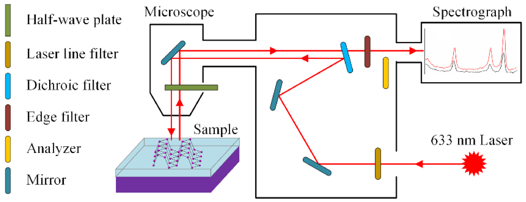
2.2. Experiments
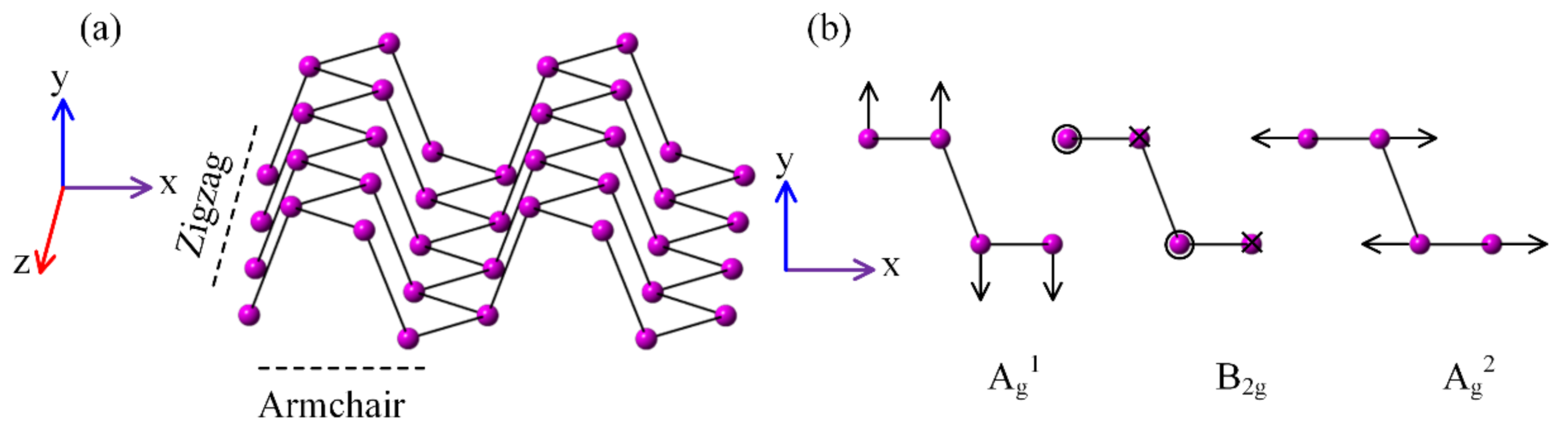
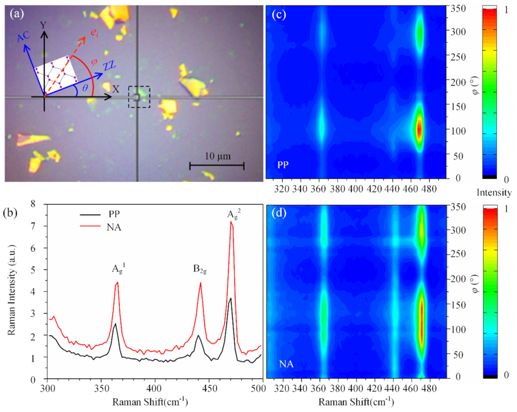
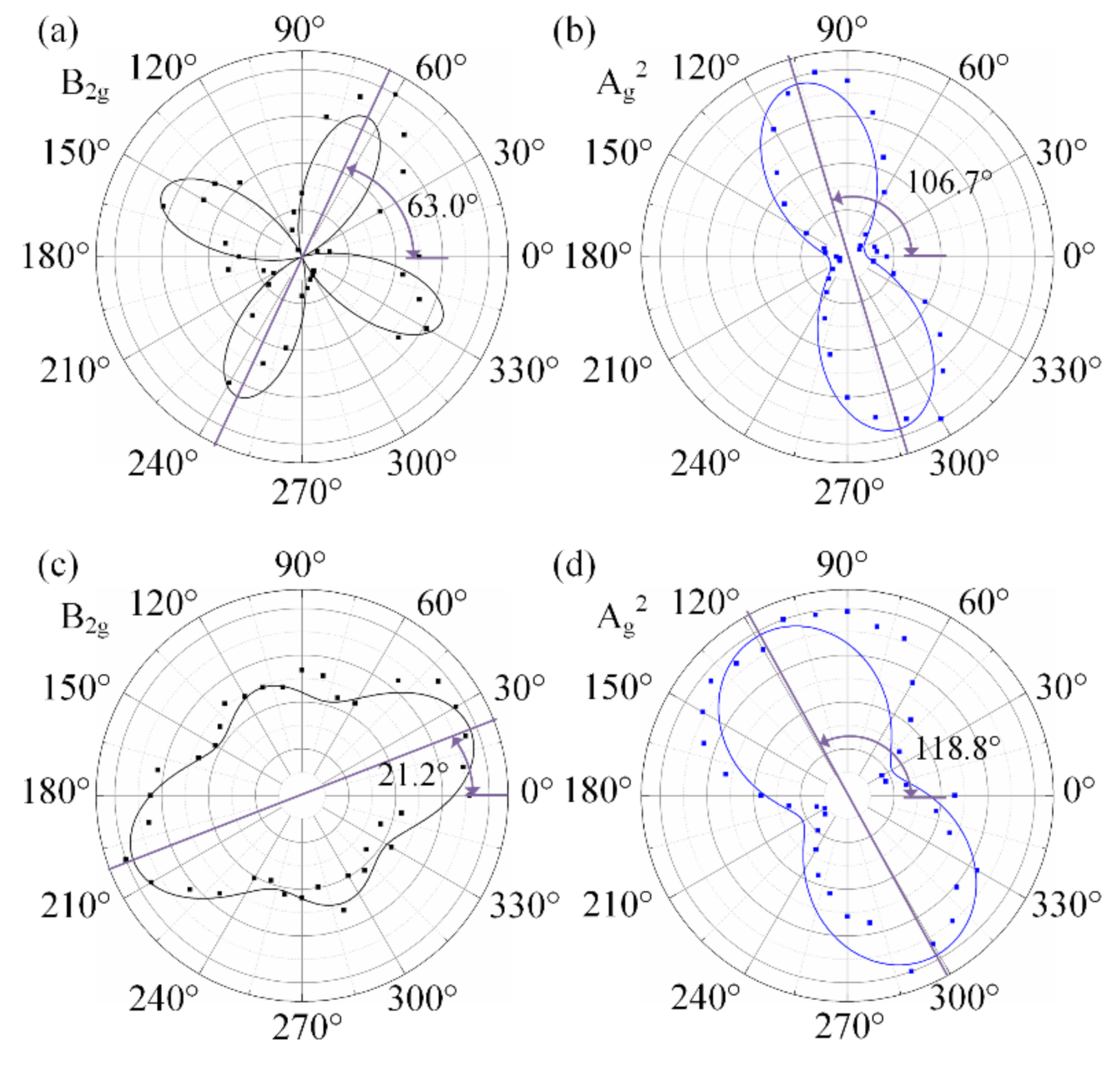
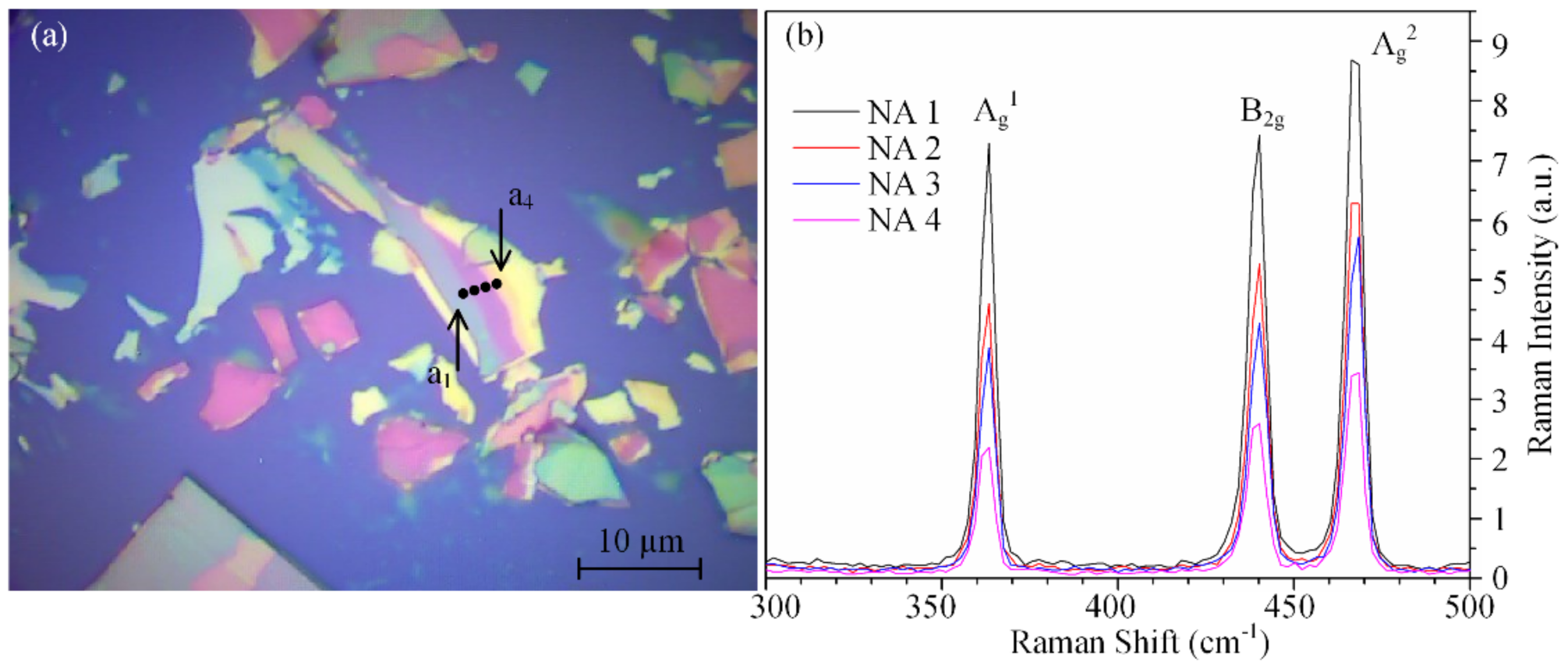
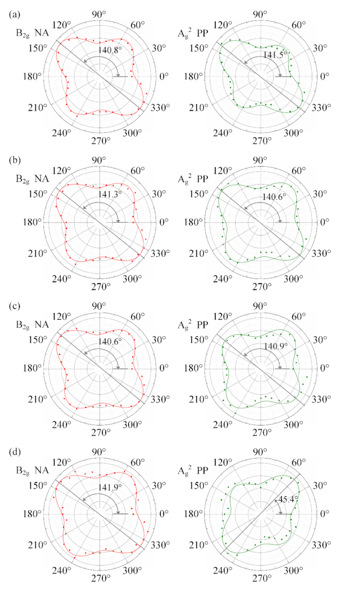
3. Results and Discussions
4. Conclusions
Author Contributions
Funding
Acknowledgments
Conflicts of Interest
References
- Li, L.; Yu, Y.; Ye, G.J.; Ge, Q.; Ou, X.; Wu, H.; Feng, D.; Chen, X.H.; Zhang, Y. Black phosphorus field-effect transistors. Nat. Nanotechnol. 2014, 9, 372–377. [Google Scholar] [CrossRef] [PubMed] [Green Version]
- Wang, Q.H.; Kalantar-Zadeh, K.; Kis, A.; Coleman, J.N.; Strano, M.S. Electronics and optoelectronics of two-dimensional transition metal dichalcogenides. Nat. Nanotechnol. 2012, 7, 699–712. [Google Scholar] [CrossRef] [PubMed]
- Geim, A.K.; Novoselov, K.S. The rise of graphene. Nat. Mater. 2007, 6, 183–191. [Google Scholar] [CrossRef] [PubMed]
- Drissi, L.B.; Sadki, S.; Sadki, K. Phosphorene under strain: Electronic, mechanical and piezoelectric responses. J. Phys. Chem. Solids 2018, 112, 137–142. [Google Scholar] [CrossRef]
- Ling, X.; Huang, S.; Hasdeo, E.H.; Liang, L.; Parkin, W.M.; Tatsumi, Y.; Nugraha, A.R.; Puretzky, A.A.; Das, P.M.; Sumpter, B.G.; et al. Anisotropic electron-photon and electron-phonon interactions in black phosphorus. Nano Lett. 2016, 16, 2260–2267. [Google Scholar] [CrossRef] [PubMed]
- Fei, R.; Faghaninia, A.; Soklaski, R.; Yan, J.A.; Lo, C.; Yang, L. Enhanced thermoelectric efficiency via orthogonal electrical and thermal conductances in phosphorene. Nano Lett. 2014, 14, 6393–6399. [Google Scholar] [CrossRef] [Green Version]
- Fei, R.; Yang, L. Strain-engineering the anisotropic electrical conductance of few-layer black phosphorus. Nano Lett. 2014, 14, 2884–2889. [Google Scholar] [CrossRef] [Green Version]
- Xia, F.; Wang, H.; Jia, Y. Rediscovering black phosphorus as an anisotropic layered material for optoelectronics and electronics. Nat. Commun. 2014, 5, 4458. [Google Scholar] [CrossRef] [Green Version]
- Li, Y.; Hu, Z.; Lin, S.; Lai, S.K.; Ji, W.; Lau, S.P. Giant anisotropic raman response of encapsulated ultrathin black phosphorus by uniaxial strain. Adv. Funct. Mater. 2017, 27, 1600986. [Google Scholar] [CrossRef]
- Wang, Y.; Cong, C.; Fei, R.; Yang, W.; Chen, Y.; Cao, B.; Yang, L.; Yu, T. Remarkable anisotropic phonon response in uniaxially strained few-layer black phosphorus. Nano Res. 2015, 8, 3944–3953. [Google Scholar] [CrossRef]
- Rodin, A.S.; Carvalho, A.; Castro Neto, A.H. Strain-induced gap modification in black phosphorus. Phys. Rev. Lett. 2014, 112, 176801. [Google Scholar] [CrossRef] [PubMed] [Green Version]
- Tran, V.; Soklaski, R.; Liang, Y.; Yang, L. Layer-controlled band gap and anisotropic excitons in few-layer black phosphorus. Phys. Rev. B 2014, 89, 235319. [Google Scholar] [CrossRef] [Green Version]
- Na, J.; Lee, Y.T.; Lim, J.A.; Hwang, D.K.; Kim, G.-T.; Choi, W.K.; Song, Y.-W. Few-layer black phosphorus field-effect transistors with reduced current fluctuation. ACS Nano 2014, 8, 11753–11762. [Google Scholar] [CrossRef] [PubMed]
- Liu, H.; Neal, A.T.; Zhu, Z.; Luo, Z.; Xu, X.; Tomanek, D.; Ye, P.D. Phosphorene: An unexplored 2D semiconductor with a high hole mobility. ACS Nano 2014, 8, 4033–4041. [Google Scholar] [CrossRef] [Green Version]
- Du, Y.; Maassen, J.; Wu, W.; Luo, Z.; Xu, X.; Ye, P.D. Auxetic black phosphorus: A 2D material with negative poisson’s ratio. Nano Lett. 2016, 16, 6701–6708. [Google Scholar] [CrossRef] [Green Version]
- Jiang, J.-W.; Park, H.S. Negative poisson’s ratio in single-layer black phosphorus. Nat. Commun. 2014, 5, 4727. [Google Scholar] [CrossRef] [Green Version]
- Qiao, J.; Kong, X.; Hu, Z.-X.; Yang, F.; Ji, W. High-mobility transport anisotropy and linear dichroism in few-layer black phosphorus. Nat. Commun. 2014, 5, 4475. [Google Scholar] [CrossRef] [Green Version]
- Zhang, G.; Huang, S.; Chaves, A.; Song, C.; Özçelik, V.O.; Low, T.; Yan, H. Infrared fingerprints of few-layer black phosphorus. Nat. Commun. 2017, 8, 14071. [Google Scholar] [CrossRef]
- Mak, K.F.; Lee, C.; Hone, J.; Shan, J.; Heinz, T.F. Atomically thin MoS2: A new direct-gap semiconductor. Phys. Rev. Lett. 2010, 105, 136805. [Google Scholar] [CrossRef] [Green Version]
- Ling, X.; Wang, H.; Huang, S.; Xia, F.; Dresselhaus, M.S. The renaissance of black phosphorus. Proc. Natl. Acad. Sci. USA 2015, 112, 4523–4530. [Google Scholar] [CrossRef] [Green Version]
- Wu, J.; Mao, N.; Xie, L.; Xu, H.; Zhang, J. Identifying the crystalline orientation of black phosphorus using angle-resolved polarized Raman spectroscopy. Angew. Chem. Int. Ed. 2015, 54, 2366–2369. [Google Scholar] [CrossRef] [PubMed]
- Li, L.; Kim, J.; Jin, C.; Ye, G.J.; Qiu, D.Y.; da Jornada, F.H.; Shi, Z.; Chen, L.; Zhang, Z.; Yang, F.; et al. Direct observation of the layer-dependent electronic structure in phosphorene. Nat. Nanotechnol. 2017, 12, 21–25. [Google Scholar] [CrossRef] [PubMed] [Green Version]
- Zhang, R.; Wu, S.; Liu, L.; Fu, X.; Gao, S.; Hu, X. Adaptive-angle scanning method for 3D measurement with atomic force microscopy. Meas. Sci. Technol. 2019, 30, 095005. [Google Scholar] [CrossRef]
- Cao, K.; Li, P.; Zhang, Y.; Chen, T.; Wang, X.; Zhang, S.; Liu, J.; Wang, H. In situ tem investigation on ultrafast reversible lithiation and delithiation cycling of Sn@C yolk-shell nanoparticles as anodes for lithium ion batteries. Nano Energy 2017, 40, 187–194. [Google Scholar] [CrossRef]
- Wang, H.; Li, K.; Cheng, Y.; Wang, Q.; Yao, Y.; Schwingenschlogl, U.; Zhang, X.; Yang, W. Interaction between single gold atom and the graphene edge: A study via aberration-corrected transmission electron microscopy. Nanoscale 2012, 4, 2920–2925. [Google Scholar] [CrossRef]
- Ribeiro, H.B.; Pimenta, M.A.; de Matos, C.J.S. Raman spectroscopy in black phosphorus. J. Raman Spectrosc. 2018, 49, 76–90. [Google Scholar] [CrossRef]
- Malka, D.; Adler Berke, B.; Tischler, Y.; Zalevsky, Z. Improving Raman spectra of pure silicon using super-resolved method. J. Optics-UK 2019, 21, 075801. [Google Scholar] [CrossRef]
- Malka, D.; Berkovic, G.; Tischler, Y.; Zalevsky, Z. Super-resolved Raman spectra of toluene and toluene–chlorobenzene mixture. Spectrosc. Lett. 2015, 48, 431–435. [Google Scholar] [CrossRef]
- Cen, H.; Kang, Y.; Lei, Z.; Qin, Q.; Qiu, W. Micromechanics analysis of Kevlar-29 aramid fiber and epoxy resin microdroplet composite by Micro-Raman spectroscopy. Compos. Struct. 2006, 75, 532–538. [Google Scholar] [CrossRef]
- Kang, Y.; Qiu, Y.; Lei, Z.; Hu, M. An application of Raman spectroscopy on the measurement of residual stress in porous silicon. Opt. Laser. Eng. 2005, 43, 847–855. [Google Scholar] [CrossRef]
- Qiu, W.; Li, Q.; Lei, Z.; Qin, Q.; Deng, W.; Kang, Y. The use of a carbon nanotube sensor for measuring strain by micro-Raman spectroscopy. Carbon 2013, 53, 161–168. [Google Scholar] [CrossRef]
- Kim, J.; Lee, J.U.; Lee, J.; Park, H.J.; Lee, Z.; Lee, C.; Cheong, H. Anomalous polarization dependence of Raman scattering and crystallographic orientation of black phosphorus. Nanoscale 2015, 7, 18708–18715. [Google Scholar] [CrossRef] [PubMed] [Green Version]
- Mao, N.; Wu, J.; Han, B.; Lin, J.; Tong, L.; Zhang, J. Birefringence-directed raman selection rules in 2D black phosphorus crystals. Small 2016, 12, 2627–2633. [Google Scholar] [CrossRef] [PubMed]
- Zhang, S.; Mao, N.; Wu, J.; Tong, L.; Zhang, J.; Liu, Z. In-plane uniaxial strain in black phosphorus enables the identification of crystalline orientation. Small 2017, 13, 1700466. [Google Scholar] [CrossRef] [PubMed]
- Ribeiro, H.B.; Pimenta, M.A.; de Matos, C.J.S.; Moreira, R.L.; Rodin, A.S.; Zapata, J.D.; de Souza, E.A.T.; Castro Neto, A.H. Unusual angular dependence of the Raman response in black phosphorus. ACS Nano 2015, 9, 4270–4276. [Google Scholar] [CrossRef] [PubMed]
- Lu, W.; Nan, H.; Hong, J.; Chen, Y.; Zhu, C.; Liang, Z.; Ma, X.; Ni, Z.; Jin, C.; Zhang, Z. Plasma-assisted fabrication of monolayer phosphorene and its Raman characterization. Nano Res. 2014, 7, 853–859. [Google Scholar] [CrossRef] [Green Version]
- Favron, A.; Gaufres, E.; Fossard, F.; Phaneuf-L’Heureux, A.L.; Tang, N.Y.; Levesque, P.L.; Loiseau, A.; Leonelli, R.; Francoeur, S.; Martel, R. Photooxidation and quantum confinement effects in exfoliated black phosphorus. Nat. Mater. 2015, 14, 826–832. [Google Scholar] [CrossRef]
- Wang, X.; Jones, A.M.; Seyler, K.L.; Tran, V.; Jia, Y.; Zhao, H.; Wang, H.; Yang, L.; Xu, X.; Xia, F. Highly anisotropic and robust excitons in monolayer black phosphorus. Nat. Nanotechnol. 2015, 10, 517–521. [Google Scholar] [CrossRef] [Green Version]
- Chen, H.; Fei, W.; Zhou, J.; Miao, C.; Guo, W. Layer identification of colorful black phosphorus. Small 2017, 13, 1602336. [Google Scholar] [CrossRef]
- Li, D.; Jussila, H.; Karvonen, L.; Ye, G.; Lipsanen, H.; Chen, X.; Sun, Z. Polarization and thickness dependent absorption properties of black phosphorus: New saturable absorber for ultrafast pulse generation. Sci. Rep. 2015, 5, 15899. [Google Scholar] [CrossRef] [Green Version]
- Low, T.; Rodin, A.S.; Carvalho, A.; Jiang, Y.; Wang, H.; Xia, F.; Castro Neto, A.H. Tunable optical properties of multilayer black phosphorus thin films. Phys. Rev. B 2014, 90, 075434. [Google Scholar] [CrossRef] [Green Version]
- Song, Q.; Pan, X.; Wang, H.; Zhang, K.; Tan, Q.; Li, P.; Wan, Y.; Wang, Y.; Xu, X.; Lin, M.; et al. The in-plane anisotropy of WTe2 investigated by angle-dependent and polarized raman spectroscopy. Sci. Rep. 2016, 6, 29254. [Google Scholar] [CrossRef] [PubMed] [Green Version]
- Wolverson, D.; Crampin, S.; Kazemi, A.S.; Ilie, A.; Bending, S.J. Raman spectra of monolayer, few-layer, and bulk ReSe2: An anisotropic layered semiconductor. ACS Nano 2014, 8, 11154–11164. [Google Scholar] [CrossRef] [PubMed] [Green Version]
- Lin, H.C.; Feng, Z.C.; Chen, M.S.; Shen, Z.X.; Ferguson, I.T.; Lu, W. Raman scattering study on anisotropic property of wurtzite GaN. J. Appl. Phys. 2009, 105, 036102. [Google Scholar] [CrossRef]
- Saito, R.; Tatsumi, Y.; Huang, S.; Ling, X.; Dresselhaus, M.S. Raman spectroscopy of transition metal dichalcogenides. J. Phys. Condens. Mat. 2016, 28, 353002. [Google Scholar] [CrossRef]
- Zheng, W.; Zheng, R.S.; Wu, H.L.; Li, F.D. Strongly anisotropic behavior of A1(TO) phonon mode in bulk AlN. J. Alloys Compd. 2014, 584, 374–376. [Google Scholar] [CrossRef]
- Bao, H.; Li, R.; Xing, H.; Qu, C.; Li, Q.; Qiu, W. Crystalline orientation identification of phosphorene using polarized raman spectroscopy without analyzer. Appl. Sci. Basel 2019, 9, 2198. [Google Scholar] [CrossRef] [Green Version]


| Ag | B1g | B2g | B3g |
|---|---|---|---|
| Sampling Spot | a1 | a2 | a3 | a4 | |
|---|---|---|---|---|---|
| B2g | NA | 140.8° | 141.3° | 140.6° | 141.9° |
| Ag2 | PP | 141.5° − 90° = 51.5° | 140.6° − 90° = 50.6° | 140.9° − 90° = 50.9° | 45.4° + 90° = 135.4° |
Publisher’s Note: MDPI stays neutral with regard to jurisdictional claims in published maps and institutional affiliations. |
© 2020 by the authors. Licensee MDPI, Basel, Switzerland. This article is an open access article distributed under the terms and conditions of the Creative Commons Attribution (CC BY) license (http://creativecommons.org/licenses/by/4.0/).
Share and Cite
Li, R.; Shang, Y.; Xing, H.; Wang, X.; Sun, M.; Qiu, W. Orientation Identification of the Black Phosphorus with Different Thickness Based on B2g Mode Using a Micro-Raman Spectroscope under a Nonanalyzer Configuration. Materials 2020, 13, 5572. https://doi.org/10.3390/ma13235572
Li R, Shang Y, Xing H, Wang X, Sun M, Qiu W. Orientation Identification of the Black Phosphorus with Different Thickness Based on B2g Mode Using a Micro-Raman Spectroscope under a Nonanalyzer Configuration. Materials. 2020; 13(23):5572. https://doi.org/10.3390/ma13235572
Chicago/Turabian StyleLi, Rubing, Yongchao Shang, Huadan Xing, Xiaojie Wang, Mingyuan Sun, and Wei Qiu. 2020. "Orientation Identification of the Black Phosphorus with Different Thickness Based on B2g Mode Using a Micro-Raman Spectroscope under a Nonanalyzer Configuration" Materials 13, no. 23: 5572. https://doi.org/10.3390/ma13235572