1. Introduction
Zinc oxide exhibits high thermal and chemical stability and has been studied for decades [
1,
2]. ZnO is a semiconductor with a direct band-gap of
3.3 eV [
3,
4] similar to the value reported to gallium nitride (
3.4 eV) [
5], however the binding energy of zinc oxide exciton (60 meV) [
4] is 2.4 times larger than that of GaN (25 meV) [
5]. These features indicate that ZnO is a promising material for short-wavelength optoelectronic devices such as light-emitting and laser diodes [
6]. Due to good optical transmittance in the visible spectral range zinc oxide is used as a transparent electrode in organic and hybrid solar cells [
7,
8]. Moreover, ZnO is used in thin-film transistors [
9] and gas sensors [
10]. Zinc oxide is a very good candidate for space applications due to its stability to high energy radiation [
1]. On the other hand, ZnO can be easily etched in acids and alkali [
11]. This feature is commonly used to produce ZnO in form of nanosheeds, nanoshells, multipods, nanorods or nanowires typicaly implemented as periodic structures using a number of methods [
2,
12].
The structural and optical properties of ZnO films strongly depend on the fabrication conditions that affect the optimal performance of the device. It has been shown that optical constants (complex refractive index or complex dielectric function) of zinc oxide demonstrate significant film-thickness relationship, especially for thicknesses below 20 nm [
3,
13,
14,
15]. Moreover, Pal et al. [
3] revealed the influence of the substrate on the optical properties of ZnO films. Therefore, systematic study of the properties of zinc oxide layers fabricated under various growing conditions is desirable. This analysis was performed for ZnO produced by different techniques such as atomic layer deposition [
3,
4,
9], electron beam evaporation [
16,
17,
18,
19], magnetron sputtering [
10,
19,
20], chemical vapour deposition [
6], spin coating [
21,
22] as well as molecular beam epitaxy [
23]. In addition, the existence of oxygen or zinc vacancies and their concentration in ZnO, significantly affects luminescence and photocatalytic properties [
22], depending on the method of production.
Electron beam physical vapour deposition (e-beam PVD) technique is commonly used to produce both metallic [
24,
25,
26] and oxide coatings [
27] including zinc oxide films [
16,
19]. The influence of microstructure on the optical response of zinc oxide films fabricated under various conditions, such as the substrate temperature (and/or annealing after deposition) as well as deposition rate, has been investigated in recent years [
16,
18,
19]. It has been reported that increasing the substrate temperature and/or annealing of ZnO after deposition significantly improves their stoichiometry, resistivity, free carrier mobility and optical transparency [
16,
18]. The post-evaporation annealing process in oxygen atmosphere also serves to ensure that there is no deficiency of oxygen atoms in the deposited films [
19], due to decomposition and release oxygen into the vacuum [
28,
29,
30,
31]. This process was also observed for ZnO films [
19,
20].
In this paper we show the influence of substrate temperature during deposition by means of the e-beam technique and annealing in ultra high vacuum (UHV) conditions on the microstructure and optical properties of zinc oxide films. The above relationship was studied based on the results of atomic force microscopy (AFM), scanning electron microscopy (SEM), X-ray diffraction (XRD), X-ray photoelectron spectroscopy (XPS) and spectroscopic ellipsometry (SE) measurements. The above-mentioned methods were used to explain the influence of ZnO decomposition and segregation of Zn atoms on the optical response of the deposited films.
2. Materials and Methods
Fabrication of the samples has been conducted using the PVD75 e-beam evaporation system from Lesker (St. Leonards-on-Sea, UK). ZnO films have been deposited from 4 N ZnO pieces in graphite crucible onto polished Si substrates (100). Silicon is widely used in fabrication of a variety of optical devices (e.g., [
32,
33]). Substrates were located 40 cm away from the crucible. Three sets of samples have been fabricated—with the substrate at room temperature (RT), at 100 and 200
C. The base pressure was
Torr, however, due to the decomposition of ZnO, during the deposition process the pressure approached
Torr. The deposition rate and total film thickness were monitored by two quartz weights inside the deposition chamber. The nominal deposition rate was 0.3 Å/s, however, due to the decomposition of ZnO, it is difficult to estimate the true value (although it is expected to be within 30% of the nominal value). After the deposition, the samples were annealed for two hours at 300, 500 and 800
C. The annealing was performed in a UHV preparation chamber (base pressure
mbar). The list of prepared samples is summarized in
Table 1.
After cooling to room temperature, the samples were transferred without venting to the analysis chamber (base pressure mbar) for XPS measurements. The incident radiation was produced by Al K source (1486.6 eV) at 55 degrees with respect to the normal of the sample. The energy of photoelectrons was analyzed by the VG-Scienta R3000 (Uppsala, Sweden) spectrometer (the energy step was set at = 0.1 eV. For quantitative analysis, the experimental data was fitted to Gauss–Lorentz shapes by using CasaXPS software (version 2.3.16, Casa Software Ltd., Teignmouth, UK).
The surface topography of the films was examined by means of the AFM Innova device from Bruker (Billerica, MA, USA) equipped with the standard Si tips for a tapping mode. Roughness parameters
(the arithmetical mean deviation):
and
(the root mean squared roughness):
where
and
N are the current surface height value and the number of points measured, respectively. They were calculated based on the images, recorded for an area 2
m × 2
m, using the NanoScope Analysis software (version 1.40). Scanning electron microscopy (SEM) investigations were performed with a Quanta 3D FEG (FEI, Hillsboro, OR, USA) (EHT = 30 kV) device.
The Phillips X’Pert (Malvern Panalytical Ltd., Malvern, UK) device with Cu K radiation ( = 1.5418 Å) and X’Celerator Scientific (Malvern Panalytical Ltd., Malvern, UK) detector was used to record the XRD patters of the investigated samples. These measurements were performed in the range from 2 = 20 to 60 .
The thickness and optical constants of the prepared thin films were investigated by means of the V-VASE device from J.A. Woollam Co., Inc., Lincoln, NE, USA. The ellipsometric azimuths and were measured for three angles of incidence (65, 70 and 75) in the NIR-vis-UV spectral range (193–2000 nm; 0.6–6.5 eV). The analysis of ellipsometric data was performed using the WVASE32 software (J.A. Woollam Co., Inc.).
3. Results
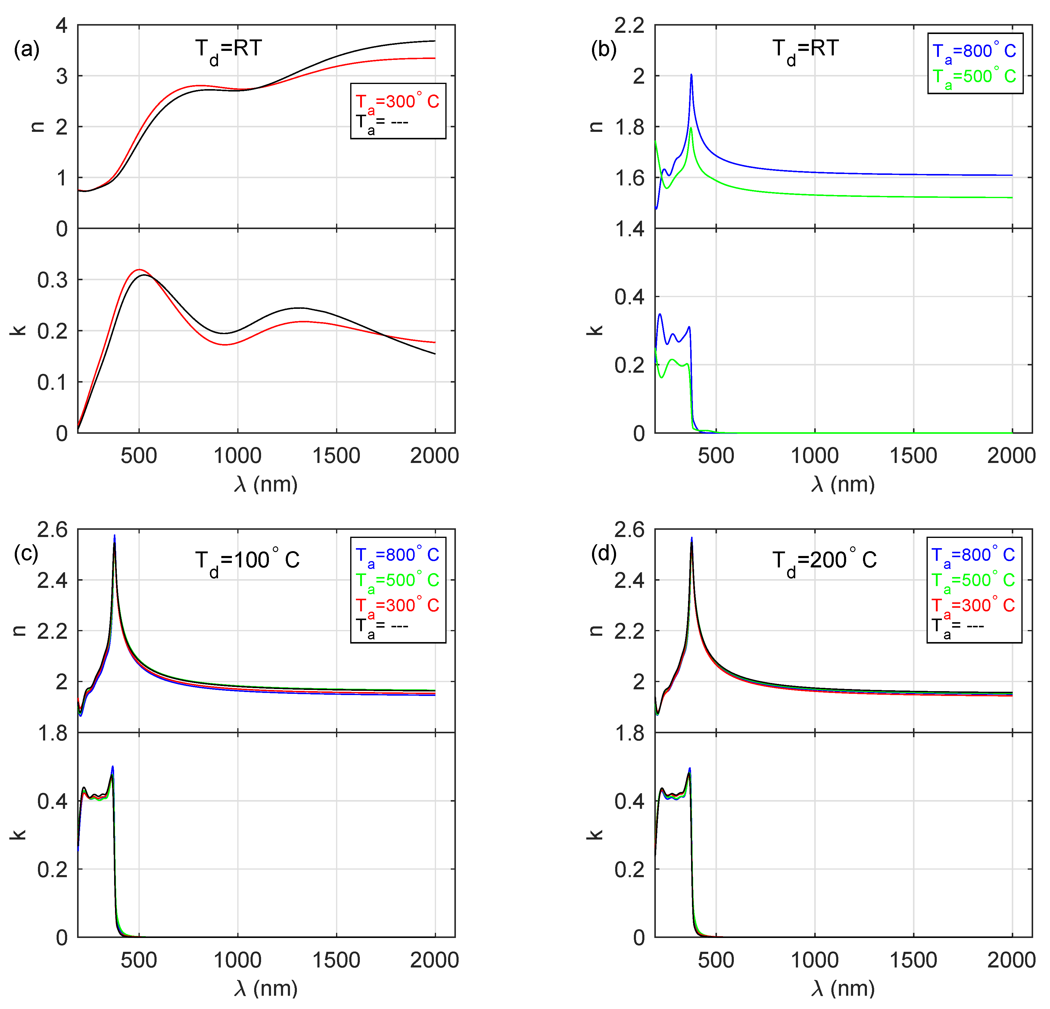
Spectroscopic ellipsometry (SE) was used to obtain the thickness of the zinc oxide film as well as the optical constants of the deposited coatings. The measured
and
ellipsometric azimuths for S_ RT, S_ RT_ 800C and S_ 200C_ 800C are presented in
Figure 1. The
and
curves vary significantly for films fabricated in different conditions. Spectra shown in
Figure 1a exhibit metallic-like behaviour, while data presented in
Figure 1b,c are typical for a semiconducting material. Oscillations in the ellipsometric
and
angles for wavelengths longer than about 390 nm for the S_ RT_ 800C sample (
Figure 1b) indicate that the thickness of the layer is significantly greater compared to the thickness of S_ 200C_ 800C film. The thickness of the layer and its optical constants were determined by means of the five-medium optical model of a sample (from bottom to top: substrate-Si∖native SiO
∖ZnO film∖rough layer∖ambient). The complex refractive index of the ZnO film (
, where
n and
k are the real part of
and the extinction coefficient, respectively) was parametrised using a model containing the following components/oscillators:
a Sellemeier-type dispersion relation (a Pole oscillator; ),
a Drude term (; for the S_RT and S_ RT_ 300 samples) or a Tauc–Lorentz oscillator (; for the other specimens) and
a sum of Gaussian oscillators ().
The selection of these oscillators was performed based on the shape of the measured ellipsometric azimuths (see
Figure 1). The complex refractive index of the deposited film can be written in the following form:
or
In Equations (
3) and (
4),
is the high-frequency dielectric constant,
and
are the pole oscillator position and magnitude, respectively, while
is the unscreened plasma energy and
is the free-carrier dumping. The quantities
A,
E and
(with adequate subscripts) represent amplitude, energy and broadening of the line shape, respectively, while
is the band gap energy. Mathematical formulas for the particular line shapes can be found elsewhere [
34,
35]. The form of
(Equation (
3) or Equation (
4)) used to determine optical constants of the produced films are summarized in
Table 2.
The complex refractive index of Si and SiO
were employed from the database of optical constants [
35]. The thickness of native oxide was set to be 2.3 nm and was established in the separate experiment [
36]. The imperfect surface of the deposited film (the rough layer) was described based on the Bruggeman Effective Medium Approximation (EMA) model [
34,
35]. In this approach, the optical constants of the rough film are represented as a combination of optical properties of ZnO film and ambient (the assumed volume fraction of each medium was set to be 1/2). The model quantities were minimized to reduce the standard mean squared error (
) [
35]:
In Equation (
5)
N and
P are the total number of data points and the number of fitted model parameters respectively. The
and
represent measured (with the superscript ‘exp’) or calculated (with the superscript ‘mod’) ellipsometric azimuths. Quantities
and
are standard deviations for measured
and
angles. Example of the fits are presented in
Figure 1. It should be noted that the reduced mean squared error (
) was below 2.57 for all the samples produced, which means that the calculated
and
values are in a very good agreement with the experimental data.
The thicknesses of the prepared films (
) are in the range from about 37 to 325 nm, while thicknesses of the rough layer (
) were found to be 5–41 nm (see
Table 2), whereas for the samples deposited at room temperature these values are one order of magnitude higher, than those obtained for the specimens produced at higher temperatures. The real part (
n) of the complex refractive index (
) and the extinction coefficient (
k) determined by the spectroscopic ellipsometry method are presented in
Figure 2. The spectra shown in
Figure 2a (for S_ RT and S_ RT_ 300C samples) exhibit metallic-like behaviour (noticeable extinction coefficient in the UV-vis-IR), however without the strong Drude contribution characteristic for conductors. Plasma energy (
), found during the analysis of the SE data, established to be 1.7 and 1.8 eV for S_ RT_ 300C and S_ RT samples, respectively, is much lower than that reported for pure zinc (10 eV) [
37]. The
n and
k spectra presented in
Figure 2b–d are typical for semiconducting materials, i.e., a normal dispersion for longer wavelengths and interband transitions in the high-energy region.
The band-gap energy (
) for the produced ZnO films was determined during the parametrisation of their optical constants (a Tauc–Lorentz oscillator; see Equation (
3)) and are summarized in
Table 3. Values of
were established to be 3.2 eV for the layers deposited at 100 and 200
C as well as at RT (however only for films annealed at 500 and 800
C) and are in a perfect agreement with published data [
3,
4,
13,
15,
38]. For metallic-like samples (S_RT and S_RT_300C) the band-gap energy could not be determined.
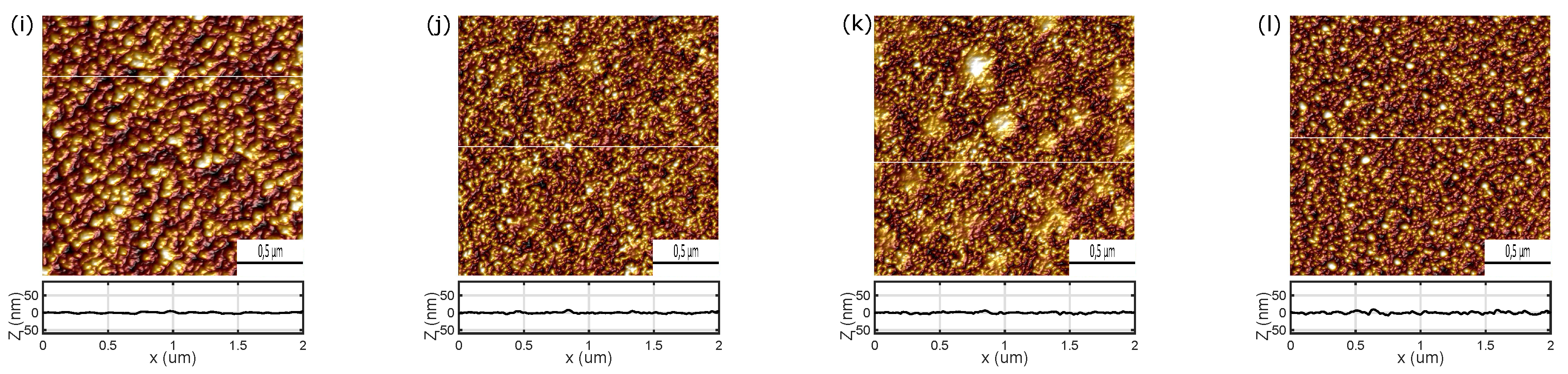
AFM images of the ZnO films deposited at RT, at 100
C and at 200
C (both non-annealed and annealed after deposition) are presented in
Figure 3. Surfaces of all samples exhibit the nanogranular structure with the lateral size of grains smaller than 100 nm (for specimens produced at RT;
Figure 3a) or 50 nm (for the other surfaces;
Figure 3b,c). It should be taken into account that the samples deposited at RT exhibit significantly expanded surface compared to the surface of the other ZnO layers (see profiles in
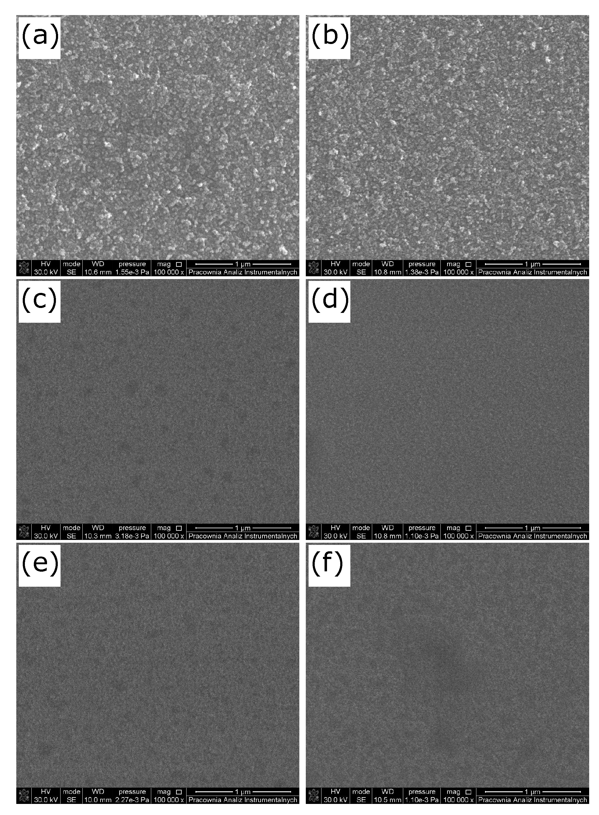
Figure 3). The surface morphology of the deposited films has been confirmed in the SEM measurements (see
Figure A1 in
Appendix A). For ZnO films deposited at RT the average roughness (
) is about 20 nm (see
Table 2) and the maximum roughness (
) 150–160 nm, whereas for the zinc oxide layers grown at higher temperatures (100 and 200
C) these values are significantly lower (
= 1.5–2.9 nm;
= 11–32 nm).
The XRD patterns recorded for the deposited coatings are presented in
Figure 4. Diffraction peaks related to ZnO are observed at 2
32
(100), 34
(002), 36
(101), 48
(102) and 57
(110), while the signal recorded at 2
39
(100), 43
(101) and 55
(102) can be referred to metallic zinc. The strong and narrow peak at 2
33
can be assigned to the substrate-Si (200). The average crystallite size (
) determined for the identified Zn and ZnO phases, summarized in
Table 4, has been estimated based on the Scherrer formula:
where
is the X-ray wavelength and
is the full-width at half-maximum (FWHM) of the Bragg diffraction peak at angle 2
.
The layer deposited at RT (a sample S_ RT; see
Figure 4a) consists of both ZnO and Zn crystallites, which are relatively small (
= 6–13 nm) and show a number of orientations. Annealing of the deposited film at 300
C (a sample S_ RT_ 300C) does not change the phase composition of the coating. The layers annealed at higher temperatures (
500
C; samples S_ RT_ 500C and S_ RT_ 800C) contain only ZnO grains. The most prominent XRD peaks (2
= 30
–40
) for these two samples are narrower than that recorded for S_ RT and S_ RT_ 300C—the average crystallite size is in the range 11–15 nm and 12–25 nm for S_ RT_ 500C and S_ RT_ 800C films, respectively. It should be noted that no growth direction is privileged. Completely different XRD patterns have been registered for samples deposited at 100 and 200
C (see
Figure 4b,c). Those films are composed of only ZnO (200) crystallites (the other XRD peaks show negligible intensity). The registered (200) direction of growth (as provileged orientation) was observed earlier for ZnO layers produced using various methods [
14,
17,
19]. The average crystallite size increases with the increase in the annealing temperature from about 19 to about 30 nm (see
Figure 4d).
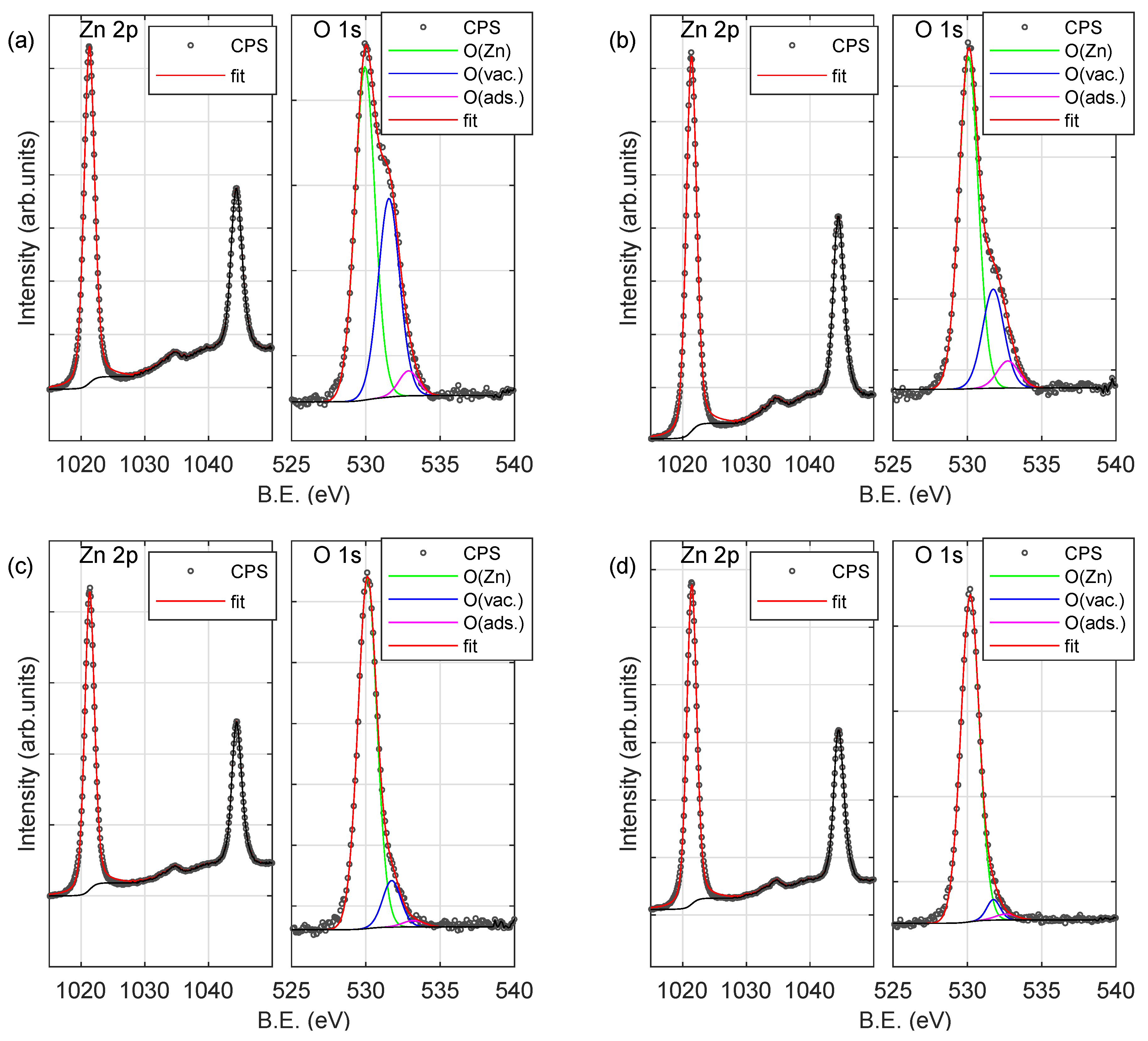
To investigate the chemical state of the surface of the produced samples the Zn 2p, O 1s and C 1s peaks have been recorded.
Figure 5 shows Zn 2p and O 1s XPS signals for samples deposited at room temperature (both non-annealed and annealed at 300, 500 and 800
C). The spectrum of zinc exhibits a characteristic doublet at 1022 eV (2p 3/2) and 1045 eV (2p 1/2) [
14,
20,
39]. The O 1s signal consists of three components. The most prominent (with maximum at 530 eV; O(Zn)) can be assigned to oxygen atoms in the ZnO compound [
14,
20,
21,
40,
41]. The second one (at 531 eV; O(vac.)) is associated with the O
in the oxygen-deficient region (vacancies) within the matrix of zinc oxide [
42,
43]. The last one (at 532 eV; O(ads.))—is connected to the adsorbed oxygen at the surface of the specimen [
41]. It should be noted that the intensity (and thus concentration) of the second and the third components of the O 1s peak significantly decreases with the increase of the annealing temperature. Concentrations of particular elements are summarized in
Table 5. The concentration of Zn (C
) and O bounded with Zn (C
) atoms increases with the increase in the annealing temperature (for all series of samples). The opposite can be observed for the adsorbed oxygen (C
) and oxygen ions (O
) in the oxygen-deficient region as well as carbon (related to both sp
hybridization and adsorbed at the surface as CO
) [
39]. Despite the fact that the concentration of carbon (C
) for the non-annealed sample is 12–15% (see
Table 5), it decreases rapidly with increasing annealing temperature and is about 1% for samples annealed at 800
C.
Deconvolution of the O 1s signal allowed us to determine the ratio of Zn and O atoms at the surface of the prepared films taking into account total concentration of oxygen (C
) or the part related only to O (C
) atoms bounded with Zn atoms. These estimated ratios are presented in
Table 6. The ratio between zinc and oxygen atoms (total) for the non-annealed samples (S_ RT, S_ 100C and S_ 200C) is about 1 and increases to about 1.6 with the increase of the annealing temperature. Significantly higher values have been determined taking into account only the part of O 1s peak related to oxygen atoms bounded with zinc atoms. These values are in the range from about 1.5 to 1.9 (see
Table 6).
4. Discussion
Both AFM (see
Figure 3 and
Table 2) and XRD (see
Figure 4 and
Table 4) results show that the grain size perpendicular to the surface increases with annealing temperature as the grains coalesce, regardless of the sample deposition temperature. The trend is similar for the lateral grain size, however in the case of ZnO deposited at RT the lateral grain size is already so large that no annealing-induced coalescence is expected.
Further results presented in the previous section unambiguously show that the main changes during annealing were observed for the samples deposited at room temperature. The changes were much less prominent for samples deposited at elevated temperatures. Therefore in this section, we focus our attention on the explanation of this phenomenon and on the effect of annealing on microstructure and optical properties of the fabricated films.
First, it was noticed that the thicknesses of ZnO films deposited onto substrates at elevated temperatures during the deposition process (100 and 200
C) as determined form ellipsometric measurements are significantly lower (by an order of magnitude) than in the case of films deposited onto substrates at room temperature (see
Table 2). Second, as described in the Results section, the permittivity of these films exhibits a more oxide-like behaviour (
Figure 2b–d), whereas films deposited onto substrates at room temperature have more metal-like characteristics (
Figure 2a). This might be a consequence of two phenomena—ZnO decomposition during the deposition process (which will result in an excess of Zn atoms in the deposited film) as well as subsequent excess Zn atom surface segregation as desorption in elevated temperatures, which would improve stoichiometry. The details are described below.
During the e-beam evaporation process, many oxide materials are known to decompose [
28,
29,
30,
31] releasing oxygen into the vacuum. The decomposition of ZnO has also been observed [
19,
20]. Thus, to ensure there is no deficiency of oxygen atoms in the evaporated film, it has been proposed to perform the deposition process in an oxygen atmosphere [
19]. In our case, the ZnO films have been deposited in a high vacuum. This approach results in the evaporated films containing an excess of Zn atoms with respect to typical ZnO stoichiometry. Since samples fabricated using e-beam technology are typically polycrystalline, the excess Zn atoms are expected to segregate to the ZnO grain boundaries as well as to the film’s free surface, as this process would result in the release of the elastic strain energy accumulated in the non-stoichiometric ZnO crystallites [
44,
45]. This is due to the fact that within the crystallites there is a limited number of lattice vacancies which enable the excess Zn atoms to occupy substitutional lattice sites. Most of the excess Zn atoms are therefore expected to occupy the interstitial lattice sites. This would induce much higher local distortions (strain) to the crystal lattice. Because of numerous lattice vacancies being present on the free surface and at the grain boundaries, there are more substitutional lattice sites in those regions for the excess Zn atoms to occupy. Moreover, the excess Zn atoms present in the interstitial sites on the surface and at the grain boundaries induce strain in a lower volume of the crystal lattice than the excess Zn atoms present in the interstitial lattice sites inside the ZnO grains [
44,
45]. Although elastic strain energy can properly be calculated only for mixtures of monoatomic substances, its contribution to the enthalpy of segregation is always negative [
26], indicating that the segregation of the excess Zn atoms towards the surface or the grain boundaries of the ZnO films might be spontaneous.
In the famous model of segregation proposed by Wynblatt and Ku [
46], one of the contributions to the enthalpy of segregation—besides the elastic strain energy–is also the difference between the surface energies of the minority substance (in our case Zn) and the majority substance (in our case ZnO), multiplied by the surface area per atom. As the surface energy of Zn
is below 0.573 J/m
[
47,
48,
49] and the surface energy of ZnO
is within 0.94 and 4.05 J/m
[
50,
51,
52], then the value of
will always be negative. Thus we might assume that segregation of Zn atoms towards the surface or the grain boundaries of the ZnO films is occurring spontaneously.
In the case of samples deposited at room temperature, this process would result in a non-uniform distribution of Zn atoms throughout a sample, with the possibility of Zn precipitations at the ZnO grain boundaries and at the film’s surface. The presence of diffraction peaks at 39
and 43
corresponding to 100 and 101 surfaces of Zn crystallites (see
Figure 4), confirms the presence of such precipitates. Moreover, the Zn-to-O atomic ratio estimated from the XPS spectra recorded from the surface is 1.89 (see
Table 6) which indicates a high excess of Zn atoms with respect to normal ZnO stoichiometry.
The situation is, however, drastically different in the case of samples deposited on substrates at elevated temperatures. The higher the substrate temperature, the higher the probability that the deposited material will grow in an island (Volmer–Weber) mode. A metric that helps determine this is the homologous temperature
defined as [
53,
54]:
where
is the substrate temperature and
is the bulk melting temperature of the deposited material. As a threshold, 0.3 is generally accepted as a value above which an island mode is observed [
53]—and the higher the value, the longer the island mode persists during the deposition process. As in the case of e-beam evaporated ZnO there is a large excess of Zn atoms due to the decomposition of the zinc oxide, the
is probably closer to the bulk melting temperature of Zn (693 K) than the bulk melting temperature of ZnO (2247 K). For pure Zn, even the case of the substrate at room temperature, the value of homologous temperature is already as high as 0.425 and for higher temperatures, it will be even greater. Thus, we can assume, that the ZnO films during our deposition process grow in an island mode.
If that is the case, then the surface-to-volume ratio at the initial stages of the growth is very large, and for elevated substrate temperatures it may remain so even in the late stages of the growth. Thus, the excess of Zn atoms might quickly segregate towards the surface of these ZnO islands and form Zn surface precipitations even during deposition. This should progress at a faster rate for elevated substrate temperatures—for instance, it has been demonstrated that elevating the substrate temperature from room temperature to 100
C results in faster segregation of Ge atoms within Ag films [
55]. The Zn surface precipitations are expected to be very thin, not exceeding the thickness of several nm. It has been shown previously that for such thin metal layers, the melting temperature (and thus also the boiling temperature) is much lower than in the case of bulk materials [
56]. This suggests that in the case of elevated substrate temperatures, the excess Zn precipitations boil or sublimate from the surface and leave the system thus forming a much thinner, though a more stoichiometric ZnO film. The Zn-to-O atomic ratio, in this case, is closer to the stoichiometric value of 1 (see
Table 6) than in the case of samples deposited at room temperature, but still an excess of Zn atoms in XPS measurements is observed. This is probably due to the fact, that the XPS spectra (see
Figure 5) are collected from the very surface, to which Zn atoms segregate. The phenomenon described above certainly contributes to the fact, that the thickness of the samples deposited at elevated temperatures are lower than in the case of room temperature (see
Table 2), but is probably not the only cause. We believe that, at elevated substrate temperatures, the adsorption energy of Zn and O adatoms might be smaller than their thermal energy, which may result in whole ZnO clusters desorbing from the surface of the substrate, which reduced the overall film thickness. Since the deposition rate of the fabricated samples was very low (0.3 Å/s), the movement of adatoms is not restricted by the stream of subsequent adatoms, which, in a typical case, would prevent such desorption.
The shape of the optical constants of the deposited films (see
Figure 2) can be explained taking into account the above-mentioned reason. The metallic-like layers (S_ RT and S_ RT_ 300) consist of both ZnO and Zn crystallites (see
Figure 4a). Their optical constants exhibit metallic-like behaviour, however without strong absorption caused by the interaction of electromagnetic radiation with free-carriers. This is due to negligible electrical continuity between zinc crystallites since they are separated by ZnO. The layers deposited at RT and annealed at 500 and 800
C contain only ZnO crystallites. General shapes of the refractive index and the extinction coefficient curves (see
Figure 2b) are close to those determined for ZnO [
38], however, the values are significantly lower. In the IR spectral range,
n equals only 1.5–1.6. Although the band-gap energy was established to be 3.24 eV (value reported for stoichiometric ZnO [
4,
13]), the value of
k in the absorbing spectral range (wavelengths below ∼380 nm) is about 0.2 or 0.3 for the S_ RT_ 500C and S_ RT_ 800C specimens, respectively. These discrepancies most probably result from the fact that the ZnO crystallites in these samples grow in different orientations, which also influences the nanoporosity of the fabricated material. The films deposited at 100
C and 200
C contain the ZnO crystallites with almost exclusively the 002 direction (see
Figure 5b,c) and their optical constants, as well as band-gap energy (3.19 eV), are close to the values reported for the stoichiometric zinc oxide [
4,
13]. The Zn-rich extremely thin surface film does not affect the optical constants of the deposited ZnO layers. It should be noted that annealing of ZnO films deposited at 100 and 200
C leads to the increase in the mean crystallite size (see
Table 4 and
Figure 4d) for the 002 direction from 18–19 nm to 30–31 nm. This effect causes the slight blue-shift of band-gap energy from 3.19 to 3.21–3.22 eV (see
Table 3).

 ,
, 


