Article

Incidence Dependency of Photonic Crystal Substrate and Its Application on Solar Energy Conversion: Ag2S Sensitized WO3 in FTO Photonic Crystal Film

1
Institute of Semiconductors, South China Normal University, Guangzhou 510631, China
2
School of Materials and Energy, Guangdong University of Technology, Guangzhou 510006, China
*
Authors to whom correspondence should be addressed.
Materials 2019, 12(16), 2558; https://doi.org/10.3390/ma12162558
Submission received: 7 July 2019 / Revised: 5 August 2019 / Accepted: 8 August 2019 / Published: 11 August 2019
(This article belongs to the Special Issue Advanced Photocatalytic Materials)

Abstract

:
In addition to the most common applications of macroporous film: Supplying a large surface area, PC-FTO (macroporous fluorine-doped tin oxide with photonic crystal structure) can be employed as a template to control the morphologies of WO3 for exposing a more active facet, and enhance the overall photo-electron conversion efficiency for the embedded photoactive materials under changing illumination incidence through refracting and scattering. The optical features of PC-FTO film was demonstrated by DRUVS (diffuse reflectance UV-vis spectra). Plate-like WO3 were directly synthesized inside the PC-FTO film as a control group photoanode, Ag2S quantum dots were subsequently decorated on WO3 to tune the light absorption range. The impact of photonic crystal film on the photoactivity of Ag2S/WO3 was demonstrated by using the photoelectrochemical current density as a function of the incidence of the simulated light source.

1. Introduction

Photocatalysis for applications on a photon-electricity or photon-chemical bond have been paid much attention due to the energy crisis and environmental pollution [1]. Photoelectrochemical devices were therefore developed to perform solar energy conversion including photocurrent generation [2], pollutant degradation [3], and H2 or CO evolution [4,5]. In consideration of the photocatalysis mechanism, improving the performance of a solar energy conversion device is based on several critical factors, such as the enhancement of light harvesting, efficient utilization of photons, rapid charge carrier separation and transportation. To this end, many efforts including elemental doping [6], dye sensitization [7], adding co-catalysts [8], making composites [9], plasma enhancement [10] and nanostructuring the photoactive materials [11,12] have been made, leading to improved solar energy conversion efficiency being achieved. Though, in addition to the above attempts, a more convenient strategy is correlating the nature of the sun and materials. To be more specific, the sun can be considered as a light source of changing angle relative to a certain location of the Earth, due to the changing solar elevation angle. Thus, the solar energy conversion devices receive photons of varied incidence and density, typically, the photon density (mW cm−2) reaches its zenith at noon (ca. 90° solar elevation angle). In this case, the photonic crystals (PCs) could take advantage of this nature of the sun for more effective utilization of solar energy, due to its capability for manipulating the photon migration depending on their incidence.
PCs are long-range ordered arrays materials and possess periodic modulation of refractive index (RI) within an optical wavelength. The formation of photonic stop band (PSB) of a certain PCs structural material is attributed to the differences between the RI of the PCs material and the RI of its external media (including gas, liquid or solid), and the periodicity. The concept of photonic effect within the PSB range in PCs was first proposed by John [13] and Yablonovitch [14], independently. After that, the photonic properties of PCs were further explored by theoretical calculations [15,16,17]. That is, within a particular wavelength range that satisfies Bragg-Snell’s law [18], the PSB inhibits the propagation of photons from a certain direction, reduces the group speed of photons (slow photons) and induces multiple scattering [19]. The position of PSB in wavelength is commonly tunable, as is demonstrated by Bragg-Snell’s law, it is reliant on the periodic order, the RI of PCs material and external media, filling factors and incidence of illumination. Whereas for a given PCs based solar energy conversion device in certain environment, filling factor, periodic order and RI should be considered as constants, and thus the incidence of illumination would be the only tunable parameter for the manipulation of PSB positions. In addition, different from tuning the RI, the filling factor or periodic order, the changing of incidence would not affect the other properties of PCs (including geometric surface area, electric conductivity and interfaces between PCs and embedded photoactive materials), which makes it very convenient to study the PSB impact on photoactivity of embedded photoactive materials.
TCOs (transparent conductive oxides) including ITO (indium-doped tin oxide), ATO (antimony-doped tin oxide) and FTO (fluorine-doped tin oxide) have been intensively applied in functional windows, solar cells and displays [2,20]. For a solar energy conversion device, TCOs are an ideal material for the synthesis of PCs due to their transparency in visible range and good electrical conductivity. For instance, in previous studies, powder or film PCs have been employed to supply enlarged surface areas available to support the embedded photoactive materials including g-C3N4 [21], CdS [22], TiO2 [23], and halide perovskite photocatalyst [24]. Although the studies of the photonic effect of PSB towards photoactivity of embedded photoactive material are limited. Of direct relevance to this work, CdS embedded WO3 PCs powders were fabricated [25], the manipulation of PSB was obtained through varying the periodic order (pore size) of WO3 PCs powder. Enhancement of the hydrogen evolution rate is achieved in case of absorption range of CdS overlapping with the PSB of WO3 PCs. However, the varied periodic order of WO3 PCs would not only change the PSB but also suggest a different surface area and reaction sites for the embedded photoactive materials, which make it less convenient to study the photonic effect on photocatalysis. In our recent report [26], g-C3N4 as the photoactive material was embedded in an FTO PCs film, overlapped the PSB of FTO PCs film and absorption range of g-C3N4 was achieved by tuning the position of the PSB through controlling incidences. An alternative approach to fit the PSB and absorption range of photoactive materials is tuning the absorption of photoactive materials by adding dyes.
Inorganic semiconductors such as CdS, CdSe, PbS, MnTe, and Ag2S, or organic dyes have been exploited as sensitizers for light-absorption enhancement in dye-sensitized solar cells (DSSCs) or quantum dot-sensitized solar cells (QDSCs) [3,9]. Among them, Ag2S is a convenient candidate compound for applications in photoanodes. The energy band gap of Ag2S is ca. 1.1 eV [27], corresponding to a broad absorption range of visible light and near-IR regions. In addition, Ag2S reveals a promising absorption coefficient of ca. 104 cm−1 [28]. In the previous study, Ag2S quantum dots were prepared on TiO2 of various architectures (including nanotubes and nanorods) [29] for the formation of DSSCs, and also being synthesized on ZnO and SnO2 for the preparation of QDSCs [30,31]. The adding of Ag2S exhibited impressive light absorbability for the electrodes and thus led to improved photoactivity. However, in addition to these wide bandgap semiconductors (TiO2, ZnO and SnO2), WO3 exhibits a narrower band gap which can be photoactivated by visible light, and the band structure allows an efficient photoelectron injection when composited with Ag2S [32].
In this work, WO3 was exploited as the photoactive materials, plate-like WO3 were directly synthesized in FTO PCs film via a solvothermal method. Ag2S was then loaded on WO3 via SILAR (successive ion layer adsorption and reaction) method. As control groups, WO3 and Ag2S sensitized WO3 were also prepared on p-FTO (planar FTO glass). DRUVS (diffuse reflectance UV-vis spectra) and PEC (photoelectrochemistry) were correlated to analyze the photonic effect on the photocatalytic performance of Ag2S sensitized WO3.

2. Materials and Methods

H2SO4 (≥95%), H2O2 (30 vol.%), FTO glass slide (11 Ω sq−1), monodispersed polystyrene (2.5 wt.% aqueous suspension, 450 nm in diameter), SnCl4·5H2O (99.99%), NH4F (99.99%), Na2S·9H2O (99.5%), AgNO3 (99.8%), WCl6 (99.95%) and methanol were purchased from Sigma-Aldrich (Saint Louis, MO, USA) and used as received.

2.1. Synthesis of PC-FTO Films

The PC-FTO film was prepared through a modified well-established soft-template method [33]. A planar FTO glass was stood vertically in a glass sample vial (10 mL volume) containing 5 mL of PS aqueous suspension at 60 °C for 16 h to obtain the PS film template. The FTO precursor solution was prepared from SnCl4·5H2O (1.4 g, 4 mmol) sonicated in ethanol (20 mL) until dissolved, next, the saturated NH4F solution (0.24 g, 2 mmol) was added, and the resulting mixture was further sonicated until optically clear and colorless. The PS film was pre-soaked in ethanol for 30 min before being stood vertically and submerged in FTO precursor solution for another 30 min under a vacuum (0.1 Pa). The wet slide was then removed from the glass vial and transferred to a furnace oven for calcination at 450 °C for 2 h with a heat ramp rate of 1 °C min−1 in the air to burn off the PS spheres.

2.2. In-Situ Synthesis of WO3 Platelets in PC-FTO Films

The WO3 precursor solution was prepared using WCl6 (1.0 g, 6 mmol) sonicated in methanol for ca. 15 min (40 mL) until dissolved. A PC-FTO substrate was put in an autoclave (25 mL volume) filled with 15 mL WO3 precursor solution. Subsequently, the autoclave was transferred to a furnace oven at 100 °C for 6 h. The sample was then transferred from the autoclave to a furnace oven for a heat treatment at 475 °C for 2 h with a heat ramp rate of 1 °C min−1 in the air.

2.3. Sensitizing of WO3 with Ag2S Quantum Dots via SILAR Method

The Ag2S precursor was prepared from AgNO3 (50 mM) and Na2S (50 mM) aqueous solutions. Typically, a WO3@PC-FTO film was soaked in AgNO3 solution for 30 s before being dried by nitrogen stream. The film was then soaked in Na2S solution for another 30 s. Subsequently, the film was rinsed with DI water and dried with nitrogen stream. This process was repeated several times to get Ag2S/WO3@mac-FTO photoanodes sensitized with the varied amounts of Ag2S dots.

2.4. Characterization

Samples were stuck to an aluminium stage by sticky carbon tape, and then the SEM images were achieved by a Hitachi S-4800 field emission scanning electron microscope (Tokyo, Japan). For the preparation of TEM samples, films were scraped off from the FTO substrates and carefully ground. The samples were then transferred to methanol for 15 min sonication. One drop of the suspension was added to 3 mm porous carbon-coated copper grids and allowed to dry under air. JEOL 2011 transmission electron microscopes (Tokyo, Japan) were exploited to collect the TEM images with 200 kV accelerating voltage. An attached kit of an EDAX Phoenix X-ray spectrometer (Mahwah, NJ, USA) incorporated to the TEM was employed to perform energy dispersive analysis of X-rays (EDX) mapping. An Ocean Optics HR2000+ high-resolution spectrometer (Edinburgh, UK) was incorporated with a DH-2000-BAL lamp with a light wavelength of 200 nm to 1100 nm (deuterium/helium). An R400-7-UV-Vis transmission probe (Ocean Optics, Edinburgh, UK) was used to record the diffuse reflectance UV-vis spectra using deuterium/helium lamb (200 nm–1100 nm). Spectra were collected using Spectra Suite software (Version 2.7) of 10 s integration time, 30 boxcar smoothing width, and 10 scans to average. Wide angle PXRD patterns were obtained by a Lynx eye incorporated detector Bruker-AXS D8 Advance instrument (Billerica, MA, USA), with Cu Kα (1.54Å) radiation, the slit on the source was 1 mm and the detector slit was 2.5 mm. PXRD data were scanned from 10° to 70° 2θ, with 0.02° step size and a scan speed of 0.1 s per step.
PEC measurements were carried out using a standard 3 electrode setup. The Ag/AgCl (3 M KCl internal solution) was exploited as the reference electrode and a platinum sheet (10 × 10 mm2) was used as the counter electrode. The samples were used as a working electrode, the connection was achieved using copper tape on the top of the electrode and the bottom 10 mm of the electrode was immersed into the electrolyte solution. The PEC cell contained a quartz window allowing the illumination of simulated solar light. A 150 W Xe lamp with the (irradiance of ca. 100 mW cm−2) was exploited as the simulated light source. NaOH (1 M) with pH at 13.6 was prepared as the aqueous electrolyte solution using the Millipore system (≥18 MΩ cm−3, Burlington, MA, USA) filter water. All potentials can be referenced to the reversible hydrogen electrode (RHE) using the following equation: Eref(Ag/AgCl) = 0.0210 V vs. NHE at 25 °C.
E ( vs .   RHE )   =   E ( vs .   Ag / AgCl ) + E ref ( Ag / AgCl ) + 0.0591 V × pH

3. Result and Discussion

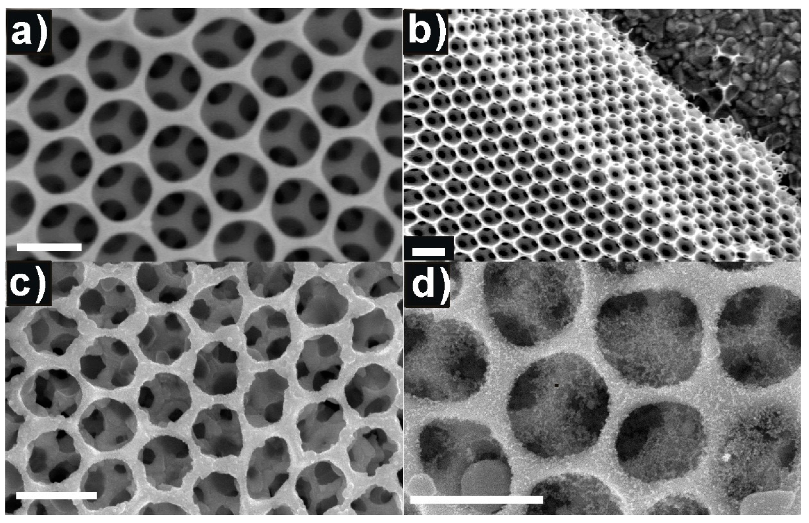
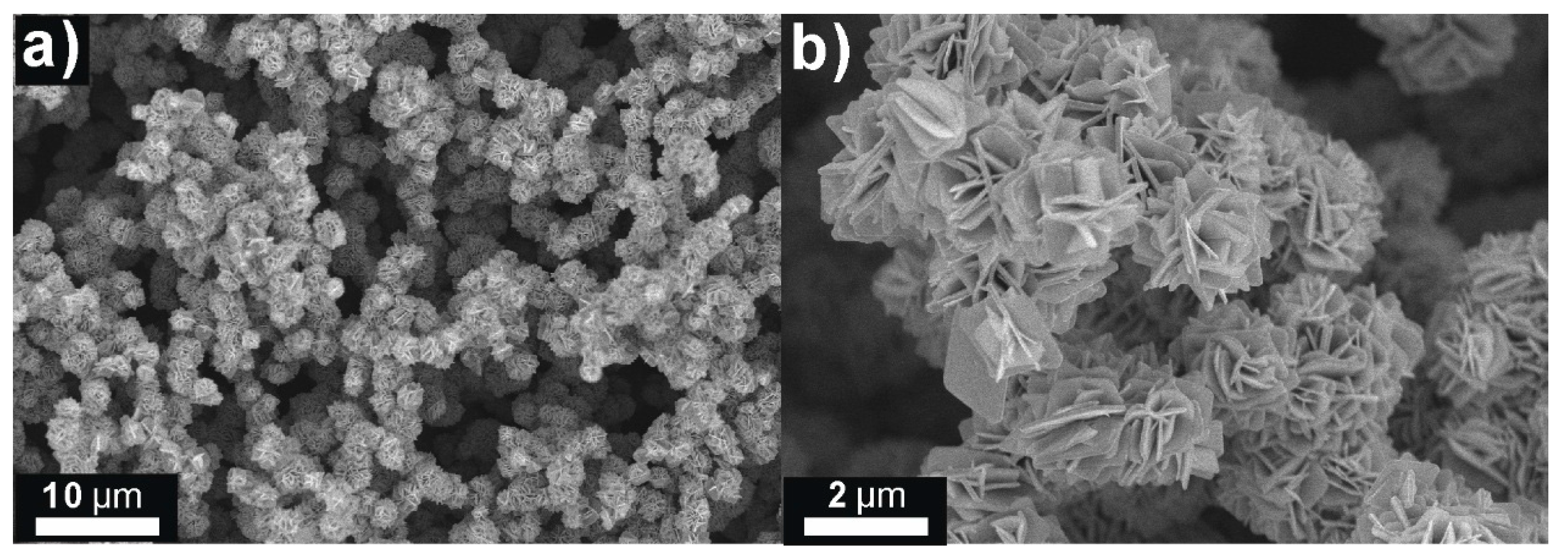
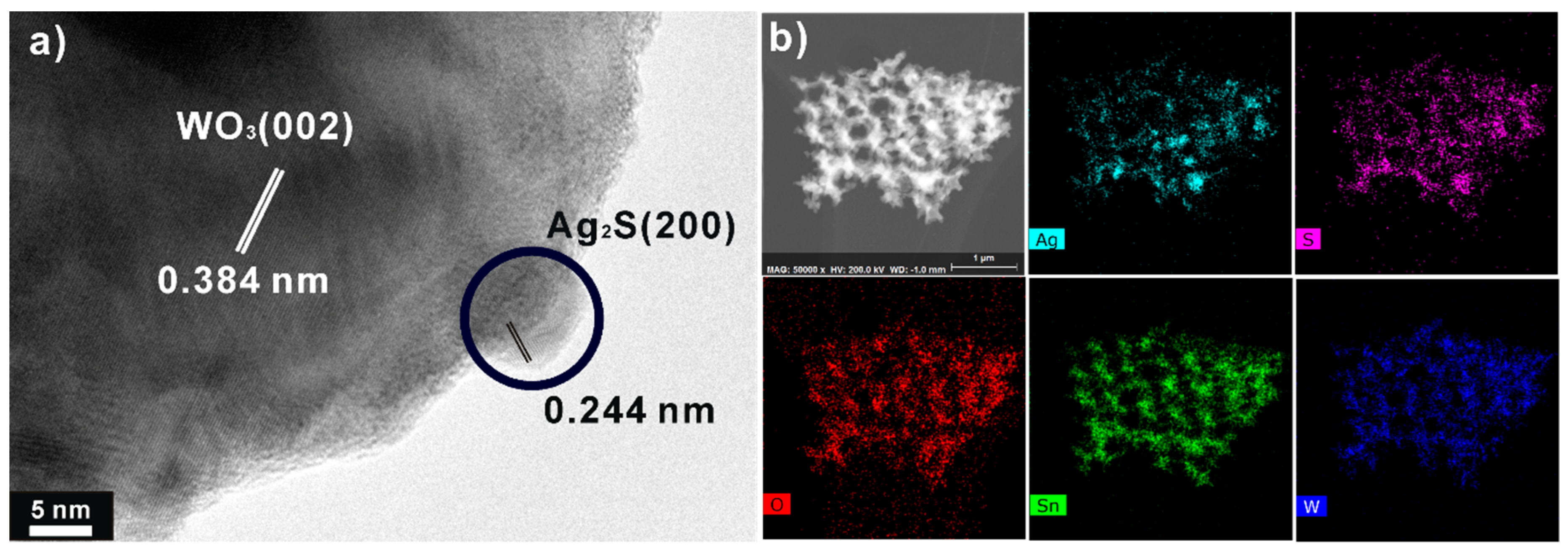
3.1. Geometrical Properties

The geometrical properties of the as-prepared PC-FTO films are initially characterized by scanning electron microscope (SEM), Figure 1a exhibits an inverse opal structural (face-centered cubic, FCC) film with the pore size of ca. 330 ± 30 nm and a smooth FTO skeleton. This PC-FTO film was fabricated on FTO glass via a well-established soft template method [34]. Figure 1b presents the edge of the as-prepared PC-FTO film, which was approximately nine layers corresponding to ca. 2 µm in thickness, indicating a large surface area available for the embedded materials, in comparison to that of planar analogs. The long-range ordered FCC array and the periodic RI (between FTO skeleton and air pore) suggests intensive photonic effects as expected by Bragg-Snell’s law. The hexagonal arrangement of the air pore corresponds to the (111) plane of an FCC structure, which is the predominant plane for the formation of a PSB from a PCs film. After the coating of WO3, homogeneous plate-like materials could be observed on the skeleton of PC-FTO (Figure 1c and Figure S1), without blocking the pores. The WO3@PC-FTO exhibits a relatively rougher surface in comparison to the bare PC-FTO (Figure 1a).
It should be noted that the amount of the embedded photoactive materials in a PC film should be carefully controlled because the excessive coating will reduce the periodicity of PCs, on the other hand, the insufficient coating may lead to weak photoresponse. Furthermore, the geometrical shape of the WO3 in a PC-FTO film can also be compared to that which is synthesized on a planar FTO substrate using the same method (Figure 2). Within PC-FTO films, the feature size of the materials can be restrained to a certain scale by the nanostructural substrate due to the complex geometrical surface, similar feature size control effects can also be found in Fe2O3 embedded SiO2 [35] or SnO2 [12] in previous reports. Figure 1d and Figure S2 reveal the WO3@PC-FTO film after the decoration of Ag2S, the Ag2S decorated samples led to rougher surface due to the relatively small crystal size of Ag2S.

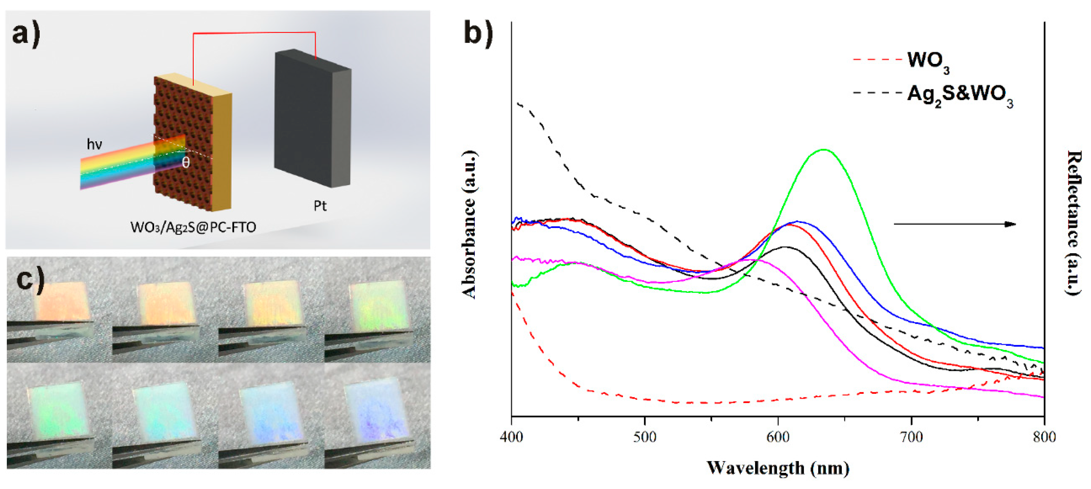
3.2. Optical Properties

Since this work was focused on the impact of photonic crystal film on the photocatalytic performance of Ag2S/WO3, the photonic effects and the optical properties of Ag2S/WO3 were characterized by diffuse reflectance UV-vis spectra (DRUVS) and UV-vis absorption spectra, respectively. The PSB position (expressed as the reflectance maximum) of PC-FTO film was recorded at the different incidence of illumination with respect to the surface normal (Figure 3a) through DRUVS. For comparison, the PSB position for (hkl) plane of a PC-FTO was also estimated by mathematic calculation from a combination of Bragg’s and Snell’s laws as the following expresses:
λ   = 2 d h k l m [ φ n 2 + ( 1 φ ) n 0 2 s i n 2 θ ] 1 2
d h k l =   D 2 [ h 2 + k 2 + l 2 ] 1 2
where φ is the filling factor of PC-FTO film (assumed to be 0.26 for FCC structure), n and n0 are the RI of FTO (ca. 1.61) and the external media, respectively. D is the periodic order of PC-FTO film (ca. 340 nm). Since the calculation of a PSB position using Bragg-Snell’s law is based on an ideal FCC structural model, thus a comparison between the calculated and experimental incident dependence of PSB can be exploited to evaluate the optical quality of the as-prepared PC-FTO film. As shown in Table S1, the experimental PSB is in good agreement with the Bragg diffraction from (111) sets of planes, in an incidence range from 15° to 45°. The PC-FTO exhibits varied PSB positions (from 585 nm to 635 nm) in the DRUVS (Figure 3b) according to the incidence of illumination. The PSB shift can also be confirmed by eye when holding the PC-FTO film at a certain angle relative to the lamp, the colors (attributed to the diffuse reflectance of PCs) varied from red to violet as shown in Figure 3c, indicating a wide tunable range of PSB positions. It should be noted that the DRUVS can hardly collect the reflected photons when there is a wide angle between sample and probe, but the photographs in Figure 3c could be evidence for the wide tunable range of the PSB.

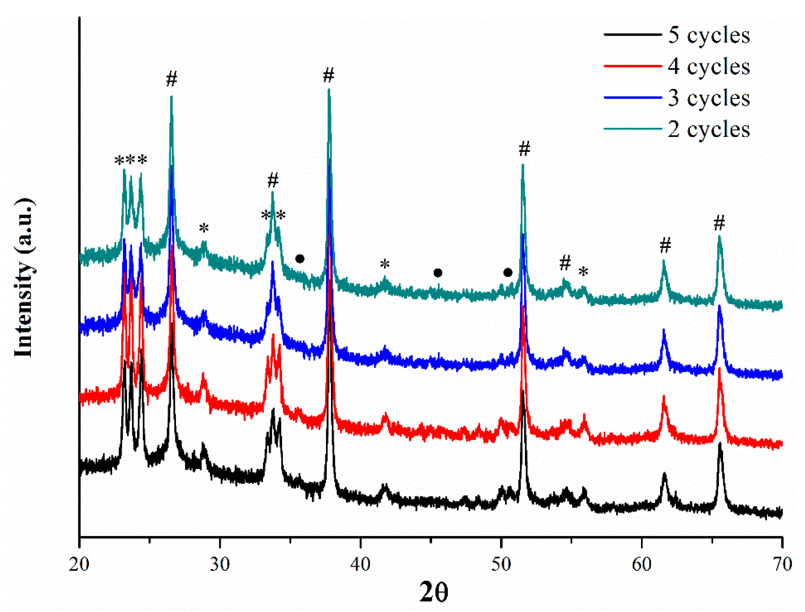
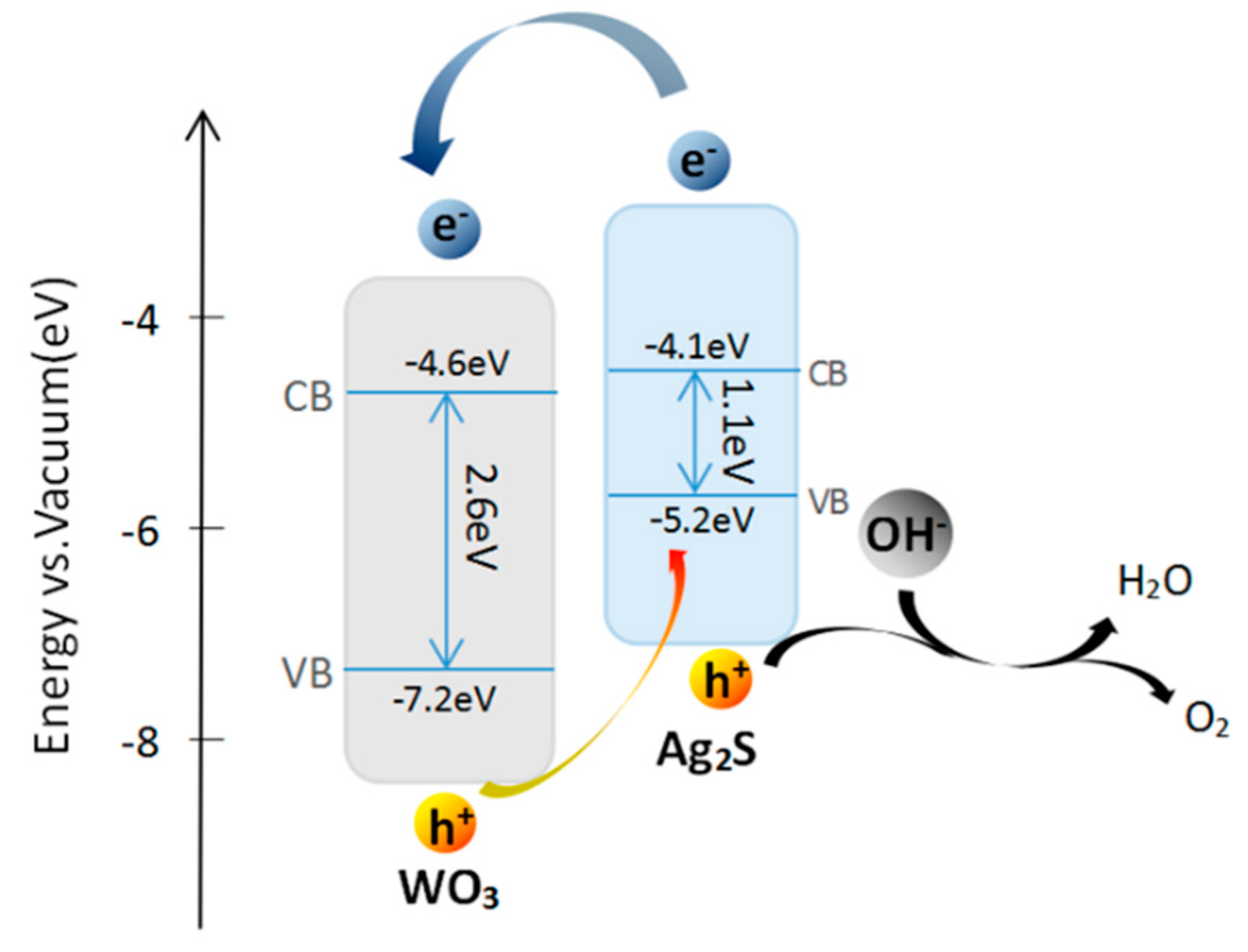
3.3. Qualitative Analysis

Figure 4a and Figure S4 reveal the high-resolution transmission electron microscopy (HR-TEM) images of the as-prepared Ag2S/WO3 on PC-FTO, the embedded WO3 platelets were attached by Ag2S (few nanometer in size), in which the lattice fringes corresponded to the (200) plane of Ag2S (JCPDS 04-0774) and the (002) crystal plane of WO3 (JCPDS 43-1034), respectively. The elemental mapping of Ag2S/WO3@PC-FTO was achieved by energy dispersive X-ray spectroscopy (EDX), from which the skeleton of PC-FTO, WO3 platelets and Ag2S dots are clearly presented in Figure 4b and Figure S3. The elemental ratio of the as-prepared Ag2S/WO3@PC-FTO sample was presented in Table S2. The powder X-ray diffraction (PXRD) was also employed for the characterization of an as-prepared Ag2S/WO3@PC-FTO, from which the diffraction patterns were consistent with the HR-TEM results. The loading amounts of Ag2S via SILAR led to no obvious difference in the PXRD patterns of samples but the slightly increased diffraction patterns from Ag2S (Figure 5).

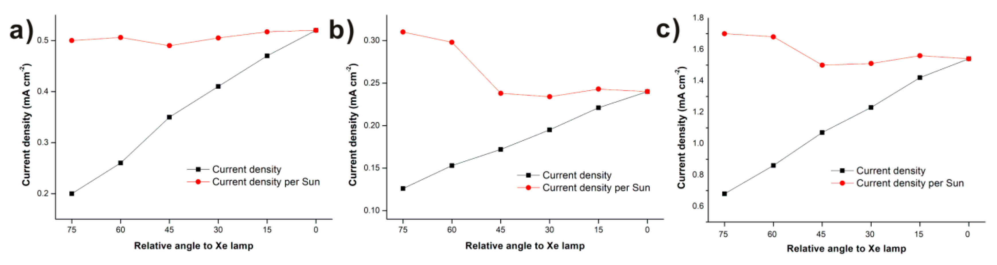
3.4. Photocatalytic Properties

Photoelectrochemistry (PEC) was exploited to evaluate the photoactivity of Ag2S/WO3@PC-FTO photoanode, as a function of incidence. The setup of a PEC cell was built up with a standard three electrode system in 1 M NaOH aqueous electrolyte, in which the sample, Pt wire, and Ag/AgCl were employed as a working electrode, counter electrode and reference electrode, respectively. The incidence of illumination was obtained by rotating the working electrode to a certain degree relative to the Xe lamp (as shown in the schematic diagram in Figure 3a). Since the rotating of electrode will lead to a reduction of received photon density (mW cm−2) by electrode, the photo density received by electrode at a certain angle was obtained by rotating a detector (shell removed) of photometer at the same angle, thus a correction (photocurrent divided by photon density received by photometer at certain angle) was conducted to evaluate the photocurrent generation under constant irradiance (1 sun, 100 mW cm−2).
Ag2S/WO3@PC-FTO electrodes of different SILAR cycles performed varied photocatalytic activities when the surface normal was illuminated, in which the 3 SILAR cycles performed the maximum photocurrent density of ca. 1.54 mA cm−2 at 0 V vs. Ag/AgCl (Figure S5) and good stability (Figure S7) in a linear sweep voltammogram (LSV), and thus this electrode was selected for the study of incidence.
For comparison, the Ag2S/WO3@planar-FTO photoanode and WO3@PC-FTO photoanode were also prepared using the same method. Due to the absence of PCs substrate, the current density generated by Ag2S/WO3@planar-FTO is ca. 32% (0.52 mA cm−2 vs. 1.54 mA cm−2) in comparison to Ag2S/WO3@PC-FTO at surface normal illumination, this is due to the lack of surface area available for the photoactive materials. The current density of Ag2S/WO3@planar-FTO was reduced 61.5% along with the incidence from 0° to 75° (Figure 6a), while the current density per sun shows no obvious variation, suggesting that the electrode could generate stable current density relative to 1 sun. In terms of the WO3@PC-FTO electrode, the current density reduced 47.6% from 0° to 75° illumination (Figure 6b). Interestingly, an obvious enhanced current density per sun was obtained at 75° and 60° illumination, where the edge of the PSB (60°) and PSB (75°) overlapped with the absorption range of WO3. Though for the Ag2S/WO3@PC-FTO electrode (Figure 6c), due the narrow band gap of Ag2S (1.1 eV, Scheme 1) [36] in visible, the PSB of PC-FTO can always overlap with the absorption range of Ag2S/WO3, and thus reducing the enhancement of current density per sun when rotating the electrode, but it still performed a slower reduction (54.5%) of current density with respect to that on planar-FTO. In theory, the PCs could suppress the recombination of charge carriers in PSB or its edge [37], and this was proved in some previous experimental reports, for instance, a 40% longer lifetime of PL decay was observed when the emission frequency of Tb3+ is close to the PSB in a PC-SiO2 system [38]. With respect for a photocatalysis system, the external media is typically aqueous (RI ≥ 1.33), and thus the RI differences between PCs materials and external media is smaller than PCs in the air (RI ≈ 1.00), which may reduce the photonic effects from PSB (Figure S6). For example, the g-C3N4 exhibited no excited state lifetime change when its absorption range overlaps with the PSB [8]. In our case, although the absorption of Ag2S/WO3 always overlapped with the PSB, we also saw no obvious PL decay lifetime enhancement. Even though, the scattering and refracting will still improve the utilization of light, when the incidence of light changes. The observed slower reduction of current density and the improved current density per sun at certain incidence suggests the realistic value of PCs.

4. Conclusions

Ag2S/WO3 and WO3 were synthesized in a PC-FTO film to demonstrate the incidence of light as a function of photocurrent density. In addition to the enhanced surface area, the embedded photoactive materials in PC-FTO perform enhanced PEC at certain incidences in comparison to that on planar analogs. Due to the multiple scattering and refracting nature of PCs, photons could be collected more effectively at certain incidence ranges (in comparison to planar analogs), resulting in enhanced photocurrent generation when integrating the product from all incidences. In consideration of the nature of sun (a changing angle light source), the results suggest that the PCs based substrate would support more efficient utilization of solar energy for the embedded photoactive materials.

Supplementary Materials

The following are available online at https://www.mdpi.com/1996-1944/12/16/2558/s1, Figure S1: SEM image of a bare WO3@mac-FTO photoanode; Figure S2: SEM images of mac-FTO film coated with only Ag2S quantum dots; Figure S3: EDX elemental mapping of Ag2S/WO3@mac-FTO with 3 SILAR cycles; Figure S4: TEM of Ag2S/WO3@PC-FTO in different magnification; Figure S5: (a) UV-vis absorption and (b) LSV of Ag2S/WO3@PC-FTO with different SILAR cycles; Figure S6: PSB spectra of PC-FTO in NaOH electrolyte; Figure S7: Stability test of Ag2S/WO3@PC-FTO electrode under illumination from surface normal for 5 min; Table S1: Calculated and experimental PSB of PC-FTO film from (111) plane; Table S2: Elemental ratios of Ag2S/WO3@PC-FTO with 3 SILAR cycles.

Author Contributions

Conceptualization, D.L.; data curation, W.W.; formal analysis, M.Y.; funding acquisition, D.L.; methodology, X.K.; project administration, M.Z.; supervision, M.Z.; writing—original draft, X.K.; writing—review and editing, M.Z.

Funding

This research was funded by the National Natural Science Foundation of China (Grant No. 61704034), the Key Platforms and Research Projects of Department of Education of Guangdong Province (Grant No. 2016KTSCX034), and the Natural Science Foundation of Guangdong Province (Grant No. 2018A0303130199 and 2017A030313632).

Conflicts of Interest

The authors declare no conflict of interest.

References

  1. Zhou, M.; Hou, Z.; Zhang, L.; Liu, Y.; Gao, Q.; Chen, X. n/n junctioned g-C3N4for enhanced photocatalytic H2generation, Sustain. Energy Fuels 2017, 1, 317–323. [Google Scholar]
  2. Zhang, M.; Robert, W.; Mitchell, H.; Huang, R.E. Douthwaite, Ordered multilayer films of hollow sphere aluminium-doped zinc oxide for photoelectrochemical solar energy conversion. J. Mater. Chem. A 2017, 5, 22193–22198. [Google Scholar] [CrossRef]
  3. Liu, H.; Wang, X.; Wu, D. Tailoring of bifunctional microencapsulated phase change materials with CdS/SiO2 double-layered shell for solar photocatalysis and solar thermal energy storage. Appl. Therm. Eng. 2018, 134, 603–614. [Google Scholar] [CrossRef]
  4. Pesci, F.M.; Sokolikova, M.S.; Grotta, C.; Sherrell, P.C.; Reale, F.; Sharda, K.; Ni, N.; Palczynski, P.; Mattevi, C. MoS2/WS2 Heterojunction for Photoelectrochemical Water Oxidation. ACS Catal. 2017, 7, 4990–4998. [Google Scholar] [CrossRef]
  5. Krbal, M.; Prikryl, J.; Zazpe, R.; Sopha, H.; Macak, J.M. CdS-coated TiO2 nanotube layers: downscaling tube diameter towards efficient heterostructured photoelectrochemical conversion. Nanoscale 2017, 9, 7755–7759. [Google Scholar] [CrossRef] [PubMed]
  6. Ye, K.-H.; Wang, Z.; Gu, J.; Xiao, S.; Yuan, Y.; Zhu, Y.; Zhang, Y.; Mai, W.; Yang, S. Carbon quantum dots as a visible light sensitizer to significantly increase the solar water splitting performance of bismuth vanadate photoanodes. Energy Environ. Sci. 2017, 10, 772–779. [Google Scholar] [CrossRef]
  7. Marandi, M.; Goudarzi, Z.; Moradi, L. Synthesis of randomly directed inclined TiO2 nanorods on the nanocrystalline TiO2 layers and their optimized application in dye sensitized solar cells. J. Alloy. Compd. 2017, 711, 603–610. [Google Scholar] [CrossRef]
  8. Qiao, S.; Mitchell, R.W.; Coulson, B.; Jowett, D.V.; Johnson, B.R.; Brydson, R.; Isaacs, M.; Lee, A.F.; Douthwaite, R.E. Douthwaite, Pore confinement effects and stabilization of carbon nitride oligomers in macroporous silica for photocatalytic hydrogen production. Carbon 2016, 106, 320–329. [Google Scholar] [CrossRef]
  9. Shuang, S.; Lv, R.; Cui, X.; Xie, Z.; Zheng, J.; Zhang, Z. Efficient photocatalysis with graphene oxide/Ag/Ag2S–TiO2 nanocomposites under visible light irradiation. RSC Adv. 2018, 8, 5784–5791. [Google Scholar] [CrossRef]
  10. Zheng, Z.; Xie, W.; Huang, B.; Dai, Y. Plasmon-Enhanced Solar Water Splitting on Metal-Semiconductor Photocatalysts. Chemistry 2018, 24, 18322–18333. [Google Scholar] [CrossRef]
  11. Nayak, A.K.; Sohn, Y.; Pradhan, D. Facile Green Synthesis of WO3·H2O Nanoplates and WO3 Nanowires with Enhanced Photoelectrochemical Performance. Cryst. Growth Des. 2017, 17, 4949–4957. [Google Scholar] [CrossRef]
  12. Xiao, Y.; Chen, M.; Zhang, M. Multiple layered macroporous SnO2 film for applications to photoelectrochemistry and morphology control of iron oxide nanocrystals. J. Power Sources 2018, 402, 62–67. [Google Scholar] [CrossRef]
  13. John, S. Strong localization of photons in certain disordered dielectric superlattices. Phys. Rev. Lett. 1987, 58, 2486–2489. [Google Scholar] [CrossRef] [PubMed] [Green Version]
  14. Yablonovitch, E. Inhibited spontaneous emission in solid-state physics and electronics. Phys. Rev. Lett. 1987, 58, 2059–2062. [Google Scholar] [CrossRef] [PubMed]
  15. Zhang, H.-F.; Liu, S.-B. Analyzing the photonic band gaps in two-dimensional plasma photonic crystals with fractal Sierpinski gasket structure based on the Monte Carlo method. AIP Adv. 2016, 6, 085116. [Google Scholar] [CrossRef] [Green Version]
  16. Zhang, H.-F. Investigations on the two-dimensional aperiodic plasma photonic crystals with fractal Fibonacci sequence. AIP Adv. 2017, 7, 075102. [Google Scholar] [CrossRef] [Green Version]
  17. Zhang, H.-F.; Chen, Y.-Q. The properties of two-dimensional fractal plasma photonic crystals with Thue-Morse sequence. Phys. Plasmas 2017, 24, 042116. [Google Scholar] [CrossRef]
  18. Zhang, L.; Lin, C.Y.; Valev, V.K.; Reisner, E.; Steiner, U.; Baumberg, J.J. Plasmonic enhancement in BiVO4 photonic crystals for efficient water splitting. Small 2014, 10, 3970–3978. [Google Scholar] [CrossRef] [PubMed]
  19. Mitchell, R.; Brydson, R.; Douthwaite, R.E. Enhancement of hydrogen production using photoactive nanoparticles on a photochemically inert photonic macroporous support. Phys. Chem. Chem. Phys. PCCP 2015, 17, 493–499. [Google Scholar] [CrossRef]
  20. Xu, Y.F.; Rao, H.S.; Chen, B.X.; Lin, Y.; Chen, H.Y.; Kuang, D.B.; Su, C.Y. Achieving Highly Efficient Photoelectrochemical Water Oxidation with a TiCl4 Treated 3D Antimony-Doped SnO2 Macropore/Branched alpha-Fe2O3 Nanorod Heterojunction Photoanode. Adv. Sci. 2015, 2, 1500049. [Google Scholar] [CrossRef]
  21. Zhu, B.; Zhang, L.; Cheng, B.; Yu, J. First-principle calculation study of tri- s -triazine-based g-C 3 N 4: A review. Appl. Catal. B Environ. 2018, 224, 983–999. [Google Scholar] [CrossRef]
  22. Cho, K.-H.; Sung, Y.-M. The formation of Z-scheme CdS/CdO nanorods on FTO substrates: The shell thickness effects on the flat band potentials. Nano Energy 2017, 36, 176–185. [Google Scholar] [CrossRef]
  23. Chen, J.I.L.; von Freymann, G.; Choi, S.Y.; Kitaev, V.; Ozin, G.A. Amplified Photochemistry with Slow Photons. Adv. Mater. 2006, 18, 1915–1919. [Google Scholar] [CrossRef]
  24. Schünemann, S.; Tüysüz, H. An Inverse Opal Structured Halide Perovskite Photocatalyst. Eur. J. Inorg. Chem. 2018, 2018, 2350–2355. [Google Scholar] [CrossRef]
  25. Cui, X.; Wang, Y.; Jiang, G.; Zhao, Z.; Xu, C.; Wei, Y.; Duan, A.; Liu, J.; Gao, J. A photonic crystal-based CdS–Au–WO3 heterostructure for efficient visible-light photocatalytic hydrogen and oxygen evolution. RSC Adv. 2014, 4, 15689–15694. [Google Scholar] [CrossRef]
  26. Xiao, Y.; Chen, M.; Zhang, M. Improved utilization of sun light through the incidence dependence of photonic stop band: g-C3N4 embedded FTO photonic crystal film. ChemPhotoChem 2018, 3, 101–106. [Google Scholar] [CrossRef]
  27. Lin, S.; Feng, Y.; Wen, X.; Harada, T.; Kee, T.W.; Huang, S.; Shrestha, S.; Conibeer, G. Observation of Hot Carriers Existing in Ag2S Nanoparticles and Its Implication on Solar Cell Application. J. Phys. Chem. C 2016, 120, 10199–10205. [Google Scholar] [CrossRef]
  28. Tubtimtae, A.; Wu, K.-L.; Tung, H.-Y.; Lee, M.-W.; Wang, G.J. Ag2S quantum dot-sensitized solar cells. Electrochem. Commun. 2010, 12, 1158–1160. [Google Scholar] [CrossRef]
  29. Park, K.-H.; Dhayal, M. Simultaneous growth of rutile TiO2 as 1D/3D nanorod/nanoflower on FTO in one-step process enhances electrochemical response of photoanode in DSSC. Electrochem. Commun. 2014, 49, 47–50. [Google Scholar] [CrossRef]
  30. Wu, J.-J.; Chang, R.-C.; Chen, D.-W.; Wu, C.-T. Visible to near-infrared light harvesting in Ag2S nanoparticles/ZnO nanowire array photoanodes. Nanoscale 2012, 4, 1368. [Google Scholar] [CrossRef]
  31. Shen, H.; Jiao, X.; Oron, D.; Li, J.; Lin, H. Efficient electron injection in non-toxic silver sulfide (Ag2S) sensitized solar cells. J. Power Sources 2013, 240, 8–13. [Google Scholar] [CrossRef]
  32. Tubtimtae, A.; Cheng, K.-Y.; Lee, M.-W. Ag2S quantum dot-sensitized WO3 photoelectrodes for solar cells. J. Solid State Electrochem. 2014, 18, 1627–1633. [Google Scholar] [CrossRef]
  33. Wang, W.; Dong, J.; Ye, X.; Li, Y.; Ma, Y.; Qi, L. Heterostructured TiO2 Nanorod@Nanobowl Arrays for Efficient Photoelectrochemical Water Splitting. Small 2016, 12, 1469–1478. [Google Scholar] [CrossRef] [PubMed]
  34. Xie, H.; Li, Y.; Jin, S.; Han, J.; Zhao, X. Facile Fabrication of 3D-Ordered Macroporous Nanocrystalline Iron Oxide Films with Highly Efficient Visible Light Induced Photocatalytic Activity. J. Phys. Chem. C 2010, 114, 9706–9712. [Google Scholar] [CrossRef]
  35. Brillet, J.; Gratzel, M.; Sivula, K. Decoupling feature size and functionality in solution-processed, porous hematite electrodes for solar water splitting. Nano Lett. 2010, 10, 4155–4160. [Google Scholar] [CrossRef] [PubMed]
  36. Hou, W.; Xiao, Y.; Han, G.; Zhang, Y.; Chang, Y. Titanium dioxide/zinc indium sulfide hetero-junction: An efficient photoanode for the dye-sensitized solar cell. J. Power Sources 2016, 328, 578–585. [Google Scholar] [CrossRef]
  37. Sakoda, K. Enhanced light amplification due to group-velocity anomaly peculiar to two- and three-dimensional photonic crystals. Opt. Express 1999, 4, 167–176. [Google Scholar] [CrossRef]
  38. Aloshyna, M.; Sivakumar, S.; Venkataramanan, M.; Brolo, A.G.; van Veggel, F.C.J.M. Significant Suppression of Spontaneous Emission in SiO2 Photonic Crystals Made with Tb3+-Doped LaF3Nanoparticles. J. Phys. Chem. C 2007, 111, 4047–4051. [Google Scholar] [CrossRef]
Figure 1. (a) SEM image of macroporous fluorine-doped tin oxide with photonic crystal structure (PC-FTO) viewed perpendicularly; (b) SEM image of the edge of PC-FTO film; (c) SEM image of WO3@PC-FTO; (d) SEM image of Ag2S/WO3@PC-FTO, scale bar = 500 nm.
Materials 12 02558 g001
Figure 2. SEM images of WO3 synthesized on planar FTO glass. (a) SEM of WO3 of low magnification; (b) SEM of WO3 of high magnification.
Materials 12 02558 g002
Figure 3. (a) Schematic diagram of the varied incidence illumination on a PC-FTO based electrode. (b) diffuse reflectance UV-vis spectra (DRUVS) (solid line) of photonic stop band (PSB) positions under different incidence and UV-vis absorption spectra (dash line) of WO3 and Ag2S/WO3. (c) digital photographs of one PC-FTO film under different incidences.
Materials 12 02558 g003
Figure 4. (a) high-resolution transmission electron microscopy (HR-TEM) image of Ag2S/WO3@PC-FTO photoanode; (b) TEM-EDX elemental mapping of Ag2S/WO3@PC-FTO.
Materials 12 02558 g004
Figure 5. Powder X-ray diffraction (PXRD) of Ag2S/WO3@PC-FTO electrode with different loading of Ag2S, * = WO3, # = SnO2 and • = Ag2S.
Materials 12 02558 g005
Figure 6. Incidence dependence of photoelectrochemistry (PEC) current density and current density relative to 1 sun (ca. 100 mW cm−2) for (a) Ag2S/WO3@planar-FTO; (b) WO3@PC-FTO and (c) Ag2S/WO3@PC-FTO at 0 V vis VAg/AgCl, the irradiance to the surface normal is adjusted to 1 sun.
Materials 12 02558 g006
Scheme 1. Mechanism of Ag2S decorated WO3 under illumination.
Materials 12 02558 sch001

