A Study of Quantum Confinement Effects in Ultrathin NiO Films Performed by Experiment and Theory


 , ,
, , 
Abstract
:
1. Introduction
2. Materials and Methods
2.1. Experimental Details
2.2. Theory
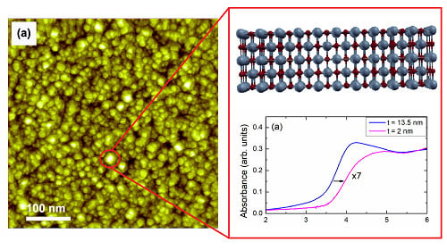
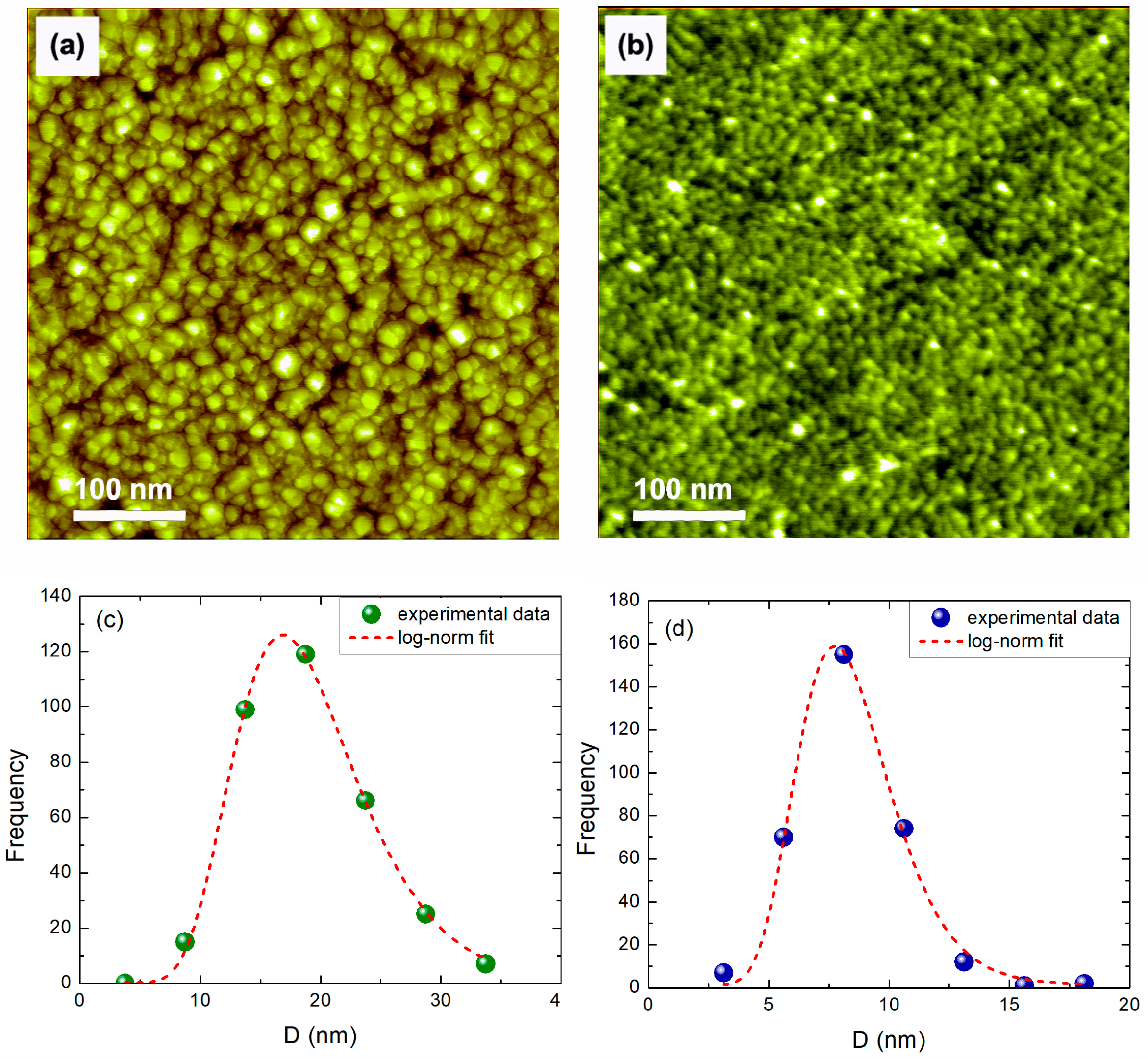
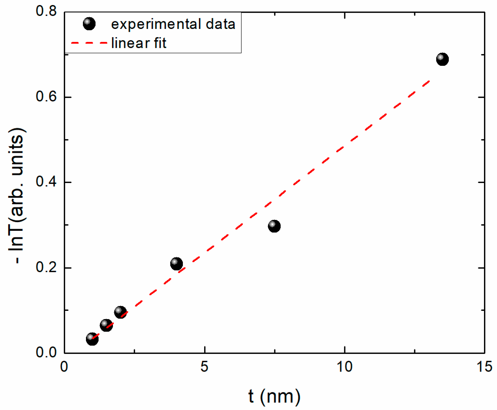
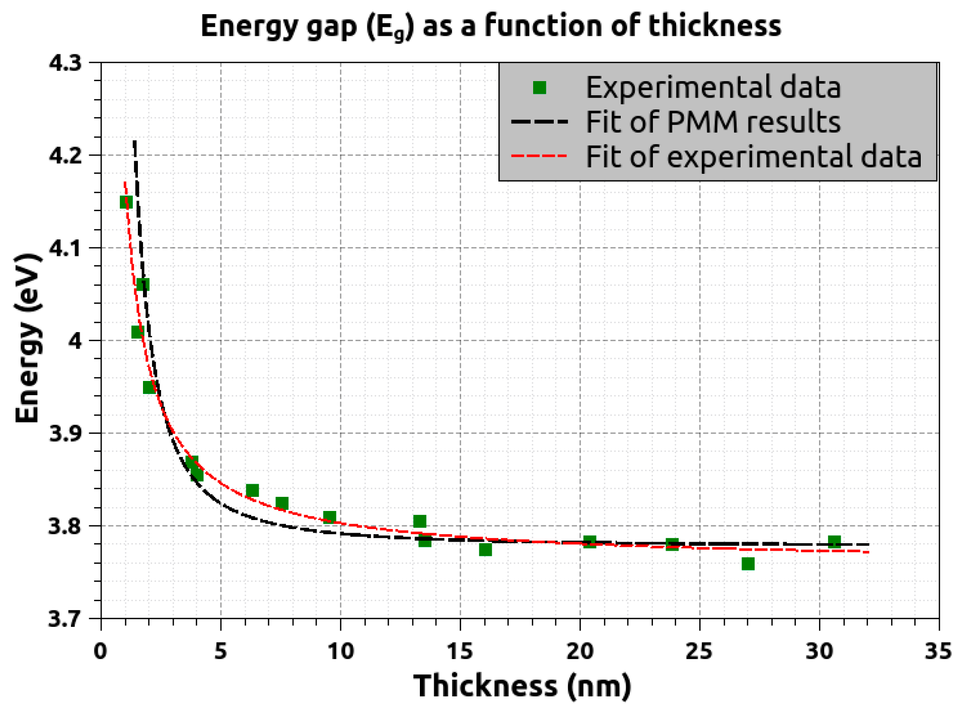
3. Results
3.1. Grain Growth
3.2. Optical Properties
4. Discussion and Conclusions
Author Contributions
Funding
Conflicts of Interest
References
- Powell, J.; Spicer, W.E. Optical Properties of NiO and CoO. Phys. Rev. B 1970, 2, 2182–2193. [Google Scholar] [CrossRef]
- Hotovy, I.; Rehacek, V.; Siciliano, P.; Capone, S.; Spiess, L. Sensing characteristics of NiO thin films as NO2 gas sensor. Thin Solid Films 2002, 418, 9–15. [Google Scholar] [CrossRef]
- Wang, J.; Yang, P.; Wei, X.; Zhou, Z. Nano- and mesoscale modeling of cement matrix. Nanoscale Res. Lett. 2015, 10, 173. [Google Scholar] [CrossRef]
- Wang, H.; Zou, C.; Zhou, L.; Tian, C.; Fu, D. Resistive switching characteristics of thin NiO film based flexible nonvolatile memory devices. Microelectron. Eng. 2012, 91, 144–146. [Google Scholar] [CrossRef]
- Bogner, M.; Fuchs, A.; Scharnagl, K.; Winter, R.; Doll, T.; Eisele, I. Thin (NiO)1−x(Al2O3)x, Al doped and Al coated NiO layers for gas detection with HSGFET. Sens. Actuators B Chem. 1998, 47, 145–152. [Google Scholar] [CrossRef]
- Ohta, H.; Hosono, H. Transparent oxide optoelectronics. Mater. Today 2004, 7, 42–51. [Google Scholar] [CrossRef]
- Irwin, M.D.; Buchholz, D.B.; Hains, A.W.; Chang, R.P.H.; Marks, T.J. P-Type semiconducting nickel oxide as an efficiency-enhancing anode interfacial layer in polymer bulk-heterojunction solar cells. Proc. Natl. Acad. Sci. USA 2008, 105, 2783–2787. [Google Scholar] [CrossRef]
- Park, J.H.; Seo, J.; Park, S.; Shin, S.S.; Kim, Y.C.; Jeon, N.J.; Shin, H.; Ahn, T.K.; Noh, J.H.; Yoon, S.C.; et al. Efficient CH3NH3PbI3 perovskite solar cells employing nanostructured p-type NiO electrode formed by a pulsed laser deposition. Adv. Mater. 2015, 27, 4013–4019. [Google Scholar] [CrossRef] [PubMed]
- Chrissanthopoulos, A.; Baskoutas, S.; Bouropoulos, N.; Dracopoulos, V.; Poulopoulos, P.; Yannopoulos, S.N. Synthesis and characterization of ZnO/NiO p-n heterojunctions: ZnO nanorods grown on NiO thin film by thermal evaporation. Photonics Nanostruct. 2011, 9, 132–139. [Google Scholar] [CrossRef]
- Dewan, S.; Tomar, M.; Tandon, R.P.; Gupta, V. Zn doping induced conductivity transformation in NiO films for realization of p-n homo junction diode. J. Appl. Phys. 2017, 121, 215307–215316. [Google Scholar] [CrossRef]
- Chen, L.; Shet, S.; Tang, H.; Ahn, K.; Wang, H.; Yan, Y.; Turner, J.; Al-Jassim, M. Amorphous copper tungsten oxide with tunable band gaps. J. Appl. Phys. 2010, 108, 043502. [Google Scholar] [CrossRef]
- Baskoutas, S.; Poulopoulos, P.; Karoutsos, V.; Angelakeris, M.; Flevaris, N.K. Strong quantum confinement effects in thin zinc selenide films. Chem. Phys. Lett. 2006, 417, 461–464. [Google Scholar] [CrossRef]
- Sawaby, A.; Selim, M.S.; Marzouk, S.Y.; Mostafa, M.A.; Hosny, A. Structure, optical and electrochromic properties of NiO thin films. Physica B 2010, 405, 3412–3420. [Google Scholar] [CrossRef]
- Subramanian, B.; Mohamed Ibrahim, M.; Senthilkumar, V.; Murali, K.R.; Vidhya, V.S. Optoelectronic and electrochemical properties of nickel oxide (NiO) films deposited by DC reactive magnetron sputtering. Physica B 2008, 403, 4104–4110. [Google Scholar] [CrossRef]
- Ush, K.S.; Sivakumar, R.; Sanjeeviraja, C. Optical constants and dispersion energy parameters of NiO thin films prepared by radio frequency magnetron sputtering technique. J. Appl. Phys. 2013, 114, 123501–123511. [Google Scholar] [CrossRef]
- Jiang, D.Y.; Qin, J.M.; Wang, X.; Gao, S.; Liang, Q.C.; Zhao, J.X. Optical properties of NiO thin films fabricated by electron beam evaporation. Vacuum 2012, 86, 1083–1086. [Google Scholar] [CrossRef]
- Pappas, S.D.; Grammatikopoulos, S.; Poulopoulos, P.; Trachylis, D.; Velgakis, M.J.; Politis, C. Growth and Optical Properties of Thin NiO Films. J. Surf. Interfaces Mater. 2014, 2, 233–237. [Google Scholar] [CrossRef]
- Grammatikopoulos, S.; Stamatelatos, A.; Delimitis, A.; Sousanis, A.; Chrisanthopoulou, A.; Trachylis, D.; Politis, C.; Poulopoulos, P. Growth of Au Nanoparticles in NiO via Short Annealing of Precursor Material Thin Film and Optimization of Plasmonics. Phys. Status Solidi A 2017, 214, 1700303–1700309. [Google Scholar] [CrossRef]
- Fasaki, I.; Koutoulaki, A.; Kompitsas, M.; Charitidis, C. Structural, electrical and mechanical properties of NiO thin films grown by pulsed laser deposition. Appl. Surf. Sci. 2010, 257, 429–433. [Google Scholar] [CrossRef]
- Fox, M. Optical Properties of Solids, 2nd ed.; Oxford University Press: New York, NY, USA, 2010; ISBN 9780199573370. [Google Scholar]
- Rieth, M.; Schommers, W.; Baskoutas, S. Exact numerical solution of Schroedinger’s equation for a particle in an interaction potential of general shape. Int. J. Mod. Phys. B 2002, 16, 4081–4092. [Google Scholar] [CrossRef]
- Baskoutas, S.; Terzis, A.F.J. Size-dependent band gap of colloidal quantum dots. J. Appl. Phys. 2006, 99, 013708–013712. [Google Scholar] [CrossRef]
- Baskoutas, S.; Terzis, A.F.; Schommers, W. Size-dependent exciton energy of narrow band gap colloidal quantum dots in the finite depth square-well effective mass approximation. J. Comp. Theor. Nanosci. 2006, 3, 269–271. [Google Scholar] [CrossRef]
- Li, L.; Kanai, Y. Antiferromagnetic structures and electronic energy levels at reconstructed NiO(111) surfaces: A DFT + U study. Phys. Rev. B 2015, 91, 235304–235313. [Google Scholar] [CrossRef]
- Messiah, A. Quantum Mechanics; North-Holland: Amsterdam, The Netherlands, 1966; Volume II. [Google Scholar]
- Sato, H.; Minami, T.; Takata, S.; Yamada, T. Transparent conducting p-type NiO thin films prepared by magnetron sputtering. Thin Solid Films 1993, 236, 27–31. [Google Scholar] [CrossRef]
- Irwin, M.D.; Servaites, J.D.; Buchholz, D.; Leever, B.J.; Liu, J.; Emery, J.D.; Zhang, M.; Song, J.-H.; Durstock, M.F.; Freeman, A.J.; et al. Structural and electrical functionality of NiO interfacial films in bulk heterojunction organic solar cells. Chem. Mater. 2011, 23, 2218–2226. [Google Scholar] [CrossRef]
- Garoufalis, C.S.; Poulopoulos, P.; Bouropoulos, N.; Barnasas, A.; Baskoutas, S. Growth and optical properties of Fe2O3 thin films: A study of quantum confinement effects by experiment and theory. Physica E 2017, 89, 67–71. [Google Scholar] [CrossRef]
- Karoutsos, V. Scanning probe microscopy: Instrumentation and applications on thin films and magnetic multilayers. J. Nanosci. Nanotechnol. 2009, 9, 6783–6798. [Google Scholar] [CrossRef] [PubMed]
- Peng, H.; Lany, S. Semiconducting transition-metal oxides based on d5 cations: Theory for MnO and Fe2O3. Phys. Rev. B 2012, 85, 201202–201207. [Google Scholar] [CrossRef]
- Escobar, M.A.; Magana, L.F.; Valenzuela, R. Effect of the grain size distribution on the magnetization curve. J. Appl. Phys. 1985, 57, 2142–2147. [Google Scholar] [CrossRef]
- Srolovitz, D.J. Grain growth phenomena in films: A Monte Carlo approach. J. Vac. Sci. Technol. A 1986, 4, 2925–2930. [Google Scholar] [CrossRef]
- Karoutsos, V.; Papasotiriou, P.; Poulopoulos, P.; Kapaklis, V.; Politis, C.; Angelakeris, M.; Kehagias, T.; Flevaris, N.K.; Papaioannou, E.T. Growth modes of nanocrystalline Ni/Pt multilayers with deposition temperature. J. Appl. Phys. 2007, 102, 043525–0435344. [Google Scholar] [CrossRef]
- Karoutsos, V.; Toudas, M.; Delimitis, A.; Grammatikopoulos, S.; Poulopoulos, P. Microstructural evolution in nanostructured gold films. Thin Solid Films 2012, 520, 4074–4079. [Google Scholar] [CrossRef]
- Zöllner, D. Treating grain growth in thin films in three dimensions: A simulation study. Comput. Mater. Sci. 2016, 125, 51–60. [Google Scholar] [CrossRef]
- Atkinson, H.V. Theories of normal grain growth in pure single phase systems. Acta Metall. 1988, 36, 469–491. [Google Scholar] [CrossRef]
- Song, X.; Liu, G. Computer simulation of normal grain growth in polycrystalline thin films. J. Mater. Sci. 1999, 34, 2433–2436. [Google Scholar] [CrossRef]
- Zhang, J.; Adams, J.B. Modeling and visualization of polycrystalline thin film growth. Comput. Mater. Sci. 2004, 31, 317–328. [Google Scholar] [CrossRef]
- Paritosh; Srolovitz, D.J.; Battaile, C.C.; Li, X.; Butler, J.E. Simulation of faceted film growth in two-dimensions: Microstructure, morphology and texture. Acta Mater. 1999, 47, 2269–2281. [Google Scholar] [CrossRef]
- Premkumar, P.A.; Delabie, A.; Rodriguez, L.N.J.; Moussa, A.; Adelmann, C. Roughness evolution during the atomic layer deposition of metal oxides. J. Vac. Sci. Technol. A 2013, 31, 061501–061506. [Google Scholar] [CrossRef]
- Singh, P.; Chawla, A.K.; Kaur, D.; Chandra, R. Effect of oxygen partial pressure on the structural and optical properties of sputter deposited ZnO nanocrystalline thin films. Mater. Lett. 2007, 61, 2050–2053. [Google Scholar] [CrossRef]
- Seung, C.C.; Koumoto, K.; Hiroaki, Y. Electrical conduction and effective mass of a hole in single-crystal NiO. J. Mater. Sci. 1986, 21, 1947–1950. [Google Scholar] [CrossRef]
- Osburn, C.M.; Vest, R.W. Defect structure and electrical properties of NiO—I. High temperature. J. Phys. Chem. Solids 1971, 32, 1331–1342. [Google Scholar] [CrossRef]
- Wilson, T.M. A study of the electronic structure of the first-row transition-metal compounds. Int. J. Quantum Chem. 1969, 4, 757–774. [Google Scholar] [CrossRef]
- Hanken, H. Kopplung nichtrelativistischer teilchen mit einem quantisierten feld. Nuovo Cim. 1956, 3, 1230–1253. [Google Scholar] [CrossRef]
- Mochizuki, S. Radiative optical modes of vibration in NiO thin film. Phys. Status Solidi B 1984, 126, 105–114. [Google Scholar] [CrossRef]
- Lacerda, M.M.; Kargar, F.; Aytan, E.; Samnakay, R.; Debnath, B.; Li, J.X.; Khitun, A.; Lake, R.K.; Shi, J.; Balandin, A.A. Variable-temperature inelastic light scattering spectroscopy of nickel oxide: Disentangling phonons and magnons. Appl. Phys. Lett. 2017, 110, 202406–202410. [Google Scholar] [CrossRef]


© 2018 by the authors. Licensee MDPI, Basel, Switzerland. This article is an open access article distributed under the terms and conditions of the Creative Commons Attribution (CC BY) license (http://creativecommons.org/licenses/by/4.0/).
Share and Cite
Garoufalis, C.S.; Barnasas, A.; Stamatelatos, A.; Karoutsos, V.; Grammatikopoulos, S.; Poulopoulos, P.; Baskoutas, S. A Study of Quantum Confinement Effects in Ultrathin NiO Films Performed by Experiment and Theory. Materials 2018, 11, 949. https://doi.org/10.3390/ma11060949
Garoufalis CS, Barnasas A, Stamatelatos A, Karoutsos V, Grammatikopoulos S, Poulopoulos P, Baskoutas S. A Study of Quantum Confinement Effects in Ultrathin NiO Films Performed by Experiment and Theory. Materials. 2018; 11(6):949. https://doi.org/10.3390/ma11060949
Chicago/Turabian StyleGaroufalis, Christos S., Alexandros Barnasas, Alkeos Stamatelatos, Vagelis Karoutsos, Spyridon Grammatikopoulos, Panagiotis Poulopoulos, and Sotirios Baskoutas. 2018. "A Study of Quantum Confinement Effects in Ultrathin NiO Films Performed by Experiment and Theory" Materials 11, no. 6: 949. https://doi.org/10.3390/ma11060949