Article

Spin Polarization Properties of Pentagonal PdSe2 Induced by 3D Transition-Metal Doping: First-Principles Calculations

1
School of Physics and Electronics, Shandong Normal University, Jinan 250014, China
2
Institute of Materials and Clean Energy, Shandong Normal University, Jinan 250014, China
*
Authors to whom correspondence should be addressed.
Materials 2018, 11(11), 2339; https://doi.org/10.3390/ma11112339
Submission received: 24 October 2018 / Revised: 15 November 2018 / Accepted: 19 November 2018 / Published: 21 November 2018

Abstract

:
The electronic structure and spin polarization properties of pentagonal structure PdSe2 doped with transition metal atoms are studied through first- principles calculations. The theoretical investigations show that the band gap of the PdSe2 monolayer decreases after introducing Cr, Mn, Fe and Co dopants. The projected densities of states show that p-d orbital couplings between the transition metal atoms and PdSe2 generate new spin nondegenerate states near the Fermi level which make the system spin polarized. The calculated magnetic moments, spin density distributions and charge transfer of the systems suggest that the spin polarization in Cr-doped PdSe2 will be the biggest. Our work shows that the properties of PdSe2 can be modified by doping transition metal atoms, which provides opportunity for the applications of PdSe2 in electronics and spintronics.

Graphical Abstract

1. Introduction

The successful stripping of graphene has greatly stimulated people’s interest in the research of two-dimensional (2D) materials, and it has been widely used in the design of electronic devices due to its remarkable physical and chemical properties [1,2,3,4,5]. However, the zero band gap of graphene limits its application in electronics, which leads to the emergence of other 2D materials with a hexagonal structure beyond graphene, such as black phosphorous, boron nitride and transition metal di-chalcogenides (TMDCs) [6,7,8,9,10,11,12,13]. Two-dimensional hexagonal structure materials are widely used in various aspects, especially in spintronics. The long spin-coherence lengths and high spin-orbit coupling offer more opportunities for the fabrication of 2D spintronic devices, such as graphene nanoribbon electrodes, graphene spin valve, MoS2 switching of spin currents and so on [14,15]. Researching and inducing magnetic structures of 2D materials are vital but challenging topics in 2D spintronic devices. Various strategies to obtain magnetism have been performed, such as the introduction of defects [16,17], electric field and strain modulation [18,19], 3D transition-metal (TM) atom doping [20,21], surface adsorption [22,23,24], doping combined with adsorption [25] and so on.
With the tremendous efforts in research, more novel 2D materials came out. For example, a new class of layered material formed by noble metals (e.g., Pd and Pt) with S or Se atoms has been extensively investigated in recent years [26,27,28]. In fact, the hexagonal structure is the dominant motif in the ocean of 2D material. However, there is still a lack of experimental studies on the pentagonal structure. Recently, novel 2D PdSe2 composed of a pentagonal structure has been successfully exfoliated by Oyedele, et al., which provides exciting opportunities for the research of pentagonal 2D materials [29]. PdSe2 is a new material, it has strong-interlayer coupling [30,31], in addition, the air-stability and anisotropy of PdSe2 have been proved, moreover, few-layer PdSe2 behaves ambipolar semiconducting, with high electron-apparent field-effect mobility. Furthermore, the monolayer PdSe2 has an indirect band gap of about 1.3 eV, while the band gap of bulk PdSe2 is about 0 eV, hence the band gap of PdSe2 can be tuned between 0–1.3 eV, this is different from that in MoS2 with a value between 1.2–1.8 eV [28].
Compared with previously realized isotropic planar structures, the unique atomic configuration, coupled with the buckling structure, result in exotic mechanical properties, with an unusual negative Poisson’s ratio and ultrahigh mechanical strength. The spin-orbit coupling is strong, and a topological quantum phase transition also can be tuned in PdSe2. Therefore, the PdSe2 is a favorable candidate for designing novel 2D spintronic devices [29,32]. However, pristine PdSe2 is nonmagnetic, which will hinder its usage in spintronic devices. Recently, the half-metallic ferromagnetism of PdSe2 monolayer with hole-doping under uniaxial stress has been investigated by Zhang, et al. [33], which shows that Stoner ferromagnetism can be induced through hole-doping. In this paper, we studied the magnetic properties of PdSe2 with 3D TM atom dopants (Cr, Mn, Fe, Co and Ni atoms) by means of first-principles calculations.

2. Theoretical Model and Computational Details

In our first-principles calculations, we adopt the Vienna Ab Initio Simulation Package (VASP) equipped with the projector-augmented-wave (PAW) method to study the electron-ion interactions [34]. The Perdew-Burke-Ernzerh (PBE) functional of the generalized gradient approximation (GGA) is considered to treat the electron exchange correlation, which produces the correct ground-state structure of the combined systems [35,36,37]. In our calculations, the model of the 2 × 2 × 1 pristine single-layer PdSe2 (24 atoms) is given, the distance between adjacent PdSe2 layer set as 20 Å to avoid the effects induced by periodic boundary conditions. The Brillouin zone sampling uses a 11 × 11 × 1 Monkhorst-Pack grid. To reach a convergence of the total energy, the cut-off energy with 400 eV has been adopted in each calculation. The convergence threshold of the residual forces on each atom is 0.01 eV/Å and the total energy changes are less than 10−4 eV. The layers of PdSe2 are mainly held together by van der Waals forces [29,38], therefore, van der Waals (vdW) is introduced in the density functional method.

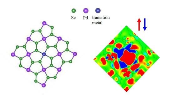
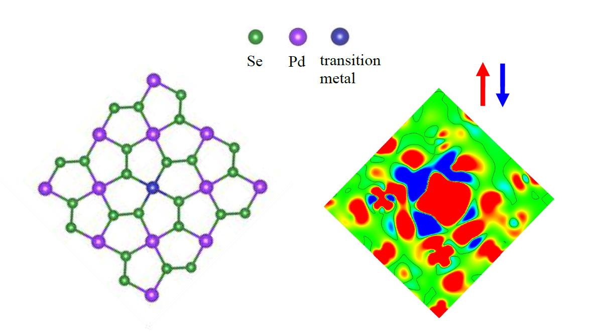
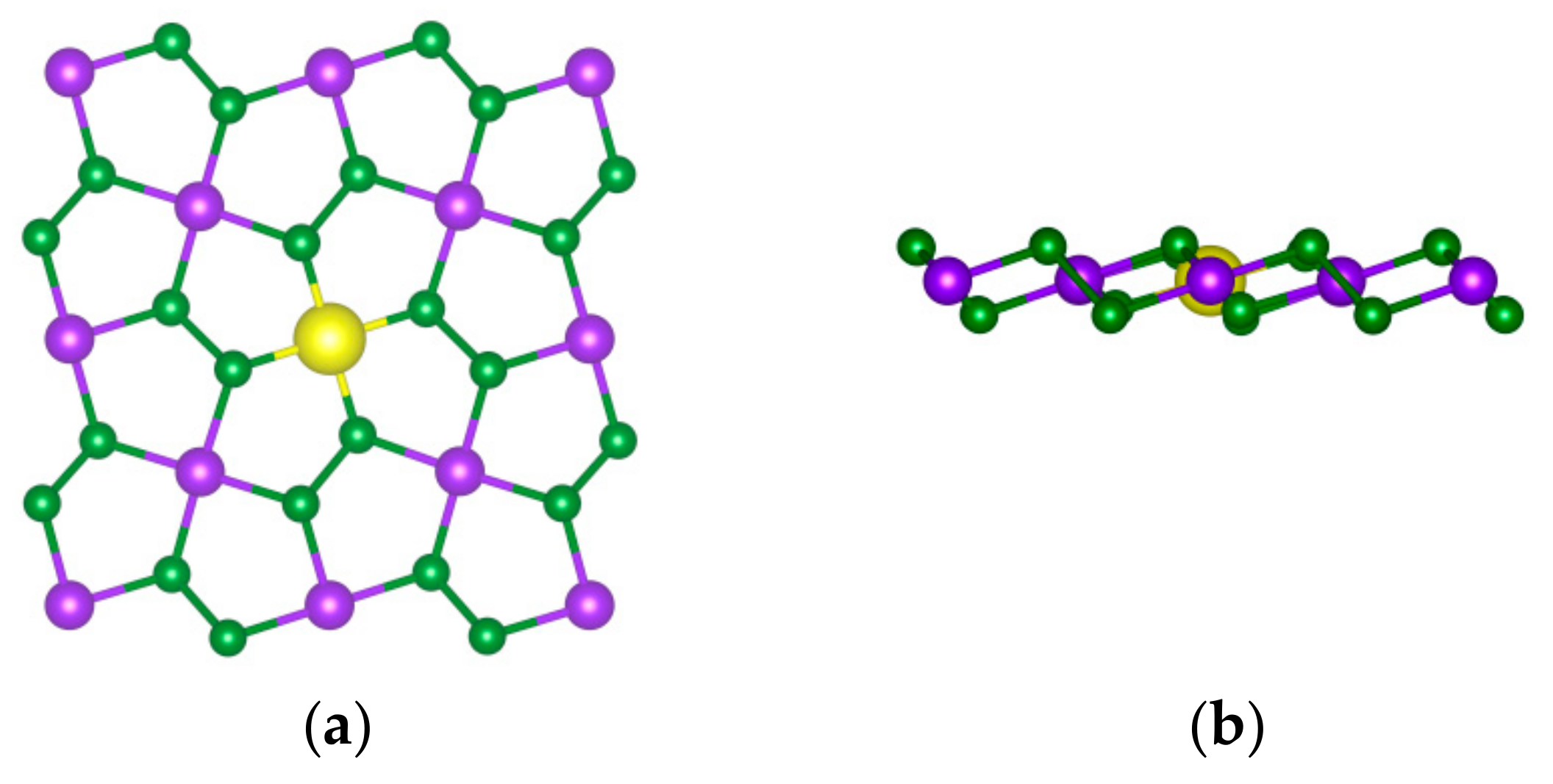
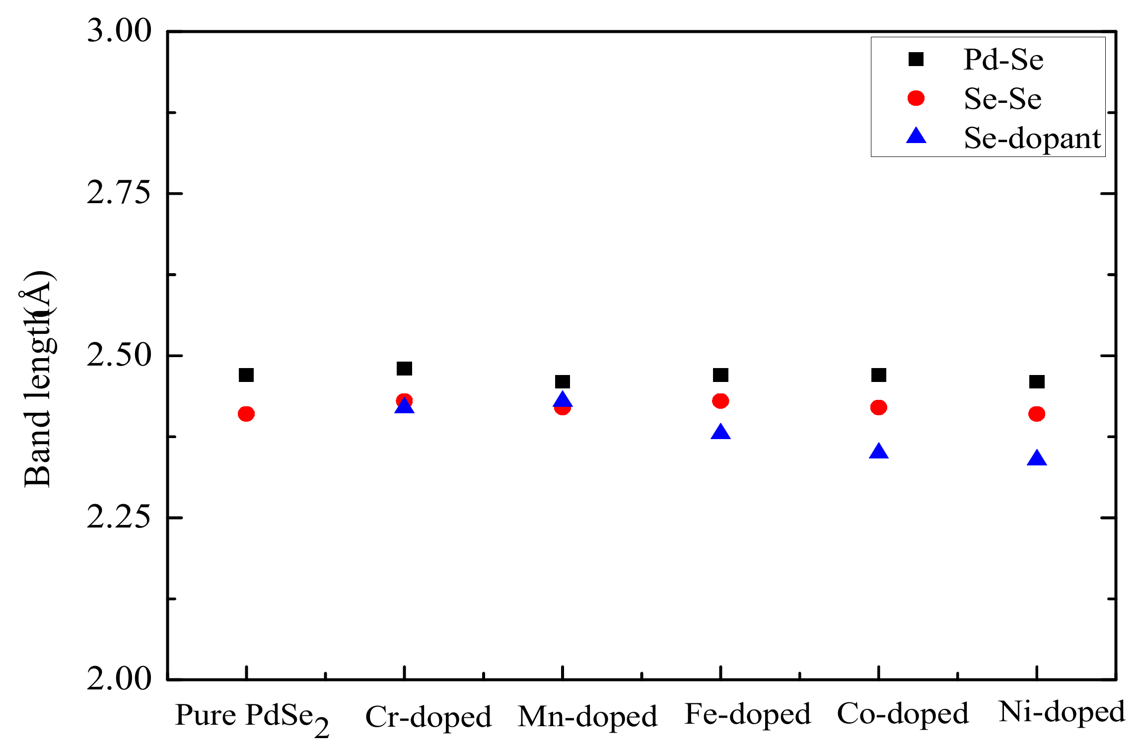
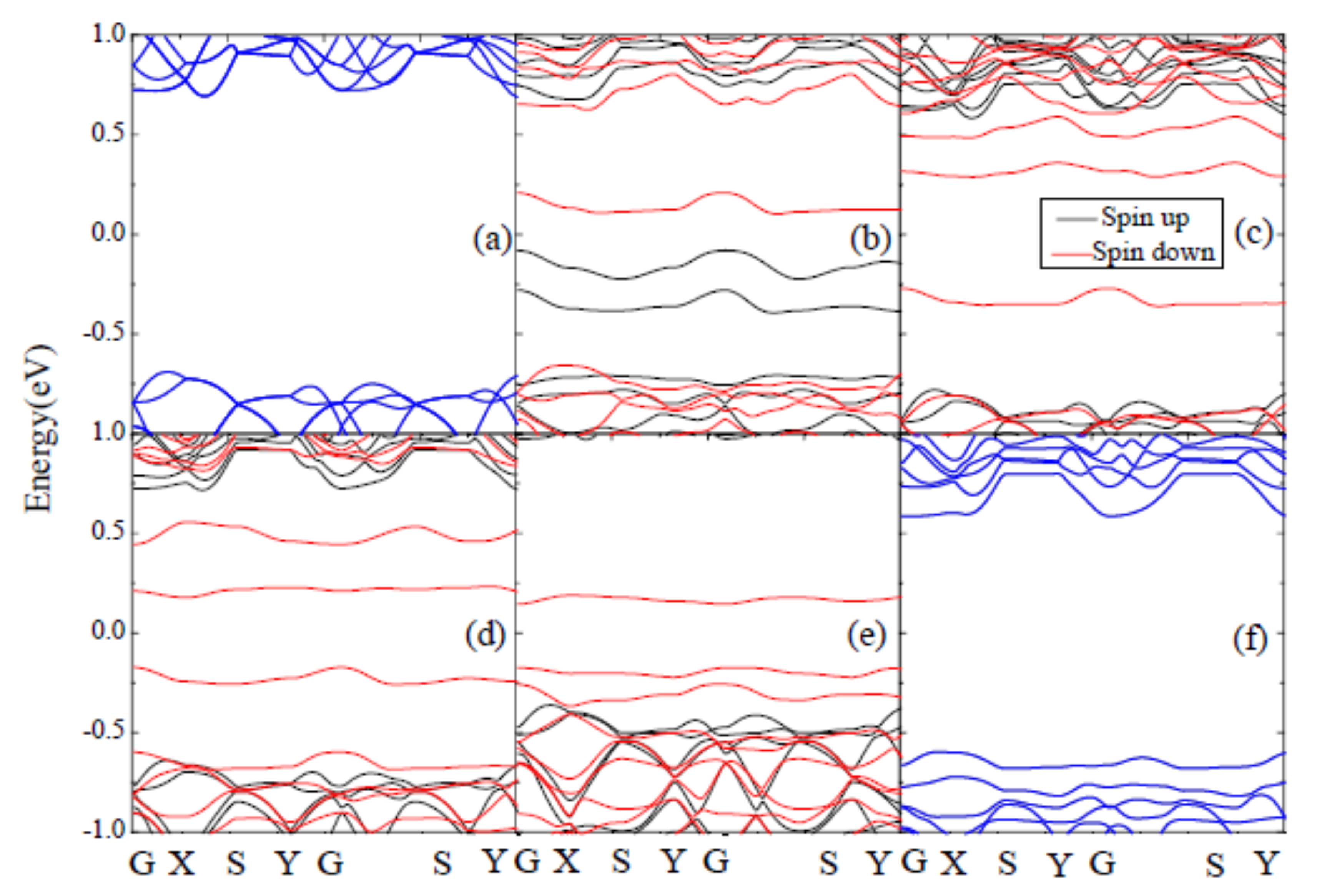
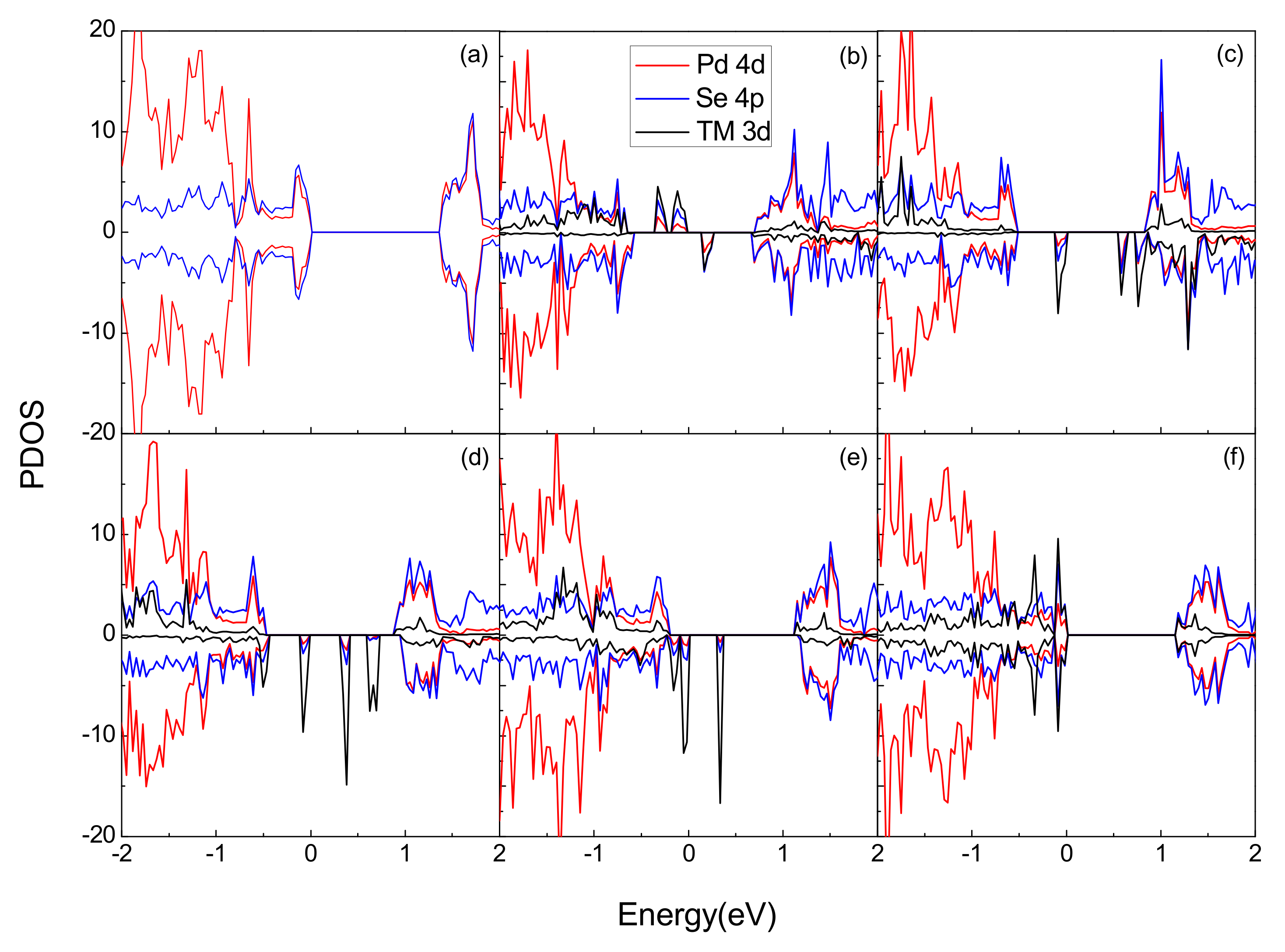
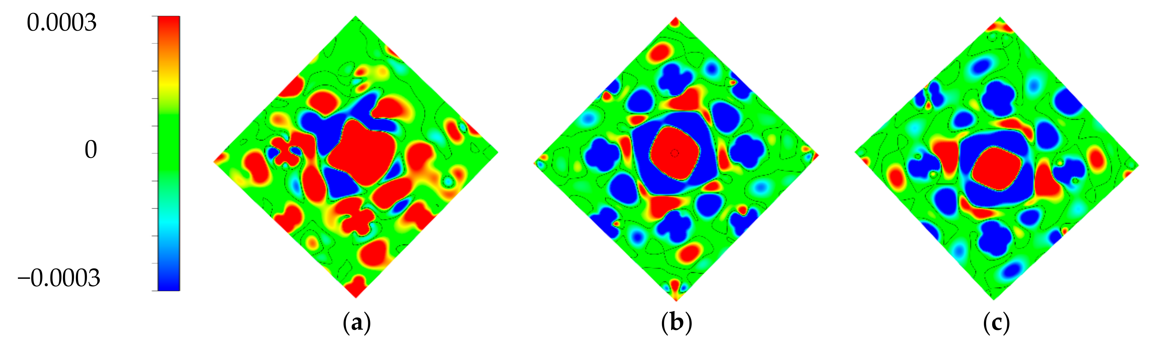
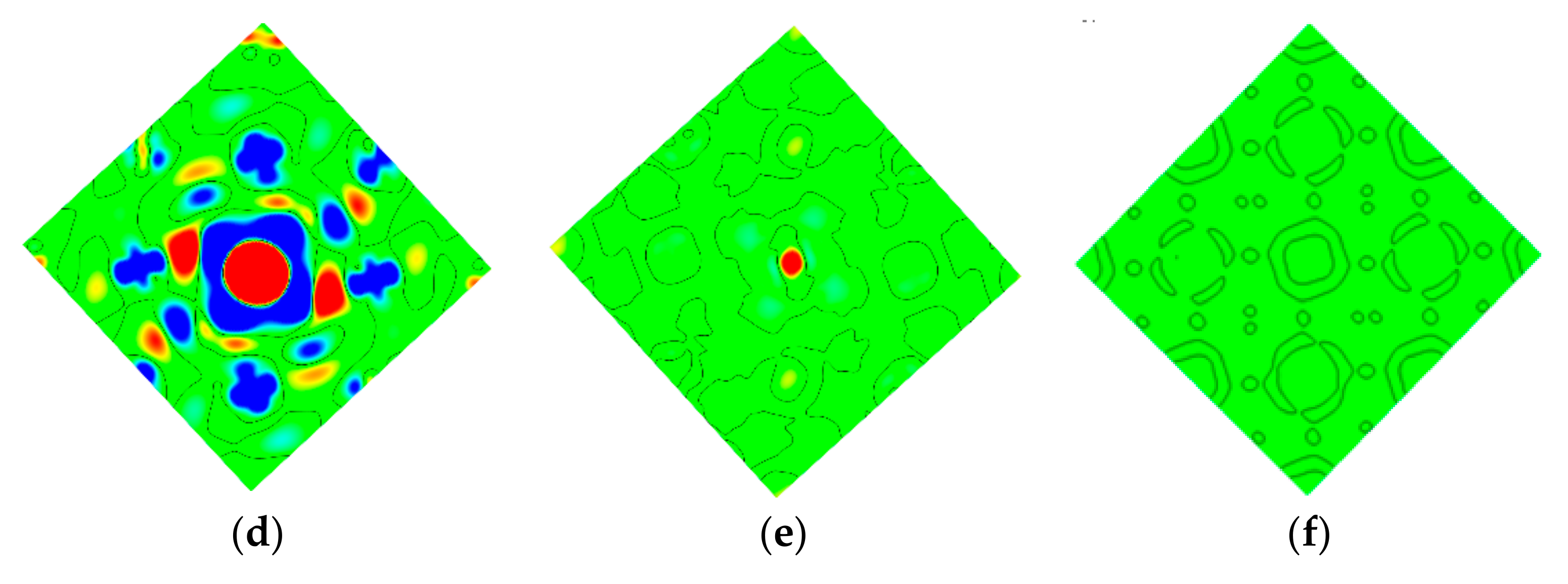
3. Results and Discussions

The fully relaxed structures are shown in Figure 1. Through comparison with the primitive cell, it can be found that the configuration of the doped system has no significant change. The changes of the bond lengths in PdSe2 before and after doping are given in Figure 2. It can be observed that the lengths of Pd-Se and Se-Se remain unchanged while the lengths of Se-dopants changed, but the changes are very subtle. These results suggest that the 3D TM atom doping has little effect on the bond lengths of PdSe2, hence, it is advisable to embed TM atoms at the dopant sites.
The spin polarization energy (Epol), which is defined as the energy difference between the nonmagnetic and ferromagnetic states (Epol = Enon − Efer), is shown in Table 1. The positive Epol means that the system favors ferromagnetism, in this case the energy of the ferromagnetic state is lower than that of the nonmagnetic state. Our calculated results are shown in Table 1, in which one finds that the system favors ferromagnetism under Cr, Mn, Fe and Co doping, however, the system with Ni dopants favors nonmagnetism due to the negative Epol.
The electronic band structures for different doped systems are depicted in Figure 3. It can be observed that the pristine PdSe2 monolayer is a semiconductor with a band gap of about 1.37 eV, which is consistent with previous experimental and theoretical results [28,29,30], however, significant changes happen after introducing the Cr, Mn, Fe and Co dopants. The band gap decreases for all systems, the value of band gaps is 1.30, 1.31, 1.32, 1.30 and 1.17 eV respectively, and there are new electronic states in the band gap. It also can be seen in Figure 3 that the band structure of pristine PdSe2 is degenerate, there is no spin polarization. For Cr-, Mn-, Fe- and Co-doped PdSe2, the band structures are nondegenerate, they show spin polarization. However, the Ni atom has little contribution to the magnetism of PdSe2. In order to make further comparisons, the magnetic moment for different doped systems are also calculated based on the Bader analysis [39], which is shown in Table 1. It can be found that the Cr-doped system has the biggest magnetic moment, about 3.71 μB, which means that the Cr doping can induce the strongest ferromagnetic coupling.
The electronic states near the Fermi level (EF) have great influence on the electron structure. Thus, it is of great importance to investigate the spin polarization properties near the EF. In Figure 4, the electronic properties for different systems are depicted by displaying the projected density of states (PDOS) with spin-up and spin-down states. The d-states of the Pd atom and p-states of the Se atom contribute most to the electronic states of pristine PdSe2 in both our calculation and previous work [28]. In fact, pristine PdSe2 is non spin polarized, while after doping the Cr, Mn, Fe and Co atoms, obvious spin asymmetry can be observed near the EF. The p-d orbital couplings between the TM atom and PdSe2 lead to the generation of the new spin states. The Cr doping system has the biggest spin-splitting, which corresponds to the strongest ferromagnetism, this result is consistent with the magnetic moment calculated in Table 1. The new electronic states for the Cr, Mn, Fe and Co doped systems near the EF are mainly originated from the 3D orbits of TM atoms. Moreover, the charge transferred from TM metals to PdSe2 will fill these new spin nondegenerate states, which lead to the systems being spin polarized. Nevertheless, there is no spin split for the Ni doping system, which means that one Ni atom doping is incapable of inducing ferromagnetism in PdSe2. Furthermore, through comparing the curves of Figure 4b–e we can find similar characteristics, this shows that the doping mechanism of the four systems are similar.
The spin density distributions of the TM doped and pristine PdSe2 systems are also given in Figure 5. The spin density is defined as Δρs = ρρ, where ρ represents the spin-up charge density, ρ is the spin-down charge density, the red and blue region in Figure 5 correspond to Δρs > 0 and Δρs < 0, respectively. It can be seen from Figure 5a–d that the system is spin polarized. Through comparing the patterns, it can be found that the area of spin density gradually decreases for the Cr-, Mn-, Fe- and Co-doped systems, however, there is almost no spin distribution for the Ni-doped and pristine system. This phenomenon is consistent with the above discussions of the PDOS and magnetic moments. Furthermore, the magnetism of PdSe2 induced by the Cr, Mn, Fe, Co and Ni atoms is gradually reduced, this is because the ability of the above TM atoms to lose electronics gradually weakens, then the amount of charge transfer gradually decreases.
To support the above results, we further analyzed the charge transfer ΔQ from the TM atoms to the PdSe2 monolayer of the four systems with the Bader analysis [39], the values of ΔQ are shown in Table 1. It is clear that the Cr-doped system has the biggest ΔQ, about 0.82 e, and the value gradually decreases for the Mn-, Fe-, Co- and Ni-doped systems, they are 0.75, 0.54, 0.37 and 0.25 e, respectively. This is because different TM atoms have different abilities to lose electrons, therefore, they have different effects on the PdSe2. We can go further and say that coulomb interactions between the different transferred charges and PdSe2 make the electronic structure change differently, hence, the varying degrees of spin polarization appear in the PdSe2 monolayer.

4. Conclusions

The electronic structure and spin polarization properties of pentagonal the PdSe2 monolayer with TM (Cr, Mn, Fe, Co and Ni) atom doping have been studied through the density functional theory. By calculating the spin polarization energy and the magnetic moment, one can see that the PdSe2 systems show different spin polarization properties and Cr-doped PdSe2 has the most stable and strongest magnetism, while the Ni doping cannot induce magnetism in PdSe2. In terms of electronic band structure, the band gap decreased after the Cr, Mn, Fe, Co and Ni atom doping, the value of band gaps is 1.30, 1.31, 1.32, 1.30 and 1.17 eV, respectively, and the branches of spin up and down is nondegenerate for the Cr, Mn, Fe, Co doped systems. The electronic properties for different systems are discussed through the PDOS, the new spin states originated from the p-d orbital couplings between the TM atoms and PdSe2. In addition, the spin density distributions and charge transfer for different PdSe2 systems also prove that the TM atom doping can induce magnetism in PdSe2 and the biggest spin polarization occurred in the Cr-doped system. Our calculations can contribute to the studies of spin polarization in pentagonal PdSe2, and the promising prospect of PdSe2 in spintronic applications.

Author Contributions

X.Z. did the calculations and wrote the paper, B.Q. collected the references, G.H. prepared the figures, W.Y. and J.R. analyzed the data, X.Y. generated the research idea. All authors read and approved the final manuscript.

Funding

The authors would like to acknowledge the financial support from the National Natural Science Foundation of China (Grant No. 11674197) and the Natural Science Foundation of Shandong Province (Grant No. ZR2018MA042). The authors thank the Taishan Scholar Project of Shandong Province for its support.

Conflicts of Interest

The authors declare no conflict of interest.

References

  1. Novoselov, K.S.; Geim, A.K.; Morozov, S.V.; Jiang, D.A.; Zhang, Y.; Dubonos, S.V.; Grigorieva, I.V.; Firsov, A.A. Electric field effect in atomically thin carbon films. Science 2004, 306, 666–669. [Google Scholar] [CrossRef] [PubMed]
  2. Zhang, Y.; Small, J.P.; Amori, M.E.; Kim, P. Electric field modulation of galvanomagnetic properties of mesoscopic graphite. Phys. Rev. Lett. 2005, 94, 176803. [Google Scholar] [CrossRef] [PubMed]
  3. Stankovich, S.; Dikin, D.A.; Dommett, G.H.; Kohlhaas, K.M.; Zimney, E.J.; Stach, E.A.; Piner, R.D.; Nguyen, S.T.; Ruoff, R.S. Graphene-based composite materials. Nature 2006, 442, 282. [Google Scholar] [CrossRef] [PubMed]
  4. Xu, S.C.; Man, B.Y.; Jiang, S.Z.; Chen, C.S.; Yang, C.; Liu, M.; Huang, Q.J.; Zhang, C.; Bi, D.; Meng, X.; et al. Watt-level passively Q-switched mode-locked YVO4/Nd:YVO4 laser operating a 1.06 μm using graphene as a saturable absorber. Opt. Laser. Technol. 2014, 56, 393–397. [Google Scholar] [CrossRef]
  5. Zhu, H.; Zhao, L.; Liu, J.; Xu, S.; Cai, W.; Jiang, S.; Zheng, L.; Su, L.; Xu, J. Monolayer graphene saturable absorber with sandwich structure for ultrafast solid-state laser. Opt. Laser. Technol. 2015, 55, 081304. [Google Scholar] [CrossRef]
  6. Warner, J.H.; Rummeli, M.H.; Bachmatiuk, A.; Büchner, B. Atomic resolution imaging and topography of boron nitride sheets produced by chemical exfoliation. ACS Nano 2010, 4, 1299–1304. [Google Scholar] [CrossRef] [PubMed]
  7. Li, L.; Yu, Y.; Ye, G.J.; Ge, Q.; Ou, X.; Wu, H.; Feng, D.; Chen, X.H.; Zhang, Y. Black phosphorous field-effect transistors. Nat. Nanotechnol. 2014, 9, 372. [Google Scholar] [CrossRef] [PubMed]
  8. Jariwala, D.; Sangwan, V.K.; Lauhon, L.J.; Marks, T.J.; Hersam, M.C. Emerging device applications for semiconducting two-dimensional transition metal dichalcogenides. ACS Nano 2014, 8, 1102–1120. [Google Scholar] [CrossRef] [PubMed]
  9. Miró, P.; Audiffred, M.; Heine, T. An atlas of two-dimensional materials. Chem. Soc. Rev. 2014, 43, 6537–6554. [Google Scholar] [CrossRef] [PubMed]
  10. Mark, K.F.; McGill, K.L.; Park, J.; McEuen, P.L. The valley Hall effect in MoS2 transistors. Science 2014, 344, 1489–1492. [Google Scholar]
  11. Ahmed, S.; Ding, X.; Bao, N.; Bian, P.; Zheng, R.; Wang, Y.; Murmu, P.P.; Kennedy, J.V.; Liu, R.; Fan, H.; et al. Inducing high coercivity in MoS2 nanosheets by transition element doping. Chem. Mater. 2017, 29, 9066–9074. [Google Scholar] [CrossRef]
  12. Deng, S.; Zhong, Y.; Zeng, Y.; Wang, Y.; Yao, Z.; Yang, F.; Lin, S.; Wang, X.; Lu, X.; Xia, X.; et al. Directional construction of vertical nitrogen-doped 1T-2H MoSe2/graphene shell/core nanoflake arrays for efficient hydrogen evolution reaction. Adv. Mater. 2017, 29, 1700748. [Google Scholar] [CrossRef] [PubMed]
  13. Chen, Y.; Gan, L.; Li, H.; Ma, Y.; Zhai, T. Achieving uniform monolayer transition metal dichalcogenides film on silicon wafer via silanization treatment: A typical study on WS2. Adv. Mater. 2017, 29, 1603550. [Google Scholar] [CrossRef] [PubMed]
  14. Fan, Z.Q.; Xie, F.; Jiang, X.W.; Wei, Z.; Li, S.S. Giant decreasing of spin current in a single molecular junction with twisted zigzag graphene nanoribbon electrodes. Carbon 2016, 110, 200–206. [Google Scholar] [CrossRef]
  15. Yan, W.; Txoperena, O.; Llopis, R.; Dery, H.; Hueso, L.E.; Casanova, F. Casanova1, A two-dimensional spin field-effect switch. Nat. Commun. 2016, 7, 13372. [Google Scholar] [CrossRef] [PubMed]
  16. Zhang, Z.; Zou, X.; Crespi, V.H.; Yakobson, B.I. Intrinsic magnetism of grain boundaries in two-dimensional metal dichalcogenides. ACS Nano 2013, 7, 10475–10481. [Google Scholar] [CrossRef] [PubMed]
  17. Guan, J.; Yu, G.; Ding, X.; Chen, W.; Shi, Z.; Huang, X.; Sun, C. The effects of the formation of stone-wales defects on the electronic and magnetic properties of silicon carbide nanoribbons: A first-principles investigation. Chem. Phys. Chem. 2013, 14, 2841–2852. [Google Scholar] [CrossRef] [PubMed]
  18. Barone, V.; Peralta, J.E. Magnetic boron nitride nanoribbons with tunable electronic properties. Nano. Lett. 2008, 8, 2210–2214. [Google Scholar] [CrossRef] [PubMed]
  19. Gao, G.; Ding, G.; Li, J.; Yao, K.; Wu, M.; Qian, M. Monolayer MXenes: promising half-metals and spin gapless semiconductors. Nanoscale 2016, 8, 8986–8994. [Google Scholar] [CrossRef] [PubMed] [Green Version]
  20. Hashmi, A.; Hong, J. Transition metal doped phosphorene: first-principles study. J. Phys. Chem. C 2015, 119, 9198–9204. [Google Scholar] [CrossRef]
  21. Yang, Y.; Guo, M.; Zhang, G.; Li, W. Tuning the electronic and magnetic properties of porous graphene like carbon nitride through 3d transition-metal doping. Carbon 2017, 117, 120–125. [Google Scholar] [CrossRef]
  22. Chen, Q.; Ouyang, Y.; Yuan, S.; Li, R.; Wang, J. Uniformly wetting deposition of Co atoms on MoS2 monolayer: A promising two-dimensional robust half-metallic ferromagnet. ACS Appl. Mater. Interfaces 2014, 6, 16835–16840. [Google Scholar] [CrossRef] [PubMed]
  23. Kan, E.J.; Xiang, H.J.; Wu, F.; Tian, C.; Lee, C.; Yang, J.L.; Whangbo, M.H. Prediction for room-temperature half-metallic ferromagnetism in the half-fluorinated single layers of BN and ZnO. Appl. Phys. Lett. 2010, 9, 122503. [Google Scholar] [CrossRef]
  24. Yuan, X.B.; Yang, M.S.; Tian, Y.L.; Cai, L.L.; Ren, J.F. Spin polarization properties of thiophene molecule adsorbed to the edge of zigzag graphene nanoribbon. Synthetic Met. 2017, 226, 46–49. [Google Scholar] [CrossRef]
  25. Yuan, X.B.; Tian, Y.L.; Zhao, X.W.; Yue, W.W.; Hu, G.C.; Ren, J.F. Spin polarization properties of benzene/graphene with transition metals as dopants: First principles calculations. Appl. Surf. Sci. 2018, 439, 1158–1162. [Google Scholar] [CrossRef]
  26. Ahmad, S. Strain dependent tuning electronic properties of noble metal dichalcogenides PdX2 (x = s, se) monolayer. Mater. Chem. Phys. 2017, 198, 162–166. [Google Scholar] [CrossRef]
  27. Chow, W.L.; Yu, P.; Liu, F.; Hong, J.; Wang, X.; Zeng, Q.; Hsu, C.H.; Zhu, C.; Zhou, J.; Wang, X.; et al. High mobility 2d palladium diselenide field-effect transistors with tunable ambipolar characteristics. Adv. Mater. 2017, 29, 14090–14097. [Google Scholar] [CrossRef] [PubMed]
  28. Sun, J.; Shi, H.; Siegrist, T.; Singh, D.J. Electronic, transport, and optical properties of bulk and mono-layer PdSe2. Appl. Phys. Lett. 2015, 107, 153902. [Google Scholar] [CrossRef]
  29. Oyedele, A.D.; Yang, S.; Liang, L.; Puretzky, A.A.; Wang, K.; Zhang, J.; Yu, P.; Pudasaini, P.R.; Ghosh, A.W.; Liu, Z.; et al. PdSe2: pentagonal two-dimensional layers with high air stability for electronics. J. Am. Chem. Soc. 2017, 139, 14090–14097. [Google Scholar] [CrossRef] [PubMed]
  30. Puretzky, A.A.; Oyedele, A.D.; Xiao, K.; Haglund, A.V.; Sumpter, B.G.; Mandrus, D.; Geohegan, D.B.; Liang, L. Anomalous interlayer vibrations in strongly coupled layered PdSe2. 2D Mater. 2018, 5, 035016. [Google Scholar] [CrossRef]
  31. Nguyen, G.D.; Liang, L.; Zou, Q.; Fu, M.; Oyedele, A.D.; Sumpter, B.G.; Liu, Z.; Gai, Z.; Xiao, K.; Li, A.P. 3D Imaging and Manipulation of Subsurface Selenium Vacancies in PdSe2. Phys. Rev. Lett. 2018, 121, 086101. [Google Scholar] [CrossRef] [PubMed]
  32. Quhe, R.; Fei, R.; Liu, Q.; Zheng, J.; Li, H.; Xu, C.; Ni, Z.; Wang, Y.; Yu, D.; Gao, Z.; et al. Tunable and sizable band gap in silicene by surface adsorption. Sci. Rep. 2012, 2, 853. [Google Scholar] [CrossRef] [PubMed]
  33. Zhang, S.H.; Liu, B.G. Hole-doping-induced half-metallic ferromagnetism in highly-air-stable PdSe2 monolayer under uniaxial stress. J. Mater. Chem. C 2018, 6, 6792–6798. [Google Scholar] [CrossRef]
  34. Kresse, G.; Furthmüller, J. Efficient iterative schemes for ab initio total-energy calculations using a plane-wave basis set. Phys. Rev. B 1996, 54, 11169. [Google Scholar] [CrossRef]
  35. Kresse, G.; Joubert, D. From ultrasoft pseudopotentials to the projector augmented-wave method. Phys. Rev. B 1999, 59, 1758–1775. [Google Scholar] [CrossRef]
  36. Dos Santos, R.B.; Rivelino, R.; de Brito Mota, F.; Gueorguiev, G.K. Effects of N doping on the electronic properties of a small carbon atomic chain with distinct sp2 terminations: A first-principles study. Phys. Rev. B 2011, 84, 075417. [Google Scholar] [CrossRef]
  37. Freitas, R.R.; de Brito Mota, F.; Rivelino, R.; De Castilho, C.M.C.; Kakanakova-Georgieva, A.; Gueorguiev, G.K. Spin-orbit-induced gap modification in buckled honeycomb XBi and XBi3 (X = B, Al, Ga, and In) sheets. J. Phys. Condens. Matter 2015, 27, 485306. [Google Scholar] [CrossRef] [PubMed]
  38. Cai, L.; Tian, Y.; Yuan, X.; Hu, G.; Ren, J. Electronic structures of spinterface for thiophene molecule adsorbed at Co, Fe, and Ni electrode: First principles calculations. Appl. Surf. Sci. 2016, 389, 916–920. [Google Scholar] [CrossRef]
  39. Tang, W.; Sanville, E.; Henkelman, G. A grid-based bader analysis algorithm without lattice bias. J. Phys. Condens. Matter 2009, 21, 084204. [Google Scholar] [CrossRef] [PubMed]
Figure 1. Top (a) and side (b) views of PdSe2 configuration. Green, purple and yellow balls represent Se, Pd, and dopant (Cr, Mn, Fe, Co and Ni atoms) respectively.
Materials 11 02339 g001
Figure 2. Bond length for different PdSe2 systems.
Materials 11 02339 g002
Figure 3. Electronic band structures of different doped systems, (a) pristine system, (b) Cr-doped system, (c) Mn-doped system, (d) Fe-doped system, (e) Co-doped system, (f) Ni-doped system, respectively.
Materials 11 02339 g003
Figure 4. Projected density of states (PDOS) of the different doped systems, (a) pristine system, (b) Cr-doped system, (c) Mn-doped system, (d) Fe-doped system, (e) Co-doped system, (f) Ni-doped system, respectively.
Materials 11 02339 g004
Figure 5. Spin density distributions for different doped systems. (af) correspond to Cr-, Mn-, Fe-, Co-, Ni- doped and pristine PdSe2, respectively. The 2D planes are determined by two Pd atoms and the dopants for the doped system, three Pd atoms for pristine PdSe2.
Materials 11 02339 g005aMaterials 11 02339 g005b
Table 1. Calculated spin polarization energy, charge transfer and magnetic moments of PdSe2 with different dopants.
SystemCr-DopedMn-DopedFe-DopedCo-DopedNi-DopedPristine PdSe2
Epol (eV)2.781.610.820.21−1.25-
ΔQ (e)0.820.750.540.370.25-
Magnetic Moment (μB)3.712.991.991.000.000.00

