Article

Advances in Thin-Film Si Solar Cells by Means of SiOx Alloys

Italian National Agency for New Technologies, Energy and Sustainable Economic Development (ENEA), Portici Research Center, P.le E. Fermi 1, Portici 80055, Italy
*
Author to whom correspondence should be addressed.
Energies 2016, 9(3), 218; https://doi.org/10.3390/en9030218
Submission received: 14 January 2016 / Revised: 4 March 2016 / Accepted: 10 March 2016 / Published: 18 March 2016
(This article belongs to the Special Issue Key Developments in Thin Film Solar Cells)

Abstract

:
The conversion efficiency of thin-film silicon solar cells needs to be improved to be competitive with respect to other technologies. For a more efficient use of light across the solar spectrum, multi-junction architectures are being considered. Light-management considerations are also crucial in order to maximize light absorption in the active regions with a minimum of parasitic optical losses in the supportive layers. Intrinsic and doped silicon oxide alloys can be advantageously applied within thin-film Si solar cells for these purposes. Intrinsic a-SiOx:H films have been fabricated and characterized as a promising wide gap absorber for application in triple-junction solar cells. Single-junction test devices with open circuit voltage up to 950 mV and ~1 V have been demonstrated, in case of rough and flat front electrodes, respectively. Doped silicon oxide alloys with mixed-phase structure have been developed, characterized by considerably lower absorption and refractive index with respect to standard Si-based films, accompanied by electrical conductivity above 10−5 S/cm. These layers have been successfully applied both into single-junction and micromorph tandem solar cells as superior doped layers with additional functionalities.

1. Introduction

The thin-film silicon solar cell technology is based on a versatile set of materials and alloys, in both amorphous and microcrystalline form, grown from precursor gases by means of a capacitively coupled plasma. It is a mature and reliable photovoltaic technology with the advantages of large-area, low-cost of manufacturing, abundance of raw materials, and aesthetics of products. However, the conversion efficiency needs to be improved to be competitive with respect to other technologies. A special attention to light management within the device and the exploitation of multi-junction architectures are the main aspects under exploration to increase the efficiency. Since the technology relies on thin-films of a weakly absorbing material, the application of light-management concepts is crucial in order to maximize light absorption in the active regions with a minimum of parasitic optical losses in the supportive layers. Various strategies are being investigated, going from improved light scattering textures to advanced schemes based on nanopillars or plasmonics, accompanied by material research toward reduced parasitic losses [1]. In addition, for a more efficient use of light across the solar spectrum, multi-junction architectures have to be considered, by stacking thin component cells dedicated to the absorption of specific portions of the spectrum. Within the thin-film Si technology the highest efficiencies are indeed obtained with multi-junction devices, already starting with the very promising micromorph (amorphous silicon/microcrystalline silicon—a-Si:H/µc-SiH) tandem combination, for which a confirmed record efficiency of 12.3% has been demonstrated on large area modules (1.4 m2) [2].
The highest conversion efficiencies have so far been obtained with triple-junction cells: 16.3% initial, shown by United Solar with the a-Si:H/a-SiGe:H/μc-Si:H combination [3], and 13.6% stable, demonstrated by the AIST group with the a-Si:H/µc-Si:H/µc-Si:H configuration [4]. In these cases, a-Si:H is used as top cell absorber. However, theoretical analysis suggests that the highest efficiency for a triple junction can be actually obtained when the bandgap of the top cell absorber is around 2.0 eV, owing to the increase in open circuit voltage (VOC) [5]. The development of wide bandgap Si-based absorber materials is then a crucial factor for exploiting the efficiency potential of multi-junction solar cells. In this context, hydrogenated amorphous silicon oxide (a-SiOx:H) appears to be a promising candidate, since its energy gap can be significantly widened by adjusting the oxygen content [6,7,8]. Silicon oxide alloys can be useful also as more transparent inactive layers, thus helping to reduce the parasitic light absorption. In this case mixed-phase nanocrystalline doped silicon oxide (nc-SiOx:H) is demonstrating interesting capabilities, and various versions are now being successfully used as superior doped layers and/or reflecting layers in multi-junction thin-film Si solar cells [3,9,10,11,12,13,14].
In the present work, recent progress is reported based on the use of suitably adapted silicon oxide alloys within p-i-n type thin-film Si solar cells. The development of a promising wide gap a-SiOx:H absorber for application in triple-junction cells is firstly presented. The material is grown by plasma enhanced chemical vapor deposition (PECVD) in the very high frequency (VHF) regime. Since the incorporation of oxygen easily generates defects, different deposition conditions have been investigated in order to optimize both optical and electrical properties. Afterwards, the development of doped nc-SiOx:H films as advanced supportive layers is reported, showing that improved light management is feasible while keeping a simple cell design. In particular, our investigation of n-type doped nanostructured silicon oxide as dual-function layer both at intermediate and backside position in micromorph tandem cells is presented, accompanied by a description of the structural and electro-optical properties of the material used in the devices. The characterization of p-type doped nc-SiOx:H films and the application of the material as advanced window layer is finally shown.

2. Results

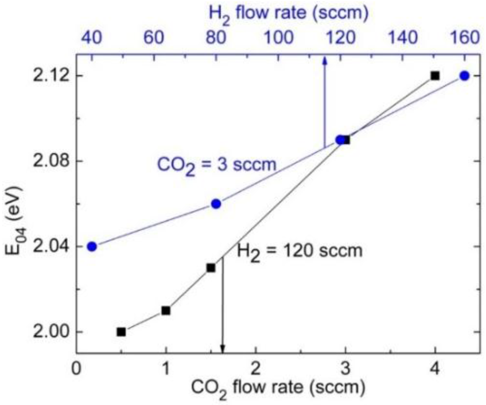
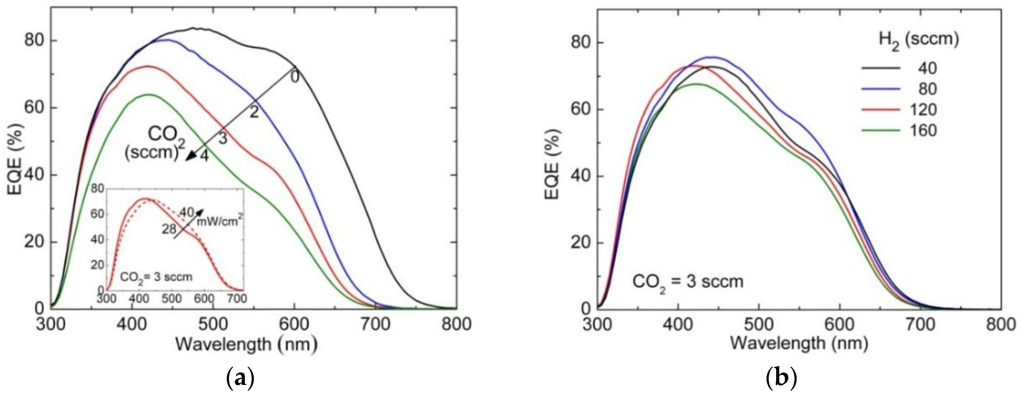
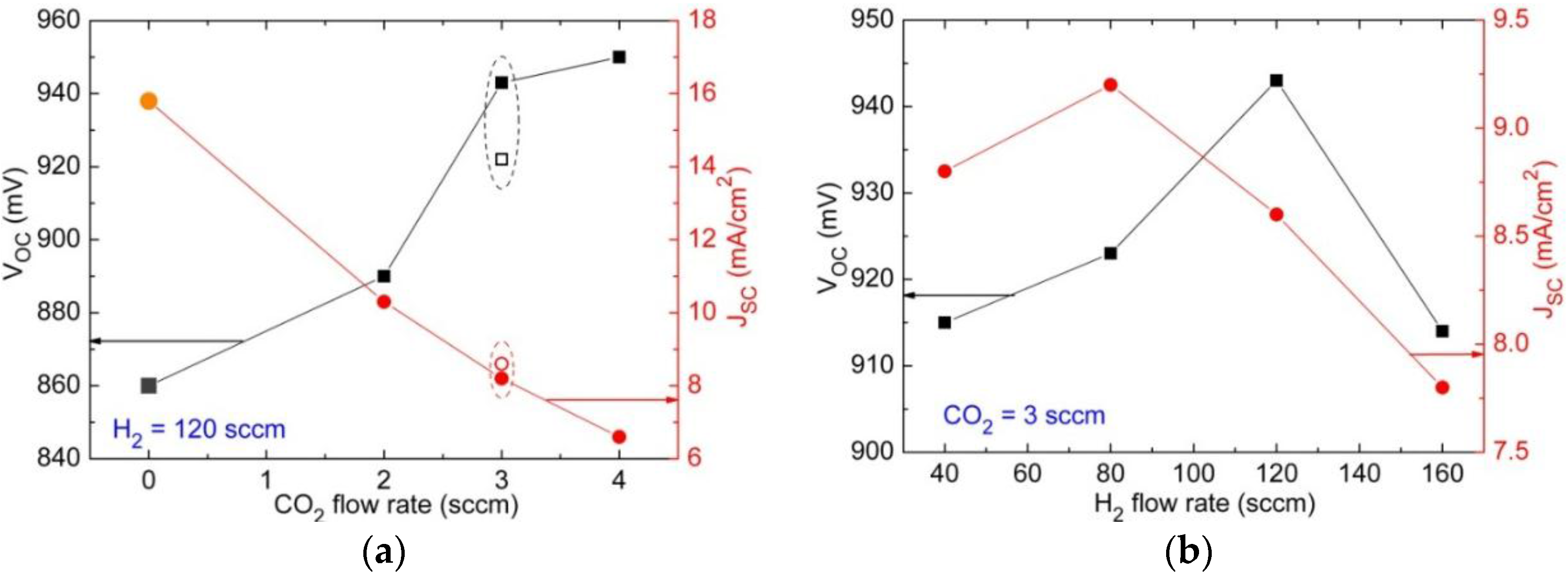
2.1. a-SiOx:H as Wide Bandgap Absorber

The a-SiOx:H films were grown by VHF-PECVD using silane (SiH4) and carbon dioxide (CO2) as Si and O sources, respectively. Rather high flow rate of hydrogen (H2) was also included in the gas mixture in order to reduce the defect density in the material, which increases with oxygen concentration [6]. The H2 dilution has to be carefully controlled to obtain device-quality a-SiOx:H with a wide bandgap. In fact, too high hydrogen dilution can cause the phase transition from amorphous to microcrystalline silicon oxide. This is a mixed-phase material consisting of a-SiOx:H and microcrystalline silicon (µc-Si:H) phases, where the latter component determines the material bandgap. While varying the hydrogen dilution, the possible presence of ordered phase has been thus checked through Raman analysis.
A drawback of the high H2 dilution is the low deposition rate, which remains in the range 0.7–1.1 Å/s against ~2 Å/s for standard a-Si:H deposited in the same process chamber. The large H2 dilution on the other hand also contributes to the desired increase of the material bandgap. The evolution of the bandgap, parametrized by the energy E04 at which the absorption coefficient reaches 104 cm−1, as a function of CO2 flow rate (at H2 = 120 sccm) and of H2 flow rate (at CO2 = 3 sccm) is shown in Figure 1. In both the cases, an increase of the bandgap is obtained. However, considering the range of values investigated for the two parameters (CO2 and H2), as expected oxygen acts more effectively than hydrogen on the optical properties of the films. E04 up to 2.12 eV has been measured, that is well above the value of our standard a-Si:H (1.9 eV). The electrical properties of the samples have been investigated by measuring the lateral conductivity in the dark (σD) and under illumination (σL). The σD values are in the range 10−10–10−11 S/cm and the photoresponse ratio (σLD) is ~103–104. A decrease of σL with increasing CO2 flow rate, and consequently of oxygen content in the film, has been observed. This can be attributed to the bandgap widening that causes a reduction of the photogenerated carrier density. However, since σL is proportional to the mobility-lifetime product of the generated carriers, its reduction could be also ascribed to an enhanced content of defects acting as recombination sites, caused by the incorporation of oxygen atoms [6].
The potentiality of the material as absorber layer has been tested within thin p-i-n single junction solar cells (150-nm-thick i-layer), grown on commercial Asahi-VU glass substrates coated with textured transparent conducting oxide (TCO). A solar cell with a-Si:H absorber layer with the same thickness and identical doped and contact layers has been used as reference cell.
The bandgap variation with oxygen incorporation in the absorber material is evident in the spectral response of the devices. Figure 2 shows the external quantum efficiency (EQE) of a solar cell series with intrinsic layer grown with CO2 flow rates ranging from 2 sccm to 4 sccm, H2 flow rate fixed at 120 sccm and discharge power density of 28 mW/cm2. In the same figure the EQE of the reference cell with standard a-Si:H absorber layer is also reported (black line). The corresponding short circuit current densities (JSC) are reported in Figure 3a (right axis). The increase of the bandgap with oxygen addition leads to a decrease of the EQE, and consequently of JSC, due to the missing absorption of the low-energy photons. The JSC goes from 15.8 mA/cm2, measured on the reference cell, to 6.6 mA/cm2 obtained at the highest CO2 value used in this study. The inset to Figure 2a shows in addition the effect of the discharge power density increased from 28 mW/cm2 (solid line) to 40 mW/cm2 (dashed line) for CO2 = 3 sccm. The short circuit current increases from 8.2 to 8.6 mA/cm2 (open circle in Figure 3a), due to the slightly improved response in the 450–600 nm wavelength range. On the other side, at 28 mW/cm2 an EQE enlargement is observed at lower wavelengths. This is likely due to the softened ion bombardment at the p-i interface when the power is reduced, which determines a better quality of this interface.
The effect of hydrogen dilution on the spectral response is shown in Figure 2b for a cell series with absorber layer grown with CO2 flow rate of 3 sccm and different H2 flow rates in the range 40–160 sccm. The corresponding JSCs are reported in Figure 3b (right axis). An initial increase of the EQE is observed, when H2 goes from 40 sccm to 80 sccm, and an increase of JSC from 8.8 mA/cm2 to 9.2 mA/cm2 is registered. Since the a-SiOx:H bandgap increases with the hydrogen dilution (Figure 1), this EQE enlargement is not related to bandgap variation but is likely due to better material quality when the hydrogen dilution increases. A further increase of the H2 flow rate on the other hand determines a reduction of the EQE, particularly for the largest value (160 sccm) where a JSC of 7.8 mA/cm2 is evaluated. The JSC reduction for H2 > 80 sccm is mainly due to the enlargement of the bandgap, although also other material properties could play a role.
As for the overall photovoltaic performance, the J-V characteristics under AM1.5 illumination have shown rather poor fill factors (FF), in the range 47%–50%, as opposed to values around 70% measured for the reference a-Si:H cell. Because of the limited Jsc and FF values, globally the conversion efficiency stays below 5%, versus 9.3% measured for the reference cell. The low FF is caused by large series resistance values (RS), which are two or three times higher than the RS measured for the baseline cell. The increased RS could be due to the properties of the doped layers, developed for our standard a-Si:H cells, likely not appropriate for the high bandgap materials under test. Also the quality of the absorber layer could contribute to the observed FF drop. Figure 3 (left axes) shows the evolution of the open circuit voltage (VOC) for the two cell series in Figure 2. As for the series deposited with different CO2 values (Figure 3a), starting from the value measured on the standard a-Si:H cell (860 mV), we observe a VOC increase, due to the enlargement of the absorber bandgap, up to 950 mV obtained for CO2 = 4 sccm. At CO2 = 3 sccm, a drop of VOC from 943 mV to 915 mV is observed when the discharge power density is increased from 28 mW/cm2 to 40 mW/cm2 (open square in the figure). It is well known that the open circuit voltage is influenced by the defect density at the interfaces that determines additional recombination. This is particularly true for the interface which is deposited first, here the p-i interface [15]. The VOC value and the EQE behavior (inset to Figure 2a) at short wavelengths obtained using CO2 = 3 sccm and plasma power density of 28 mW/cm2 thus seem to suggest that this growth regime favors a better quality of the p-i interface. Figure 3b shows the VOC evolution for the series with variable H2 dilution. The VOC increases for H2 flow rate up to 120 sccm, as an effect of the enlargement of the a-SiOx:H bandgap, and then decreases again. The presence of porous zones in the absorber material [16] and/or the proximity of the transition region between amorphous and microcrystalline structure [6] can explain the VOC drop when high H2 values are used.
The use of 3 sccm and 120 sccm of CO2 and H2, respectively, plus a discharge power density of 28 mW/cm2, has been finally identified as the most favorable deposition condition within this study. A ~10% increase of VOC has been achieved with respect to the reference a-Si:H cell, when using commercial rough substrates. For triple junction solar cells, where lower currents have to be collected, smoother substrates are, in principle, feasible. In this case even larger ΔVOC is expected as an effect of the improved material quality, less prone to formation of porous defective zones. The potential ΔVOC for the triple-junction application has been estimated by testing the selected a-SiOx:H material in a solar cell grown on in-house flat front electrode (sputtered ZnO:Al on glass). The J-V characteristic under solar simulator is reported in Figure 4 (red line). With absence of light scattering the photocurrent is reduced with respect to the same cell on rough substrate (black line). In addition the FF is inferior, mostly due to the non-optimized electrical properties of the sputtered ZnO:Al used as front electrode. The VOC increase is however remarkable, with a measured value of ~1 V.

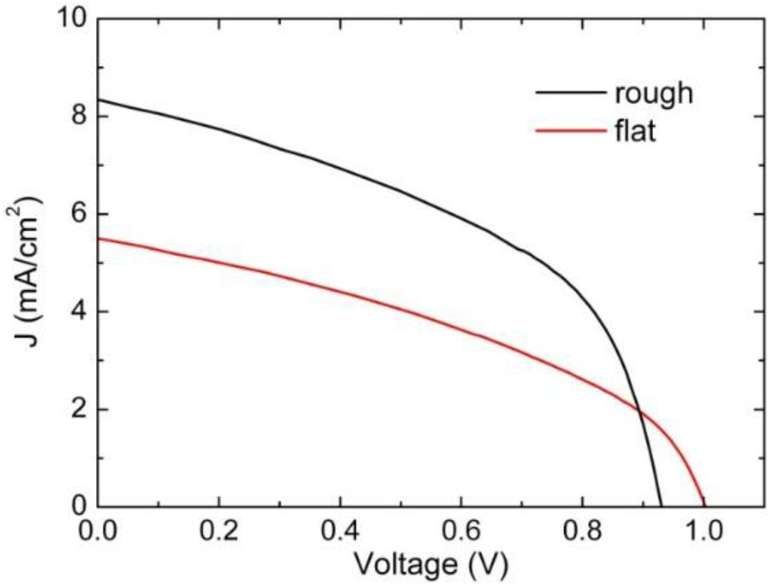
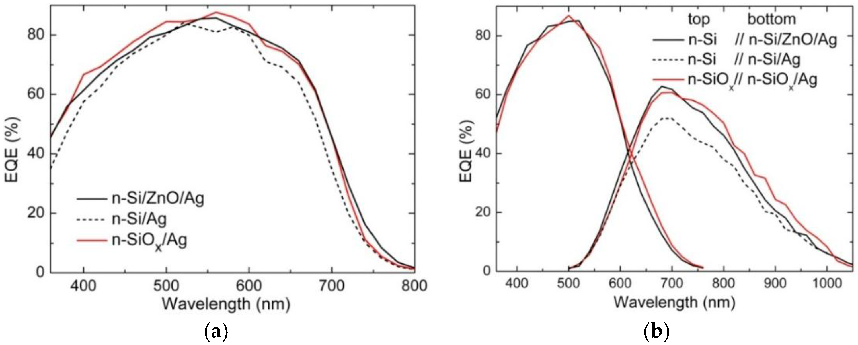
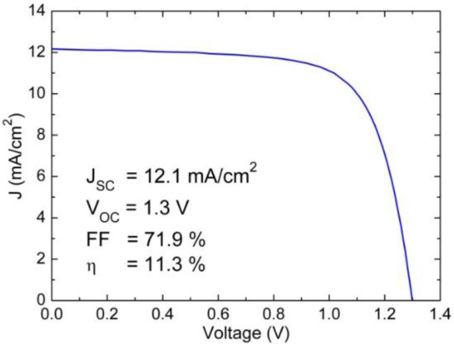
2.2. Doped Mixed-Phase nc-SiOx:H for Improved Light Management

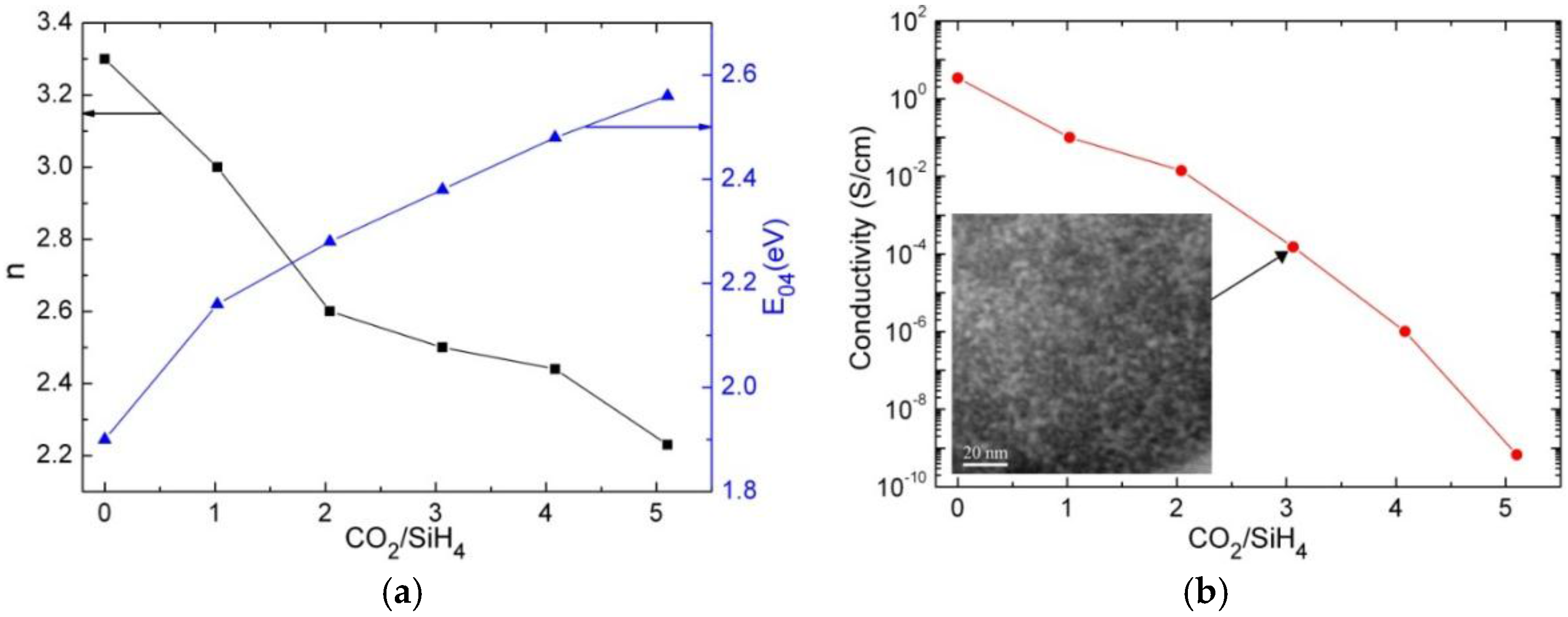
2.2.1. n-Type Material (n-SiOx)

Phosphorus-doped nc-SiOx:H films (n-SiOx) were grown by PECVD using a mixture of SiH4, CO2, H2, and phosphine (PH3) as doping gas. Different oxygen content can be easily obtained in the layers by varying the CO2/SiH4 flow rate ratio with consequent modification of structural, optical, and electrical properties. The addition of oxygen in the material interferes with the crystalline growth. A large H2 dilution was thus applied to favor the formation of a mixed phase, with Si nanocrystals in an amorphous matrix containing oxygen, thanks to a growth mechanism like the surface diffusion model proposed for microcrystalline silicon [17]. The mixed phase structure is desired here because the larger doping efficiency of crystalline versus amorphous material allows for enhanced conductivity with respect to amorphous alloys (thanks to the Si nanocrystal component), while keeping significant margins for adjustment of the optical constants with incorporation of oxygen in the amorphous matrix. Figure 5a shows the variation of refractive index (n) and bandgap (E04) when the CO2/SiH4 flow rate ratio is changed in the range 0–5: n decreases down to 2.2 and E04 simultaneously increases up to ~2.6 eV, while the material becomes more transparent. The conductivity (Figure 5b) decreases of several orders, from a few S/cm down to the range of 10−10 S/cm with the increase of the amorphous phase content, where the doping is less efficient. Favorable doped layers for thin-film Si solar cells are thus obtained at intermediate values of the CO2/SiH4 ratio, thanks to the refractive index already well below the value for microcrystalline Si (~2.5 vs. 3.5 at 600 nm) accompanied by still practical electrical conductivity values (above 10−5 S/cm). The pronounced phase separation at nanometer scale of these layers, which promotes the appropriate electrical properties, is shown in Figure 5b.
Showing a good compromise between low-n/increased-transparency on one side and reasonable electrical conductivity on the other, this material can be used as advanced substitute of the n-layer in thin-film silicon solar cells with the advantage of a better light management. The use of an n-type layer that (1) is more transparent and (2) has lower refractive index with respect to the standard n-layer allows both to reduce the parasitic absorption losses within the layer and to give additional functionalities to the layer. Figure 6 shows the advances that can be achieved with application of n-SiOx for both the single-junction (a) and the micromorph tandem design (b). For the latter case, the n-layer of both the top and bottom cell can be replaced with beneficial effects. For single p-i-n a-Si:H solar cells (a) and for the bottom junction of micromorph devices (b), the n-SiOx layer allows simplification of the back reflecting contact by functioning also as appropriate low-n spacer between the Si layer stack and the metal, in place of the ZnO buffer usually included in the cell design to reduce the plasmonic losses [18]. The major role played by the ZnO layer is illustrated in Figure 6a,b for the cells with standard Si based n-layer (black lines: solid and dashed for the cells with and without ZnO, respectively). When substituting the standard Si-based n-layer with the SiOx-based material, the ZnO layer is not necessary anymore. The comparison of a-Si:H single junction cells with n-Si/ZnO/Ag and n-SiOx/Ag back configurations shows indeed similar spectral responses (Figure 6a). With the enlargement of the usable spectral range when a μc-Si:H absorber is included, as in the case of the bottom cell of the tandem devices, an even superior EQE with respect to the standard configuration is obtained with use of n-SiOx/Ag (Figure 6b). With this application, the ZnO deposition step at the back contact realization stage can be eliminated, preserving the same (for a-Si:H solar cells) or achieving an even larger (for micromorph solar cells) spectral response, with a clear advantage at production level. In the tandem configuration, the n-SiOx layer applied in the top cell can function also as intermediate reflector, as shown by the enlargement of the top cell EQE (Figure 6b). This is achieved without the need of a dedicated additional low-n layer, with the advantage of avoiding the introduction of further parasitic optical losses affecting the spectral response of the bottom cell. This application allows for a reduction of the top a-Si:H absorber thickness, with advantages for the stabilized cell efficiency. Finally, Figure 7 shows the J-V curve under solar simulator of a micromorph tandem cell with simplified architecture (no ZnO buffer) implementing the developed n-SiOx layer.

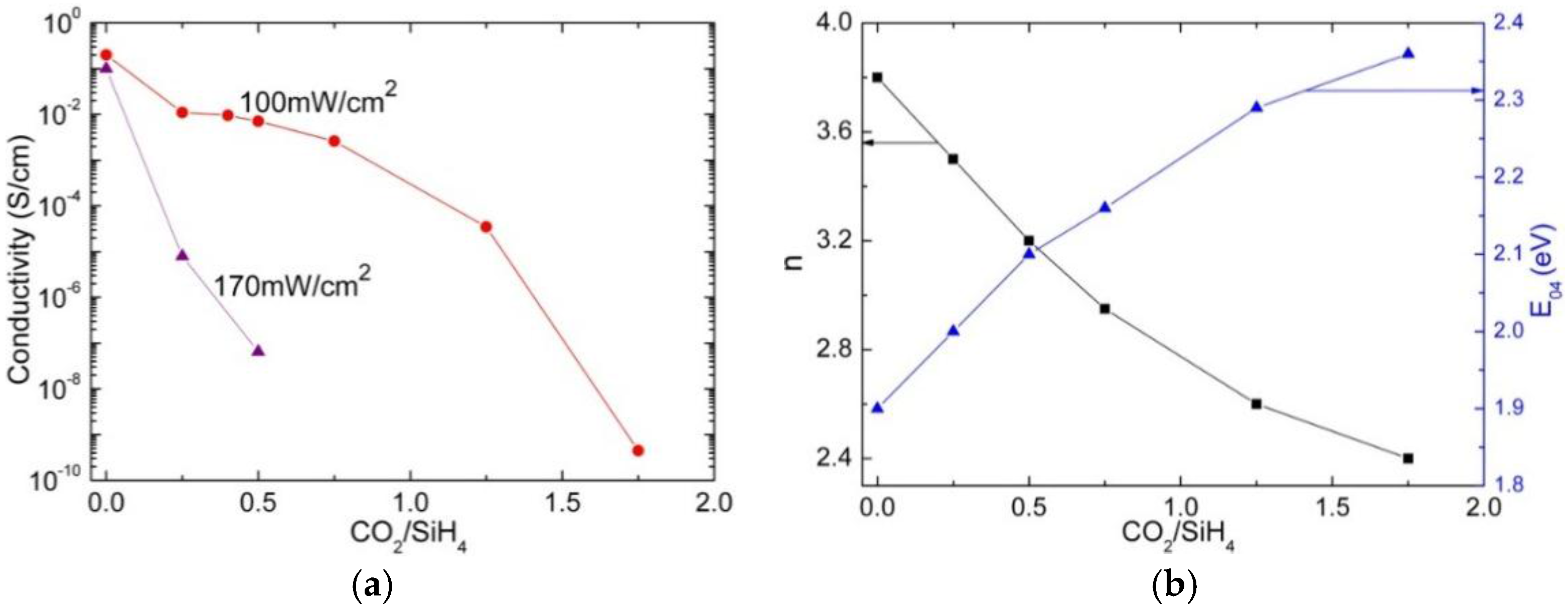
2.2.2. p-Type Material (p-SiOx)

As already mentioned for the n-type material, both optical and electrical properties are crucial in the development of p-SiOx as advanced doped layer. Again, a mixed phase structure can be beneficial, as it gives the opportunity to tune the optical properties by incorporating oxygen in the amorphous phase, while maintaining a sufficient electrical conductivity thanks to the doped nanocrystalline Si phase. Boron-doped nc-SiOx films were deposited by VHF-PECVD using CO2, SiH4, H2, and B(CH3)3 as doping gas. In this case as well the CO2/SiH4 flow rate ratio was used as the main parameter to vary the oxygen content and rather large H2 dilution was applied to favor the growth of mixed-phase material. Similar dependencies as for n-type material between PECVD deposition conditions and optoelectronic properties have been reported [19], but more extreme H2 dilutions seem to be necessary to maintain the beneficial Si nanocrystalline phase. Lower dilution values seem instead feasible at VHF regimes [10]. Here, we have selected an excitation frequency of 40 MHz, often used at production sites, where we could maintain the H2/SiH4 dilution ratio at a reasonable value of 125, thus avoiding a too strong reduction of the growth rate.
Figure 8 shows the optical and electrical properties of the films of two series grown with variable CO2/SiH4 flow rate ratio at two different discharge power levels. When more CO2 is added to the gas mixture, as the oxygen content increases in the material, the conductivity decreases by several orders of magnitude, with a faster drop for higher power (Figure 8a). This disparity with the deposition power is related to the different structural changes in the two growth regimes and to the different doping efficiency of crystalline and amorphous material. While at high power, characterized by a larger growth rate, the material becomes fully amorphous already with low CO2 flow rate, in the slower growth case the ordered phase is preserved in a wide range of CO2/SiH4. Figure 8b shows the values of refractive index at 635 nm and E04 for the most promising sample series (lower discharge power). The decrease of n down to 2.4 and the gap enlargement ΔE04 up to 0.5, as oxygen is incorporated in the material, open for possible beneficial optical effects in case of application within solar cells.
The relationship between optical and electrical properties is the central point in the development of an efficient doped layer. In superstrate-type p-i-n solar cells, the p-layer is a window layer. As high bandgap accompanied by sufficient conductivity is desired, a proper figure of merit for the material is the plot of conductivity vs. optical bandgap (E04) shown in Figure 9 (here a third sample series has been included, deposited at even lower discharge power). This shows the growth conditions where the conductivity can be sustained up to usable values within p-i-n junctions while the film becomes more transparent with oxygen intake.
The developed material has been considered as a replacement for the p-type µc-Si:H layer in single-junction μc-Si:H solar cells, also in view of future application into the μc-Si:H bottom junction of micromorph devices. Figure 10a shows the EQE of two identical solar cells with standard p-μc-Si:H and with p-SiOx front layer (same p-layer thickness). Here, the p-SiOx layer grown at 100 mW/cm2 and CO2/SiH4 = 0.75 has been selected. First of all, similar fill factors have been measured for both the cells, which is a clear indication of the appropriate electronic quality of the developed p-layer. A pronounced EQE enhancement is measured in the wavelength range up to ~500 nm, which produces a global increase of the short circuit current by 1 mA/cm2. At the same time the similar spectral response in the long wavelength region indicates a good nucleation of the i-layer (with negligible amorphous incubation layer) comparable with that obtained with standard p-μc-Si:H layer. Overall, with the enlarged EQE accompanied by similar values of VOC and FF, an increase of the conversion efficiency by ~0.3% absolute has been measured. Together with the EQE enhancement, a reduced reflection at short wavelengths has been observed by reflectance measurements on the cells (Figure 10b). The improved EQE can be thus ascribed not only to the lower parasitic absorption of the novel p-layer but also to its lower refractive index that reduces the reflection losses at the TCO/Si interface by index matching. This second effect depends on the roughness of the front electrode, and is indeed not observed with rougher TCO [10], where an efficient gradual change of refractive index is achieved.

3. Discussion

Intrinsic and doped silicon oxide alloys can be advantageously applied within thin-film Si solar cells. As for the intrinsic material, wide bandgap absorber layers can be obtained by adjusting the oxygen content, thus opening for more options in multijunction solar cells when matching the bandgaps of the active layers to the solar spectrum. In this study, we have investigated the properties of a-SiOx:H films grown by VHF-PECVD. Different deposition regimes have been investigated in order to optimize both optical and electrical properties. As a matter of fact, the challenge is to obtain a material with sufficiently good electrical properties, since the defect density generally increases with larger oxygen concentration. Different values of H2 and CO2 flow rate have been used to analyze their effect on the material properties. E04 values in the range 2–2.12 eV have been obtained, whereas the photoresponse ratio varied from three to four orders of magnitude. When applied into p-i-n solar cells, an increase of VOC has been obtained with the increase of hydrogen and/or carbon dioxide. For the cells fabricated on commercial rough substrates, starting from the open circuit voltage of 860 mV measured on the a-Si:H standard cell, VOC values up to 950 mV have been obtained. However, a reduction of the fill factor has been registered, likely due to the doped layer properties, not suitable for these wide gap absorbers. In addition, these results were obtained without dedicated buffer layers at interfaces. The use of smoother substrates, useful for triple or quadruple junctions, appropriate buffer layers at interfaces, and suitable doped layers could improve the device performance in terms of both FF and VOC, making a-SiOx:H very interesting as absorber material for application in multijunction solar cells. The VOC potential for the multi-junction application has been estimated by testing the selected a-SiOx:H material in a solar cell grown on in-house flat TCO: a VOC of ~1V has been demonstrated.
The reduction of parasitic light absorption in inactive layers is another important aspect for enhancing the performance of thin-film Si solar cells. The use of poorly absorbing doped layers is desired and doped silicon oxide is a promising material. The relationship between optical and electrical properties is crucial in the development of such novel doped layer: a high bandgap accompanied by a reasonable conductivity is desired, since the layer has to function as proper charge collector. A mixed-phase material has been developed in this case, whose crucial characteristic is the decoupling of electronic and optical functionality into two phases: the nanocrystalline Si and the amorphous oxygen-rich phases, respectively. This decoupling allows for enhanced conductivity with respect to homogeneous silicon alloys, leaving at the same time margins for adjusting the optical constants (refractive index n and extinction coefficient k) by incorporating oxygen in the oxygen-rich component.
We have explored the tunability of optical and electrical properties of PECVD-grown n-SiOx films through controlled changes of the CO2/SiH4 gas flow rate ratio. When increasing the CO2 content in the gas phase, as more oxygen is incorporated in the films, material with reduced refractive index is obtained. At the same time, the electrical conductivity decreases by various orders while the structure changes from highly crystalline to fully amorphous. For application as n-type layers in thin-film Si solar cells, particularly promising are the mixed-phase materials realized with intermediate values of the CO2/SiH4 ratio, characterized by a refractive index already well below the value for microcrystalline Si (~2.5 vs. 3.5 at 600 nm) and reasonable electrical conductivity (above 10−5 S/cm). Substitution of the conventional Si doped layers with SiOx based films, still deposited by PECVD, can be beneficial at (1) reducing the absorption losses, thanks to the lower k with respect to the Si counterpart, and (2) exploiting positive optical effects related to the lower n, such as the back-reflection of light toward active layers (due to index mismatch) and the abatement of plasmonic losses at the metal back reflecting contact. The material has been indeed successfully applied both into single-junction and micromorph tandem solar cells as superior n-type layer with such additional functionalities. In the top junction of micromorph solar cells a mild effect as intermediate reflector is observed. When used in single a-Si:H cells or in the bottom junction of micromorph devices, the n-SiOx layer also plays the role of spacer between the silicon absorber and the metal contact, with no need of an additional dedicated low-n spacer.
Analogously, mixed phase p-type SiOx films have been grown by adjusting the CO2 flow rate and the discharge power density. In this case the material was fabricated by VHF-PECVD at 40 MHz where reasonable hydrogen dilutions are feasible (H2/SiH4 was fixed at 125 in the present study). We have observed that lower discharge power density is preferred, as the growth rate needs to be sufficiently low to favor the formation of a mixed phase material. Thanks to the decoupled electronic and optical functionalities, material with considerably lower absorption and refractive index with respect to p-μc-Si:H, accompanied by electrical conductivity above 10−5 S/cm, has been obtained. When used as window layer in single-junction μc-Si:H solar cells, a significant increase of the EQE in the blue-green range has been observed with respect to the reference cell with standard p-layer. A JSC gain of 1 mA/cm2 has been measured, thanks to the lower absorption losses in the p-layer and the refractive index matching that reduces the reflection losses at the TCO/Si interface.

4. Materials and Methods

4.1. Fabrication Details of Layers and Solar Cells

Single layers and solar cells were deposited by standard PECVD (13.56 MHz) and VHF-PECVD (at 40 or 100 MHz) at a temperature of 150 °C in dedicated process chambers of a commercial cluster tool system (MVSystems Inc., Golden, CO, USA) onto 10 × 10 cm2 substrates. These were Corning Eagle XG glass for the single layers and Asahi VU-type glass, which is coated with rough fluorine-doped tin oxide as TCO layer, for the solar cells. In-house flat TCO-covered substrates have been also occasionally considered, obtained by depositing a ZnO:Al layer on glass by sputtering.
The a-SiOx:H films were deposited at 40 MHz, using a gas mixture composed of SiH4, CO2, and H2, held at a pressure of 500 mTorr. The SiH4 flow rate was kept constant at 6 sccm, whereas CO2 and H2 flow rates were varied in the range 0.5–4 sccm and 40–160 sccm, respectively. The discharge power was fixed at 28 mW/cm2. A larger value (40 mW/cm2) was occasionally used.
Phosphorus doped n-type nc-SiOx:H (n-SiOx) films were deposited at 13.56 MHz using H2, SiH4, CO2, with the addition of PH3 as doping gas. The CO2/SiH4 gas flow rate ratio was varied in the range 0–5, while keeping the PH3/(PH3 + SiH4) doping ratio fixed at 2%, the H2/SiH4 flow rate ratio at 200, the pressure at 1.9 Torr, and the plasma power density at 40 mW/cm2.
Boron-doped p-type nc-SiOx:H (p-SiOx) films were deposited at 40 MHz using SiH4, CO2, H2, with the addition of B(CH3)3 (trimethylboron—TMB) as doping gas. The H2/SiH4 dilution ratio and the TMB/SiH4 doping ratio were fixed at 125 and 5‰, respectively. The CO2/SiH4 flow rate ratio was varied from 0 to 2.25. Three discharge power densities were considered: 170 mW/cm2, 100 mW/cm2, and 55 mW/cm2.
The materials were applied into single and/or micromorph (a-Si:H/µc-Si:H) tandem superstrate-type solar cells (p-i-n). Cells with 1 cm2 area were defined by depositing the back contact (generally 80 nm-thick Al doped ZnO plus Ag, unless otherwise specified) through a metal mask.
The a-SiOx:H layer was tested as absorber layer into single junction cells with the following structure: 10 nm thick amorphous silicon-carbide p-layer, 150 nm thick amorphous silicon oxide i-layer, and 30 nm thick microcrystalline Si n-layer. Standard doped layers were applied and no buffer was included at the p-i interface in order to evaluate the absorber quality without possible influence coming from other factors. For comparison, standard a-Si:H p-i-n solar cells were fabricated with absorber layer grown at 100 MHz from SiH4 alone. More details about the deposition conditions used for doped layers and a-Si:H are reported elsewhere [20].
The n-SiOx layer was applied as alternative novel n-layer into both single a-Si:H and micromorph tandem solar cells. The thickness of the absorber layer was 350 nm for the single cells, while 250 nm and 1.7 µm were used for the a-Si:H top and μc-Si:H bottom junction in the tandem cells, respectively. In both the cases, identical devices including n-SiOx or standard μc-Si:H n-layer (n-Si) were deposited, with thickness set to 35 nm. For these cells in some cases the ZnO spacer was omitted when defining the back contact.
The p-SiOx material was tested into single μc-Si:H solar cells. These devices, with 1 μm thick absorber layer, were grown on Asahi glass coated with an additional thin ZnO layer (20 nm) to protect the tin oxide layer against the hydrogen rich plasmas. Standard 35 nm-thick μc-Si:H n-layer was applied.

4.2. Characterization Techniques

The material characterization has been carried out on ~200-nm-thick films for the a-SiOx:H layers and ~100 nm for the doped layers. Reflectance and transmittance spectra have been measured with a UV-Vis-NIR PerkinElmer λ-900 spectrophotometer (PerkinElmer Inc., Waltham, MA, USA) equipped with an integrating sphere. The refractive index n has been estimated from the interference fringes at wavelength of about 500 nm in the transmittance spectra, knowing the layer thickness. From optical reflectance and transmittance, the absorption spectra have been extracted to evaluate E04 (energy at which the absorption coefficient is equal to 104 cm−1). The optical properties of mixed-phase materials have been also investigated by spectroscopic ellipsometry. The measurements have been carried out at incident angle of 70° with a UVISEL phase-modulated ellipsometer from HORIBA Scientific. The raw data, Is = sin 2Ψ sin Δ and Ic = sin 2Ψ cos Δ, where Ψ and Δ are the ellipsometric angles (amplitude ratio and dephasing between p- and s-polarizations of light), have been treated in the Bruggeman effective medium approximation [21]. The bulk of the material has been described with a mixture of the tabulated optical constants of fine-grained c-Si [22], for the Si nanocrystal component, and an adjustable mixture of a-Si:H and/or SiO and/or SiO2 [23], for the non-stoichiometric silicon oxide matrix. The surface roughness has been accounted for by including a thin top layer with voids (~10-nm-thick from the fitting procedure). The bulk of the standard μc-Si:H films was described instead as a mixture of fine-grained c-Si, a-Si:H, and voids.
The electrical characterization has been accomplished by coplanar conductivity measurements under dark and 100 mW/cm2 illumination. The structural investigation has been performed with a Renishaw in Via Reflex Raman spectrometer using the 514 nm line of an Ar+ laser.
The solar cells have been characterized by measuring the current-voltage characteristic under illumination in standard test conditions (25 °C, AM1.5g spectrum, and 1000 W/m2) using a dual lamp WACOM solar simulator and the EQE with a Bentham PVE300 setup. The short-circuit current density (JSC) of the solar cells has been calculated by integrating the product of EQE times the incoming photon flux of the AM1.5g solar spectrum. In addition, the reflectance of selected cells was measured with a Perkin Elmer λ-900 spectrophotometer.

5. Conclusions

Intrinsic and doped silicon oxide alloys can be advantageously applied within thin-film Si solar cells. As for the intrinsic material, a promising wide bandgap absorber layer for multi-junction architectures has been demonstrated. Doped silicon oxide alloys, with mixed-phase structure have been developed, characterized by decoupling of electronic and optical functionality into the nanocrystalline Si and the amorphous oxygen-rich phases, respectively. These n-type and p-type layers present considerably lower absorption and refractive index with respect to standard Si-based films, accompanied by electrical conductivity above 10−5 S/cm. The n-SiOx layer works as an excellent substitute for the n-layer in both single and tandem cells with additional functionalities. In the top junction of micromorph solar cells, a mild effect as intermediate reflector is observed. When used in single a-Si:H cells or in the bottom junction of micromorph devices the layer also plays the role of spacer between the silicon absorber and the metal contact. This gives the opportunity to simplify the cell architecture by eliminating the dedicated ZnO spacer in the back reflecting contact, at the same time achieving even larger spectral response in case of micromorph solar cells. For the p-SiOx layer, when applied as window layer in single-junction μc-Si:H solar cells, enhanced EQE in the blue-green range has been demonstrated. These results prove the strong potential of mixed-phase doped SiOx as superior n- and p-layers in thin-film Si solar cells allowing for improved light management while keeping a simple device structure.

Acknowledgments

This work was partially supported by the Italian Ministry of Economic Development in the framework of the Operating Agreement with ENEA for Research on the Electric System and by the EC under contract number 283501 (Fast Track project). We thank G. Nicotra (CNR-IMM, Italy) for EFTEM measurements.

Author Contributions

Lucia V. Mercaldo and Paola Delli Veneri conceived and designed the experiments; Iurie Usatii fabricated the samples; all the authors contributed to the characterization and data analysis; Lucia V. Mercaldo wrote the paper.

Conflicts of Interest

The authors declare no conflict of interest.

References

  1. Haug, F.-J.; Ballif, C. Light management in thin-film silicon solar cells. Energy Environ. Sci. 2015, 8, 824–837. [Google Scholar] [CrossRef]
  2. Cashmore, J.S.; Apolloni, M.; Braga, A.; Caglar, O.; Cervetto, V.; Fenner, Y.; Goldbach-Aschemann, S.; Goury, C.; Hötzel, J.E.; Iwahashi, T.; et al. Record 12.34% stabilized conversion efficiency in a large area thin-film silicon tandem (MICROMORPHTM) module. Prog. Photovolt. Res. Appl. 2015, 23, 1441–1447. [Google Scholar] [CrossRef]
  3. Yan, B.; Yue, G.; Sivec, L.; Yang, J.; Guha, S.; Jiang, C.-S. Innovative dual function nc-SiOx:H layer leading to a >16% efficient multi-junction thin-film silicon solar cell. Appl. Phys. Lett. 2011, 99. [Google Scholar] [CrossRef]
  4. Sai, H.; Matsui, T.; Koida, T.; Matsubara, K.; Kondo, M.; Sugiyama, S.; Katayama, H.; Takeuchi, Y.; Yoshida, I. Triple-junction thin-film silicon solar cell fabricated on periodically textured substrate with a stabilized efficiency of 13.6%. Appl. Phys. Lett. 2015, 106. [Google Scholar] [CrossRef]
  5. Yunaz, I.A.; Yamada, A.; Konagai, M. Theoretical Analysis of Amorphous Silicon Alloy Based Triple Junction Solar Cells. Jpn. J. Appl. Phys. 2007, 46. [Google Scholar] [CrossRef]
  6. Inthisang, S.; Sriprapha, K.; Miyajima, S.; Yamada, A.; Konagai, M. Hydrogenated Amorphous Silicon Oxide Solar Cells Fabricated near the Phase Transition between Amorphous and Microcrystalline Structures. Jpn. J. Appl. Phys. 2009, 48. [Google Scholar] [CrossRef]
  7. Kang, D.-W.; Sichanugrist, P.; Konagai, M. Novel application of MgF2 as a back reflector in a-SiOx:H thin-film solar cells. Appl. Phys. Express. 2014, 7. [Google Scholar] [CrossRef]
  8. Kim, D.Y.; Guijt, E.; Van Swaaij, R.A.C.M.M.; Zeman, M. Development of a-SiOx:H solar cells with very high Voc × FF product. Prog. Photovolt. Res. Appl. 2015, 23, 671–684. [Google Scholar] [CrossRef]
  9. Veneri, P.D.; Mercaldo, L.V.; Usatii, I. Silicon oxide based n-doped layer for improved performance of thin-film silicon solar cells. Appl. Phys. Lett. 2010, 97. [Google Scholar] [CrossRef]
  10. Cuony, P.; Marending, M.; Alexander, D.T.L.; Boccard, M.; Bugnon, G.; Despeisse, M.; Ballif, C. Mixed-phase p-type silicon oxide containing silicon nanocrystals and its role in thin-film silicon solar cells. Appl. Phys. Lett. 2010, 97. [Google Scholar] [CrossRef]
  11. Lambertz, A.; Grundler, T.; Finger, F. Hydrogenated amorphous silicon oxide containing a microcrystalline silicon phase and usage as an intermediate reflector in thin-film silicon solar cells. J. Appl. Phys. 2011, 109. [Google Scholar] [CrossRef]
  12. Cuony, P.; Alexander, D.T.L.; Perez-Wurfl, I.; Despeisse, M.; Bugnon, G.; Boccard, M.; Söderström, T.; Hessler-Wyser, A.; Hébert, C.; Ballif, C. Silicon Filaments in Silicon Oxide for Next-Generation Photovoltaics. Adv. Mater. 2012, 24, 1182–1186. [Google Scholar] [CrossRef] [PubMed]
  13. Veneri, P.D.; Mercaldo, L.V.; Usatii, I. Improved micromorph solar cells by means of mixed-phase n-doped silicon oxide layers. Prog. Photovolt. Res. Appl. 2013, 21, 148–155. [Google Scholar] [CrossRef]
  14. Mercaldo, L.V.; Veneri, P.D.; Usatii, I.; Polichetti, T. Broadband near-field effects for improved thin-film Si solar cells on randomly textured substrates. Sol. Energy Mater. Sol. Cells 2013, 112, 163–167. [Google Scholar] [CrossRef]
  15. Shah, A. Thin-Film Silicon Solar Cells; EPFL Press: Lausanne, Switzerland, 2010. [Google Scholar]
  16. Stuckelberger, M.; Despeisse, M.; Bugnon, G.; Schüttauf, J.-W.; Haug, F.-J.; Ballif, C. Comparison of amorphous silicon absorber materials: Light-induced degradation and solar cell efficiency. J. Appl. Phys. 2013, 114. [Google Scholar] [CrossRef]
  17. Cuony, P.; Alexander, D.T.L.; Löfgren, L.; Krumrey, M.; Marending, M.; Despeisse, M.; Ballif, C. Mixed phase silicon oxide layers for thin-film silicon solar cells. MRS Proc. 2011, 1321, 349–354. [Google Scholar] [CrossRef]
  18. Haug, F.-J.; Söderström, T.; Cubero, O.; Terrazzoni-Daudrix, V.; Ballif, C. Plasmonic absorption in textured silver back reflectors of thin-film solar cells. J. Appl. Phys. 2008, 104. [Google Scholar] [CrossRef]
  19. Lambertz, A.; Finger, F.; Holländer, B.; Rath, J.K.; Schropp, R.E.I. Boron-doped hydrogenated microcrystalline silicon oxide (μc-SiOx:H) for application in thin-film silicon solar cells. J. Non-Cryst. Solids 2012, 358, 1962–1965. [Google Scholar] [CrossRef]
  20. Veneri, P.D.; Mercaldo, L.V.; Privato, C. Deposition pressure effects on material structure and performance of micromorph tandem solar cells. Renew. Energy 2008, 33, 42–47. [Google Scholar] [CrossRef]
  21. Keita, A.-S.; Naciri, A.E.; Delachat, F.; Carrada, M.; Ferblantier, G.; Slaoui, A. Spectroscopic ellipsometry investigation of the optical properties of nanostructured Si/SiNx films. J. Appl. Phys. 2010, 107. [Google Scholar] [CrossRef]
  22. Jellison, G.E.; Chisholm, M.F.; Gorbatkin, S.M. Optical functions of chemical vapor deposited thin-film silicon determined by spectroscopic ellipsometry. Appl. Phys. Lett. 1993, 62, 3348–3350. [Google Scholar] [CrossRef]
  23. Palik, E.D. (Ed.) Handbook of Optical Constants of Solids; Academic Press: Boston, MA, USA, 1985.
Figure 1. Bandgap evolution for two sample series: variable CO2 flow rate at H2 = 120 sccm (black symbols, bottom axis) and variable H2 flow rate at CO2 = 3 sccm (blue symbols, top axis).
Energies 09 00218 g001
Figure 2. External quantum efficiency (EQE) of a-SiOx:H solar cells: (a) series deposited with different CO2 values, setting H2 =120 sccm; (b) series deposited with different H2 flow rates, setting CO2 = 3 sccm. In (a) the black curve corresponds to the reference cell that uses our standard a-Si:H, with no H2 dilution, as absorber layer; the inset shows the effect of increased discharge power density for CO2 = 3 sccm.
Energies 09 00218 g002
Figure 3. Evolution of open circuit voltage (left axis) and short circuit current density (right axis) for the two cell series of Figure 2: (a) series deposited with different CO2 values, setting H2 =120 sccm; (b) series deposited with different H2 flow rates, setting CO2 = 3 sccm. The open symbols in (a) correspond to the cell with absorber layer grown at 40 mW/cm2, while in all the other cases the power density was 28 mW/cm2. The values for the a-Si:H reference cell in (a) are shown in slightly modified color to remind that the H2 dilution is different in this case.
Energies 09 00218 g003
Figure 4. J-V characteristic under AM1.5 illumination for the same a-SiOx:H solar cell grown at 28 mW/cm2 with CO2 = 3 sccm and H2 = 120 sccm on commercial rough substrate (black line) and on in-house flat ZnO:Al on glass (red line).
Energies 09 00218 g004
Figure 5. Optical, electrical and structural properties of n-type nc-SiOx:H samples grown with different CO2/SiH4 flow rate ratio: (a) refractive index at ~500 nm (black symbols, left axis) and E04 parameter (blues symbols, right axis); (b) planar electrical conductivity and energy filtered transmission electron microscopy (EFTEM) plan-view image of the sample deposited with CO2/SiH4 = 3 (the Si phase appears as white and the O-rich phase as dark in the image).
Energies 09 00218 g005
Figure 6. EQE of (a) p-i-n a-Si:H solar cells with Si- or SiOx-based n-layer and (b) micromorph tandem cells with Si- or SiOx-based n-layer in both the top and bottom junction, completed with ZnO/Ag or simple Ag back reflecting contact.
Energies 09 00218 g006
Figure 7. J-V characteristic under AM1.5 illumination for a micromorph tandem solar cell with n-SiOx layers and no ZnO buffer.
Energies 09 00218 g007
Figure 8. Optical and electrical properties of p-type mixed phase SiOx samples grown with different CO2/SiH4 flow rate ratio: (a) in-plane electrical conductivity for two sample series grown at two discharge power levels; (b) refractive index at 635 nm (black symbols, left axis) and E04 parameter (blues symbols, right axis) for the samples grown at lower discharge power.
Energies 09 00218 g008
Figure 9. Evolution of lateral conductivity with increasing bandgap (estimated in terms of E04 parameter) obtained with increasing CO2/SiH4 flow rate ratio for three sample series grown at different discharge power.
Energies 09 00218 g009
Figure 10. EQE (a) and reflectance (b) of 1 μm thick μc-Si:H solar cells on Asahi/ZnO(20 nm) with p-μc-Si:H (p-Si in the legend, black line) and p-SiOx window layer (red line).
Energies 09 00218 g010

