1. Introduction
Given Earth’s limited stores of fossil fuels and the consequences of their usage in the environment, various alternative energy sources have now been explored and developed. Unfortunately, multiple complications exist with such energy sources: for example, fuel cells and photovoltaic modules cannot accept currents in the reverse direction, do not perform well with current ripples, and have low voltage characteristics [
1,
2,
3,
4,
5,
6,
7,
8,
9,
10,
11]. For these reasons, normally a boost converter is required to step-up and regulate the input voltage to a higher value [
3,
4,
6,
7,
8,
9,
10,
11]. However, the inherent inductor current ripple of the boost converter causes a high frequency input in the current ripple [
6,
7,
9].
Various essays have been presented to solve the problems caused by the high frequency current ripple [
5,
6,
7,
8,
9,
10,
11]. Generally speaking, a large electrolytic capacitor can be used in a converter DC (direct current) link to absorb harmonics. However, an electrolytic capacitor has poor reliability, limited temperature rating, poor shelf life, higher equivalent series resistance (ESR), and is large in size. In [
5], a high frequency active filter is adopted as a solution to eliminate the DC link electrolytic capacitor. This solution has been verified by simulation studies on a three-phase pulse-width modulation (PWM) inverter system.
One common method is to adopt interleaved boost converters to minimize the high frequency input ripples [
8,
9,
10,
11]. Nevertheless, the interleaved control still suffers from several disadvantages. First, as a single converter module, it is not possible to implement the corresponding interleaved control strategy. Second, there is no guarantee that the various inductors have identical characteristics, so harmonic current elimination may not be optimal and current balancing issues should be considered [
8,
10,
11].
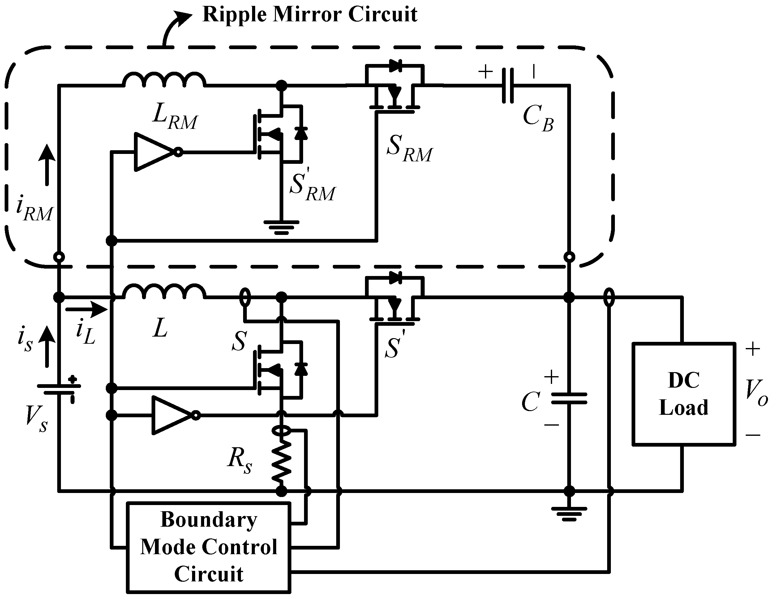
In [
7], a mirror of the boost converter called “Ripple Mirror (RM) Circuit” is introduced and this structure presents the other drawback to be only efficient in steady-state and continuous conduction mode (CCM) operation. In addition, experimental results are lacking in this essay and the estimated conversion efficiency is relatively low due to hard switching.
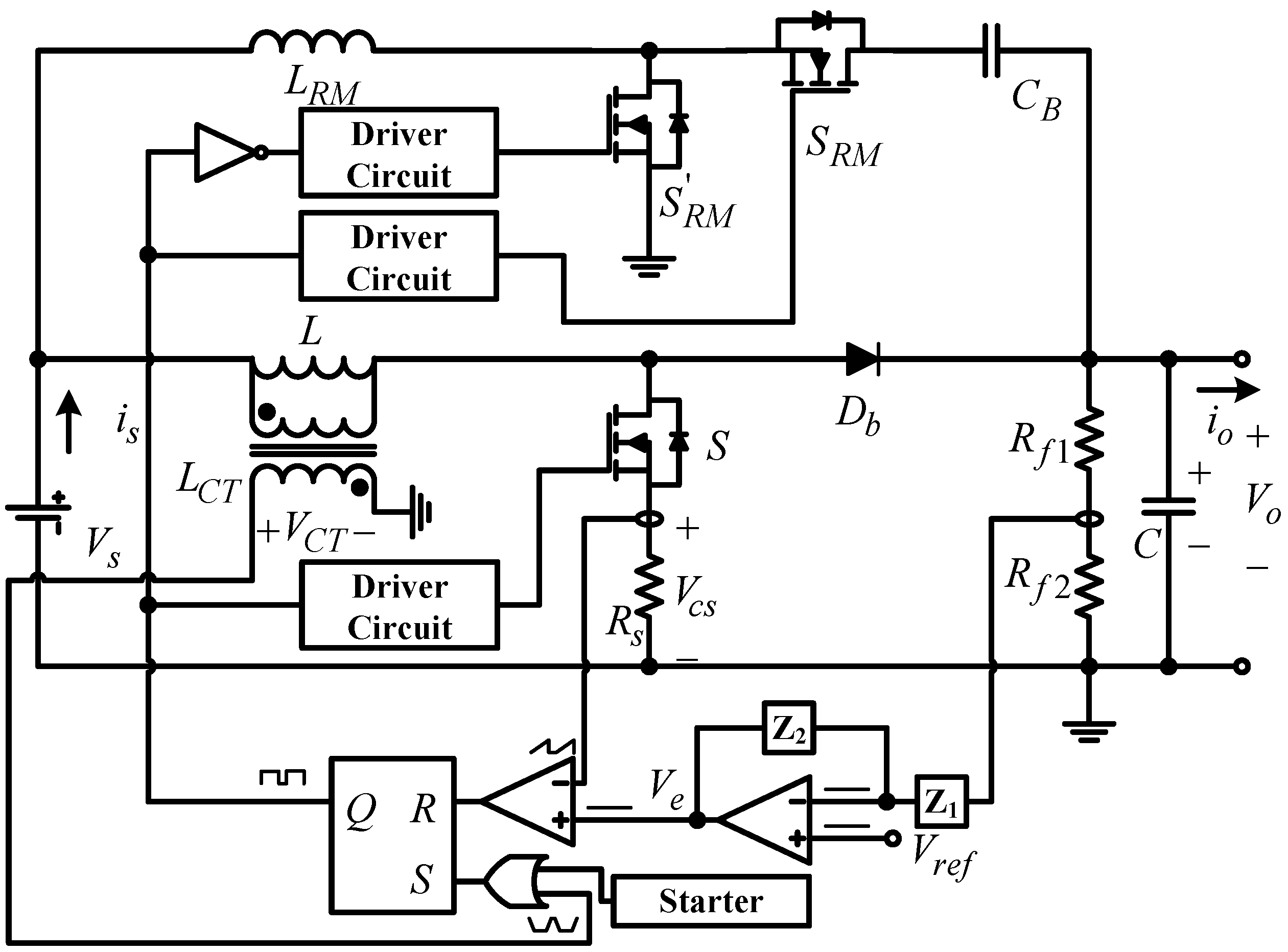
In this paper, a ZVS (zero voltage switching)/ZCS (zero current switching) boost converter with RM circuit and boundary-mode control to achieve the zero input current ripple is presented. It is found that the proposed RM circuit technique can provide a much better flexibility than the two-phase interleaved boost converter for locating the zero ripple operating point in the design stage. In addition, the choice of using a boundary-mode control is mainly due to taking in the consideration the achieving of both ZVS/ZCS soft-switching and constant on-time control for the converter. An experimental 200 W power rating prototype is constructed, and the measured results indeed verify the effectiveness of the proposed converter.
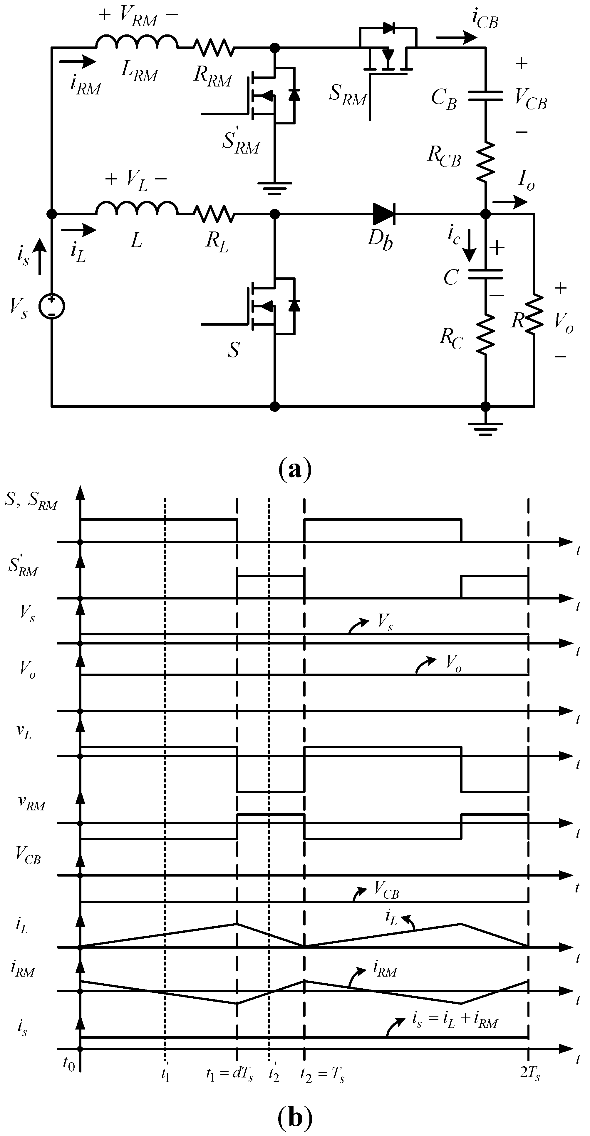
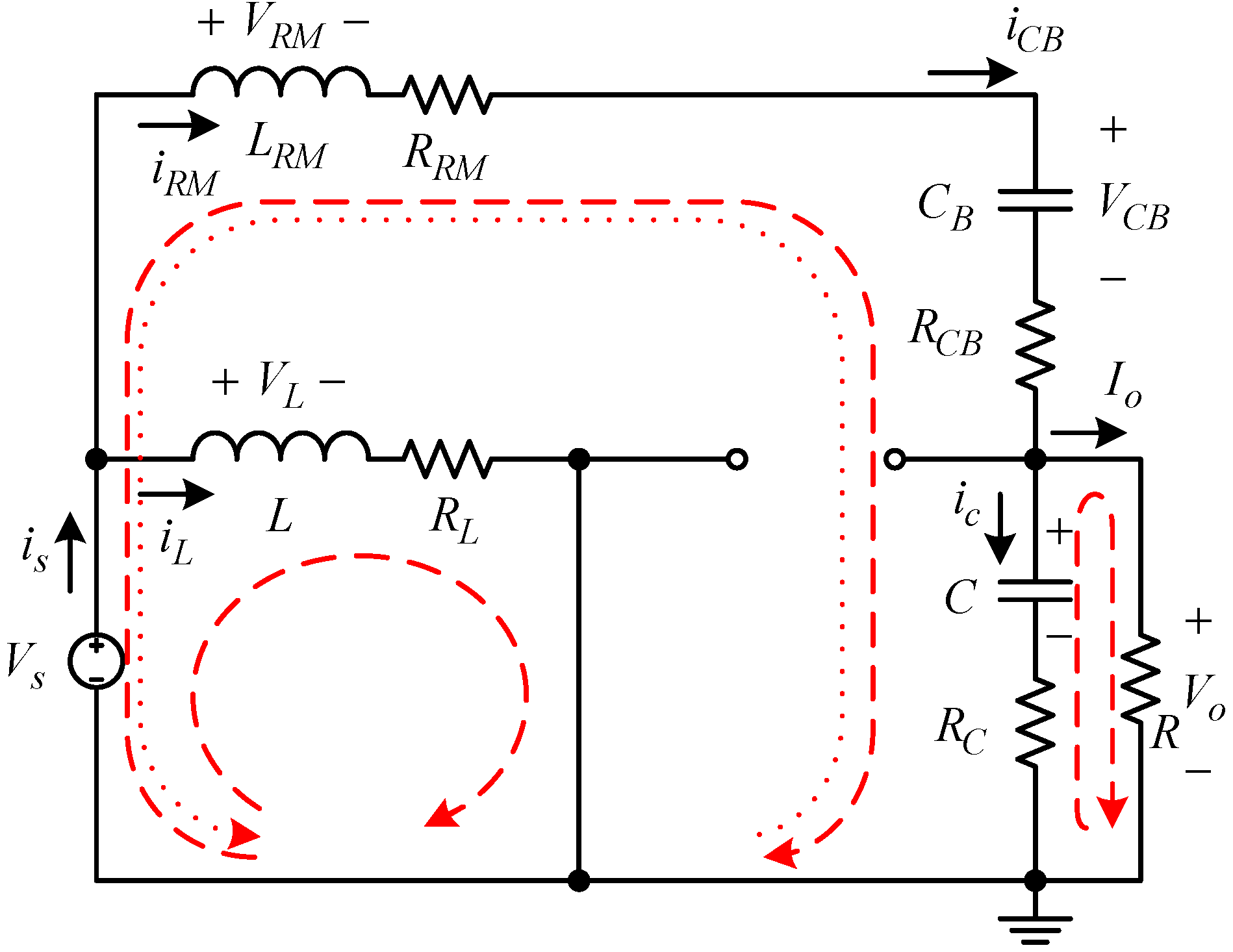
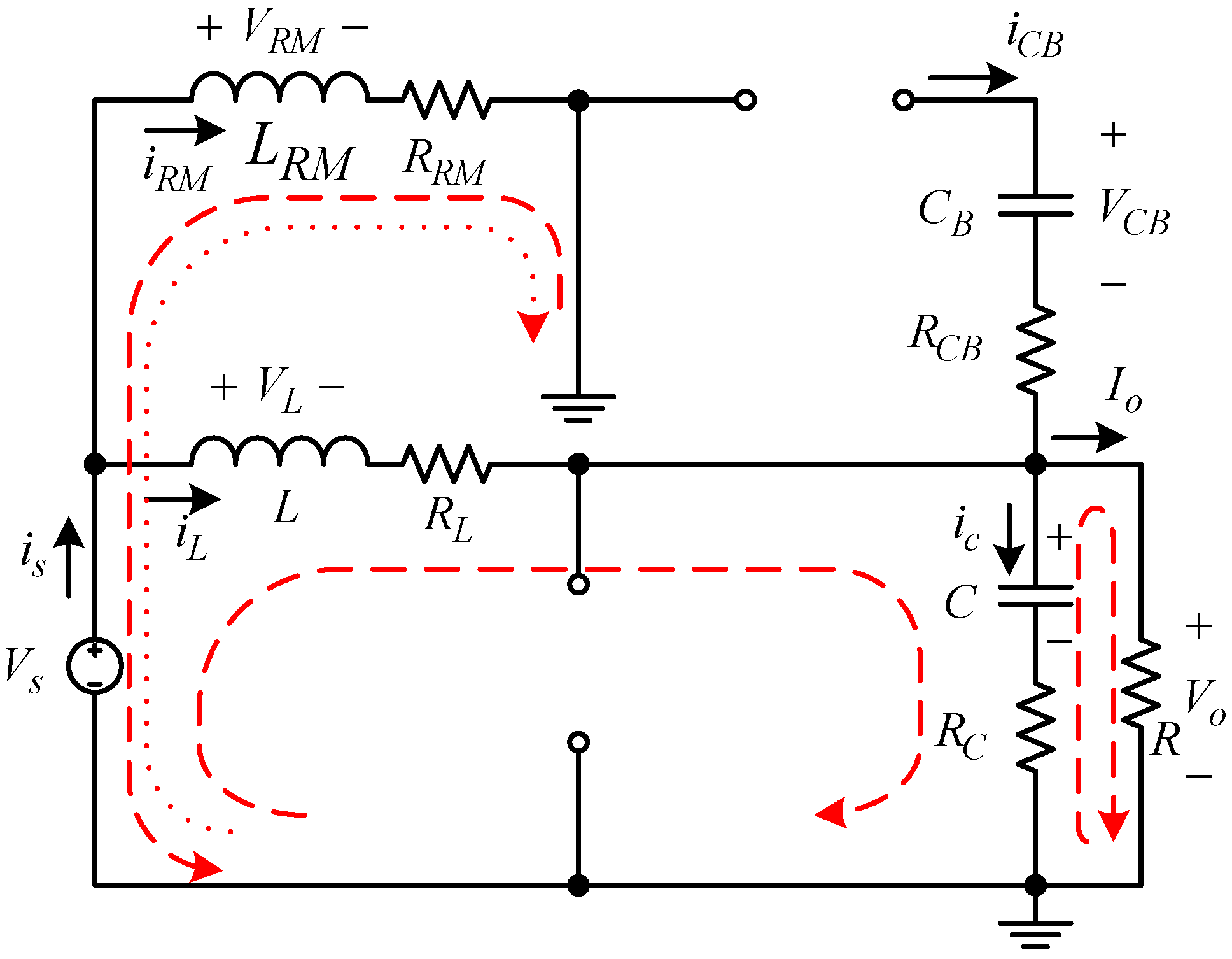
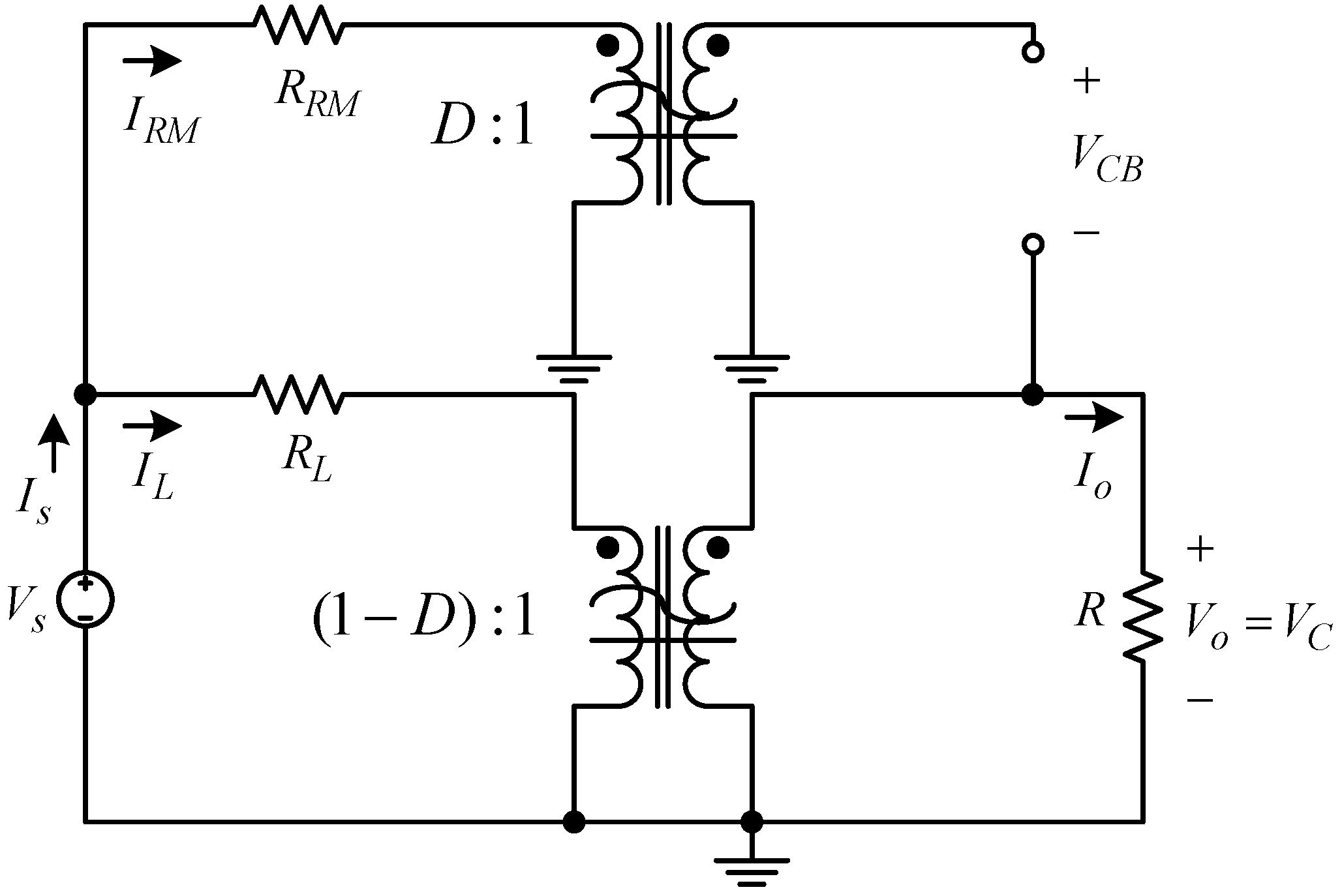
3. Analysis, Design and Control Strategy of Proposed Topology
3.1. Analysis of the Boost Converter
From
Figure 3b, one can see that the input current
is can be regarded as a pure DC value. The steady-state main inductor current
IL equals the sum of the inductor current
iL and the ripple mirror inductor current
iRM. Thus, one can derive the relationship between the main inductor
L and the ripple mirror inductor
LRM by the sum of
diL/
dt and
diRM/
dt from the circuit Equations (1) and (2), allow the result to be zero to achieve the following equation:
From Equation (31), it can be easily found that the inductance of the ripple mirror inductor
LRM is dependent upon the voltage across ESRs of the inductors, namely
RL and
RRM, and the designed duty ratio
Ddr. Furthermore, if the designed duty ratio
Ddr is over than 0.5, the inductance of the ripple mirror inductor
LRM will be smaller than that of the main inductor
L. The input current ripple, Δ
is of the proposed converter can be derived as follows:
In Equation (32), the magnitude of the peak to peak input current ripple is dependent upon the designed duty ratio
Ddr. When
Ddr equals
d and when assuming
RL ×
IL equals zero, the peak to peak input current ripple equals zero. Hence, one can design the zero input current ripple operating point at the desired point. To further understand, a converter prototype with 48 V input, 200 V/200 W output, and switching frequency of 20 kHz specifications, is used to illustrate it, where the resistance of ESR of the is equal to 0.3 Ω and resistance of the output resistor R is equal to 200 Ω. The dissipation term
RLIL/
Vs of the system is about 0.025. Substituting the per unit values of the input current ripple Δ
is, the input voltage
Vs, the operation period
Ts, and the inductance of the main inductor
L into Equation (32) and let the design operating point
Ddr be 0.75, one can obtain the following result:
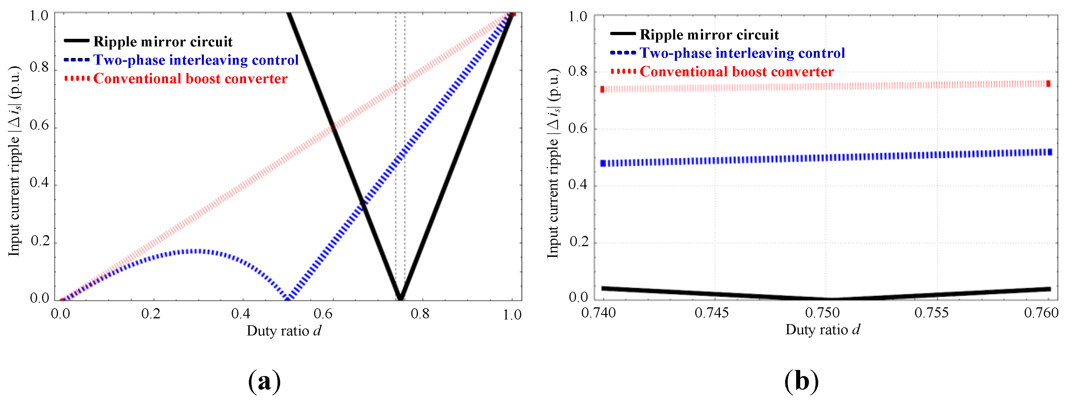
Figure 7a shows the absolute value of the peak to peak input current ripple, |Δ
is|,
versus duty ratio
d with three different techniques. The proposed converter has a smaller input current ripple as compared with the two-phase interleaving control and the conventional boost converter when the duty ratio
d is over 0.67. A better view of the ripple canceling capability around the duty ratio
d of 0.75 is shown in
Figure 7b. It can be seen that the proposed ripple mirror circuit technique possesses a much better ripple canceling capability than others around the designed operating point. Furthermore, unlike the fixed ripple canceling capability curve of the two-phase interleaving control, the proposed ripple mirror circuit shows a much better flexibility of being able to locate the zero input current ripple operating point dependent upon different designs. That means the |Δ
is| curve of the entire converter can be moved to the left or to the right side depending on the design.
Figure 7.
The absolute value of the input current ripple, |Δis|, versus the duty ratio d with different techniques. (a) With full range of duty ratio d and (b) around the duty ratio d = 0.75.
Figure 7.
The absolute value of the input current ripple, |Δis|, versus the duty ratio d with different techniques. (a) With full range of duty ratio d and (b) around the duty ratio d = 0.75.
3.2. Design Considerations of Main Components for the Boost Converter
The duty ratio
D is determined by the voltage gain of the proposed converter as shown in Equation (25). Considering the voltage drop on ESR of the main inductor, the duty ratio is
D = 0.76. Thus, the inductance of the main inductor can be derived as follows:
The minimum capacitance of the main capacitor
C can be found from the equation of the output voltage ripple of the boost converter as follows:
However, because the ESR of the main capacitor C will enlarge the output voltage ripple, which may also influence the performance of the feedback control loop, the minimum capacitance may not be applied. Hence, one can select a much larger capacitance C = 330 μF of the main capacitor to have a better output voltage ripple and a better feedback control loop performance. For the power MOSFET S and diode Db, to avoid overheating of the component, the product of the current stress and the on-resistance of the power MOSFET should be about 50% lower than the power dissipation limit for the power MOSFET S and the current stress of the power diode should be 50% lower than the forward current limit for the diode Db.
3.3. Design Considerations of Main Components for the Ripple Mirror Circuit
The inductance of the ripple mirror inductor
LRM can be found from Equation (31) as follows:
Likewise, the voltage stress of the blocking capacitor
CB can be found from Equation (27) as follows:
We select a capacitor with over 200 V rated voltage and about 10 μF. This is enough to clamp a smooth voltage in switching cycles and lessen the LC resonance effect caused by the blocking capacitor CB and ripple mirror inductor LRM. For the power MOSFETs of the ripple mirror circuit, namely SRM and S'RM, the current stress and the voltage stress are about a half times large than the boost converter power MOSFET S. However, because of the switching loss caused by the hard switching, the avalanche capability is much more important to these power MOSFETs. Thus, one can apply smaller gate resistor and a high speed MOSFET to lessen the crossover region of the drain to source voltage and current, which may also have better synchronization with the power MOSFET S of the boost converter.
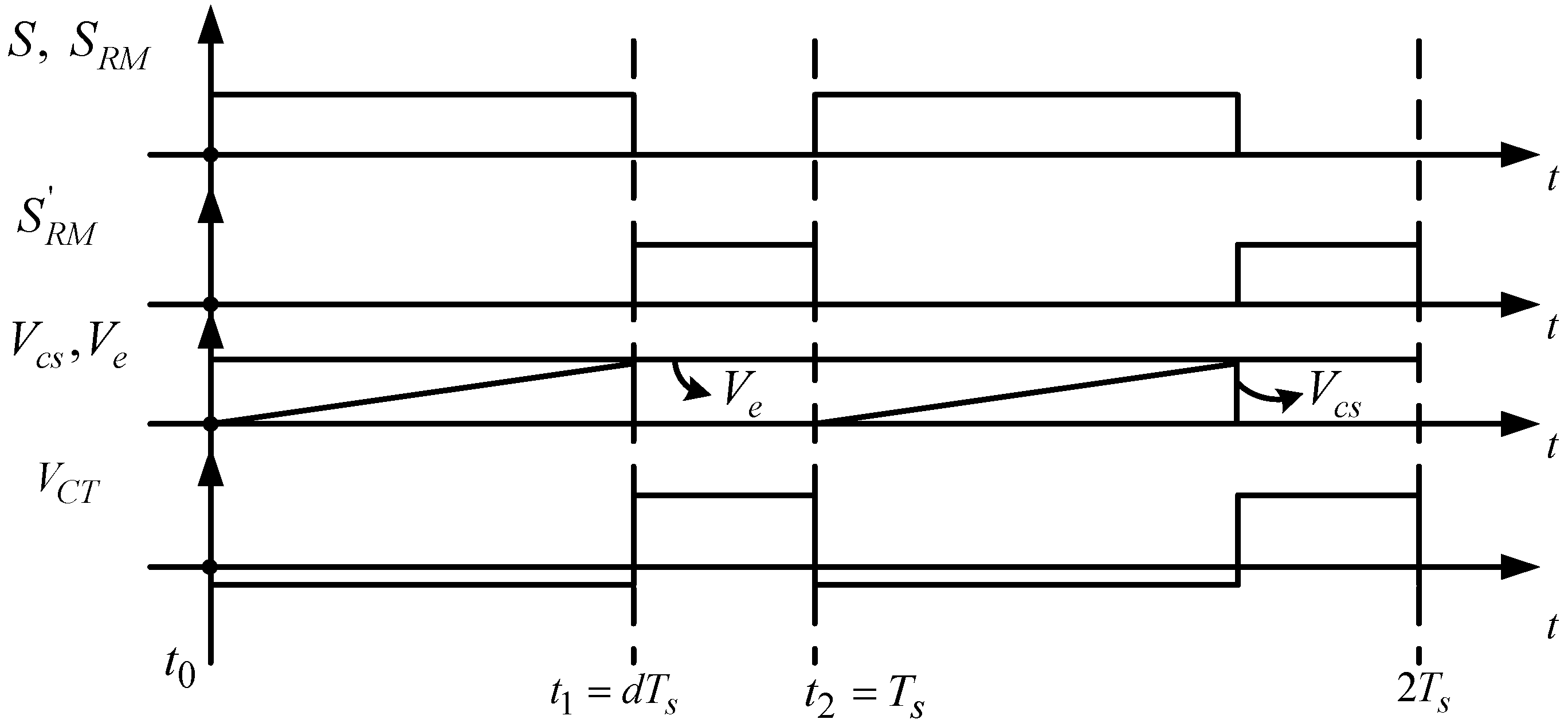
3.4. Control Strategy Realization of the Proposed Converter
As illustrated, the adopted boundary-mode control strategy is shown in
Figure 8, as well as the corresponding control signals in
Figure 9. From
Figure 9, one can see that the turn-on of the MOSFETs is coincidental with the zero crossing detection signal generated by the current transformer
LCT. In other words, the MOSFETs turns on when the voltage across the inductor
VCT crosses the zero from negative to positive. However, the turn-off of the MOSFETs is similar to that of an average current mode control. Note that the starter will be bypassed either after the boost converter is starting up or when the switching frequency
fsw is over 15 kHz.
Figure 8.
Realization diagram of the proposed boundary-mode control strategy.
Figure 8.
Realization diagram of the proposed boundary-mode control strategy.
Figure 9.
Control signals of the adopted boundary-mode control strategy.
Figure 9.
Control signals of the adopted boundary-mode control strategy.
By applying the boundary-mode control, the turn-on of all MOSFETs in every switching cycle can be maintained unchanged. This means that the ripple canceling capability of the RM circuit will remain effective under all load conditions. It is worth mentioning some other features as well. First, the control circuit does not need an external compensation signal when the duty ratio d of the proposed converter is over 50% because the current error of the main inductor L, generated by disturbance, will reset every switching cycle; therefore the problem of stability is nonexistent. Second, both zero voltage switching (ZVS) turn-on of the power MOSFETs and zero current switching (ZCS) turn-off of the diode Db of the proposed converter can be achieved naturally. The soft-switching capability can enhance the conversion efficiency by lessening both the switching loss and the reverse recovery loss. Third, the size of the main inductor L can be made smaller than that of the CCM control and contribute to the reducing of conduction loss as well. Hence, it is seen that the boundary-mode control is especially suitable for the proposed converter where not only the on-time can be fixed but also many additional advantages mentioned above can be fully utilized.
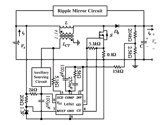
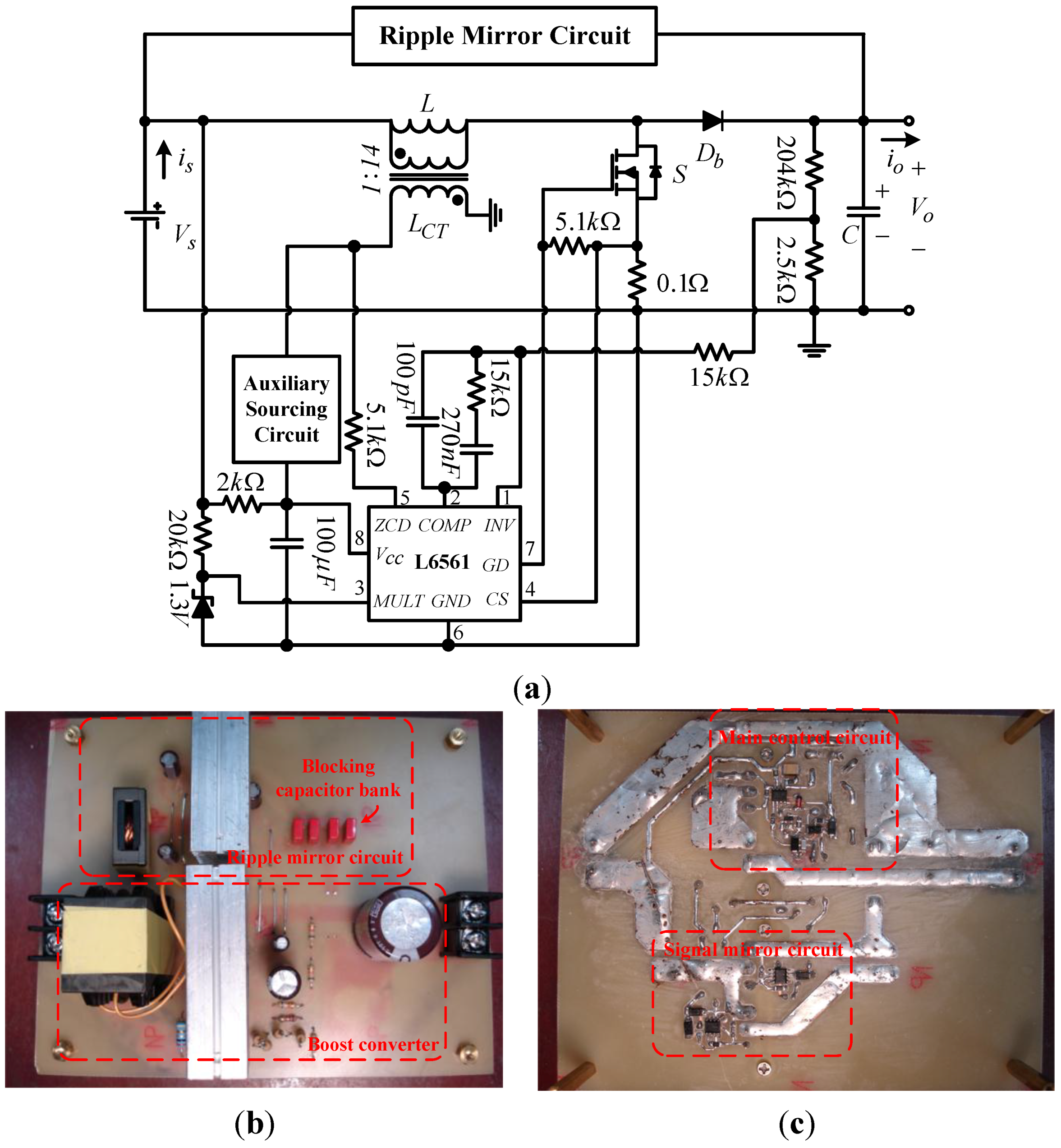
4. Experimental Results
Table 1 shows the specification of experimental prototype of the proposed converter. The main control circuit is implemented by the L6561 controller of STMicroelectronics (Geneva, Switzerland) which is wildly used for controlling boost converter under boundary-mode conditions. The circuit schematic of proposed converter prototype is implemented as shown in
Figure 10a.
Table 1.
Specifications of the proposed converter.
Table 1.
Specifications of the proposed converter.
| Specifications | Values |
|---|
| Input Voltage | 48 V |
| Output Voltage | 200 V |
| Output Voltage Ripple | ≤0.1% |
| Rated Output Power | 200 W |
| Rated Switching Frequency | 20 kHz |
Figure 10.
Experimental prototype of the proposed converter: (a) the circuit schematic; (b) top side view and (c) bottom side view.
Figure 10.
Experimental prototype of the proposed converter: (a) the circuit schematic; (b) top side view and (c) bottom side view.
The power circuit which contains the main inductor
L and the main capacitor
C is on the top side of the printed circuit board (PCB) with through-hole components for well thermal management as shown in
Figure 10b. The control circuit of the proposed converter is on the bottom side of the PCB with surface-mount components to lessen the parasitic effect and noise which may occur in the control circuit as shown in
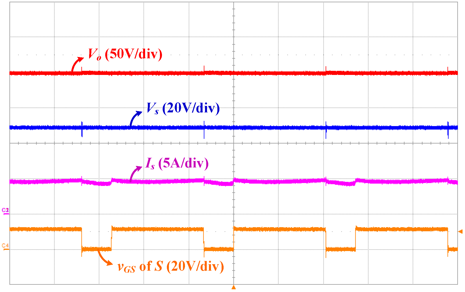
Figure 10c. From
Figure 11, one can see that with a resistive voltage sensor and voltage feedback control, the output voltage experimental waveform of the proposed converter is about 200 V. Also, less than 1% output voltage ripple fits in with the specification showed in
Table 1.
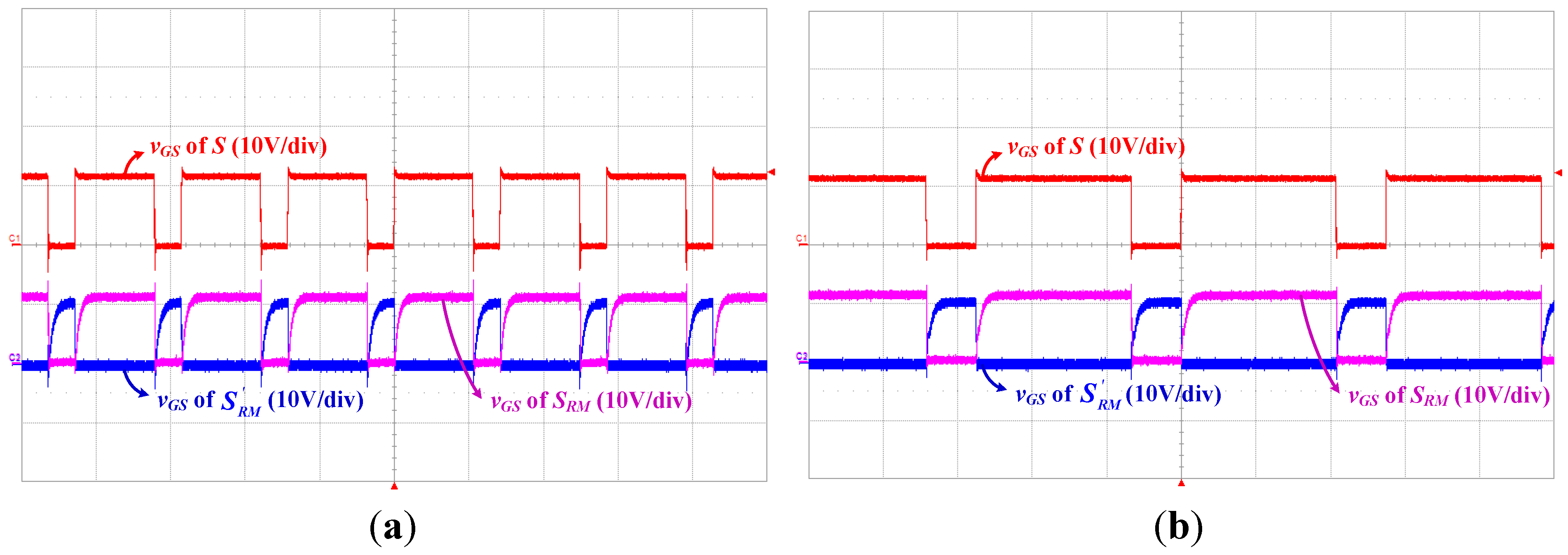
The experimental gate signal
vGS waveforms of the MOSFETs, among the main switch
S, the RM switch
SRM, and the complementary RM switch
S'
RM, are shown in
Figure 12. From
Figure 12a and
Figure 12b, it can be found that the switching frequency
fsw, under a full load condition, is merely half of the under half load condition. Also, with the cursor tools of the LeCroy wave runner, one can obtain the on-time delay of the MOSFETs of the RM circuit as about 562 ns and the off-time delay of the MOSFETs of the RM circuit as about 166ns compared with the
vGS waveform of the main switch
S.
Figure 11.
The output voltage waveform of the proposed converter under full load condition (50 ms/div).
Figure 11.
The output voltage waveform of the proposed converter under full load condition (50 ms/div).
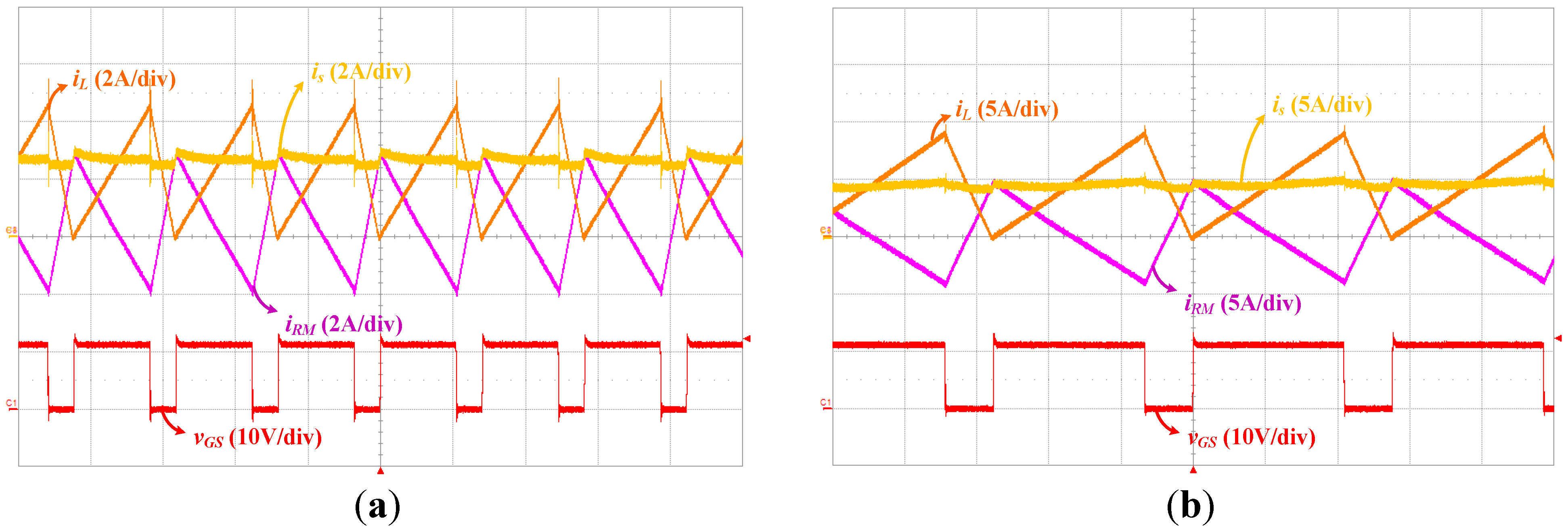
Figure 13 shows the current waveforms under half load and full load conditions. The proposed converter has an excellent ripple canceling capability under half load and full load conditions because of the constant on-time of the MOSFETs which is invariant to any load conditions by applying a boundary-mode control strategy.
Figure 12.
Gate signal waveforms of the proposed converter under (a) half, and (b) full load conditions (50 ms/div).
Figure 12.
Gate signal waveforms of the proposed converter under (a) half, and (b) full load conditions (50 ms/div).
Figure 13.
Current waveforms of the proposed converter under (a) half, and (b) full load conditions (50 ms/div).
Figure 13.
Current waveforms of the proposed converter under (a) half, and (b) full load conditions (50 ms/div).
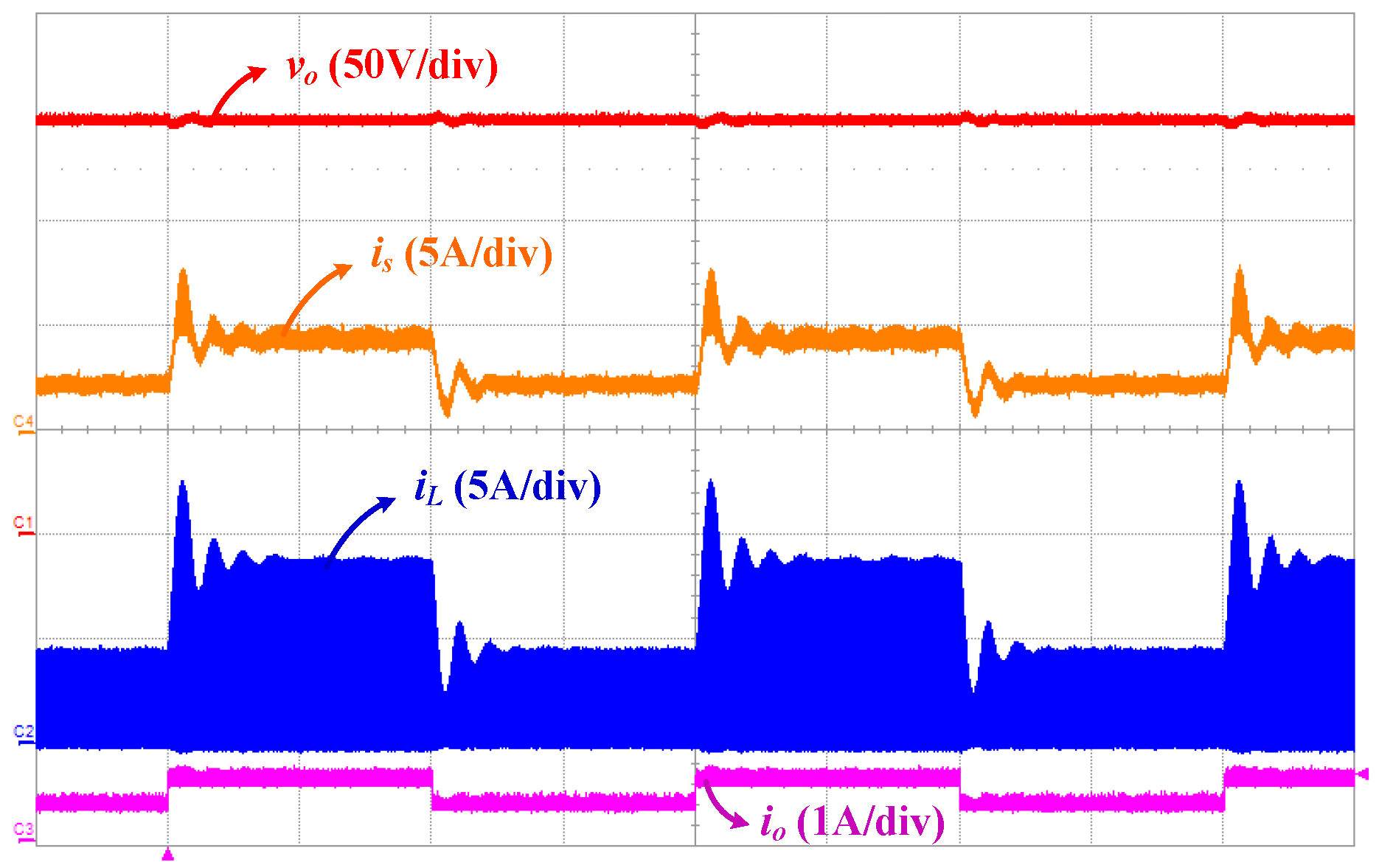
Figure 14 shows the measured waveforms of an output voltage and output current, an input current and inductor current of the proposed converter under the dynamic load change between half load and full load conditions. From the same figure, it can be seen that the output voltage almost remains a constant value which only has a slight disturbance when the load is changed.
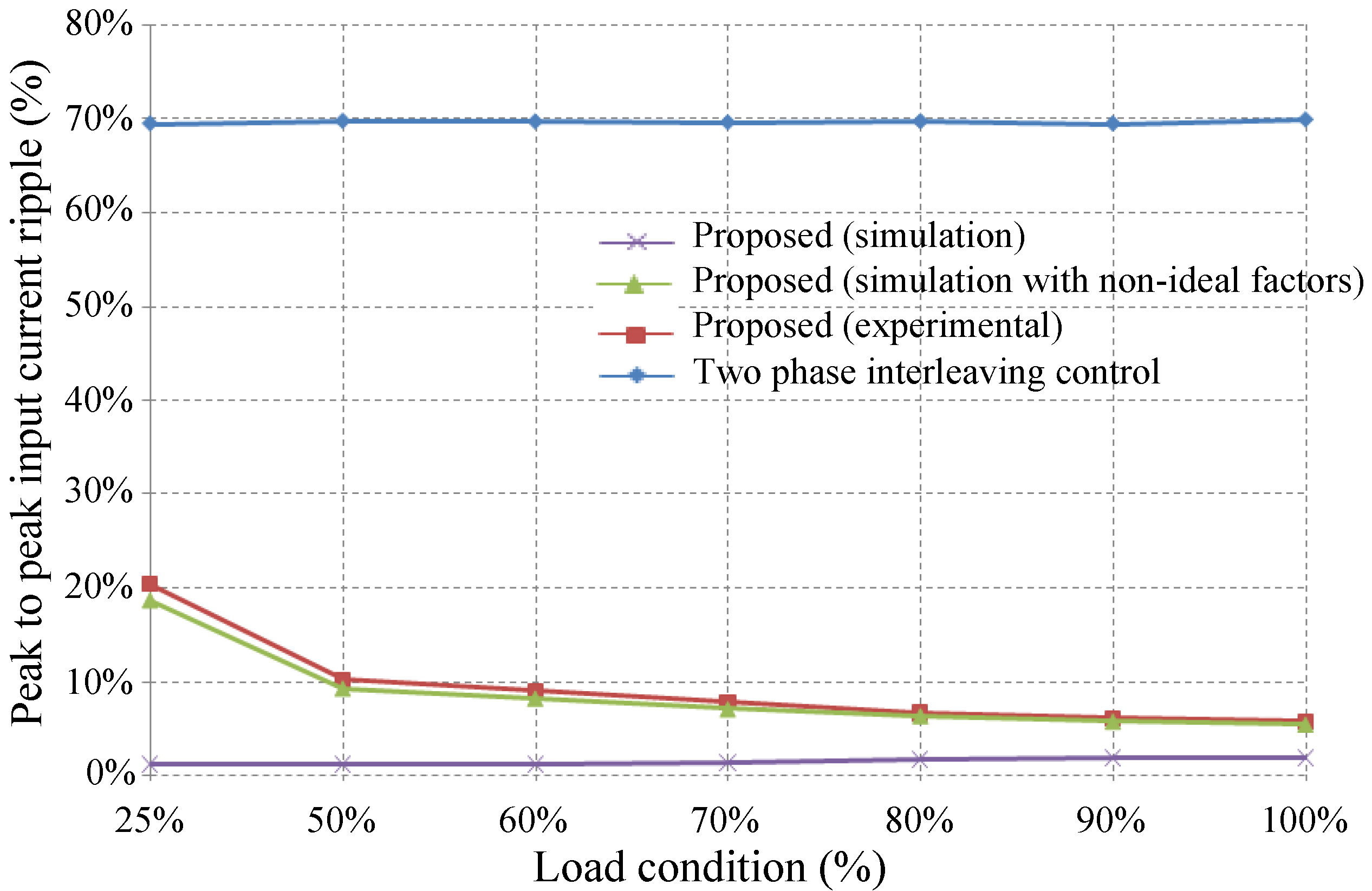
Figure 15 shows the peak to peak input current ripple under several load conditions. Comparing the results of the ripple canceling capability which contains boost converters with two phase interleaving control, the proposed converters are shown in the same table and the same figure with the same power capacity. The peak to peak input current ripple of the proposed converter is much lower than that of the boost converters with two phase interleaving control strategy, even under the worst scenario which is under 25% load condition.
Figure 14.
The measured waveforms of the proposed converter under dynamic load change (100 ms/div).
Figure 14.
The measured waveforms of the proposed converter under dynamic load change (100 ms/div).
Figure 15.
Peak to peak input current ripple under different loads.
Figure 15.
Peak to peak input current ripple under different loads.
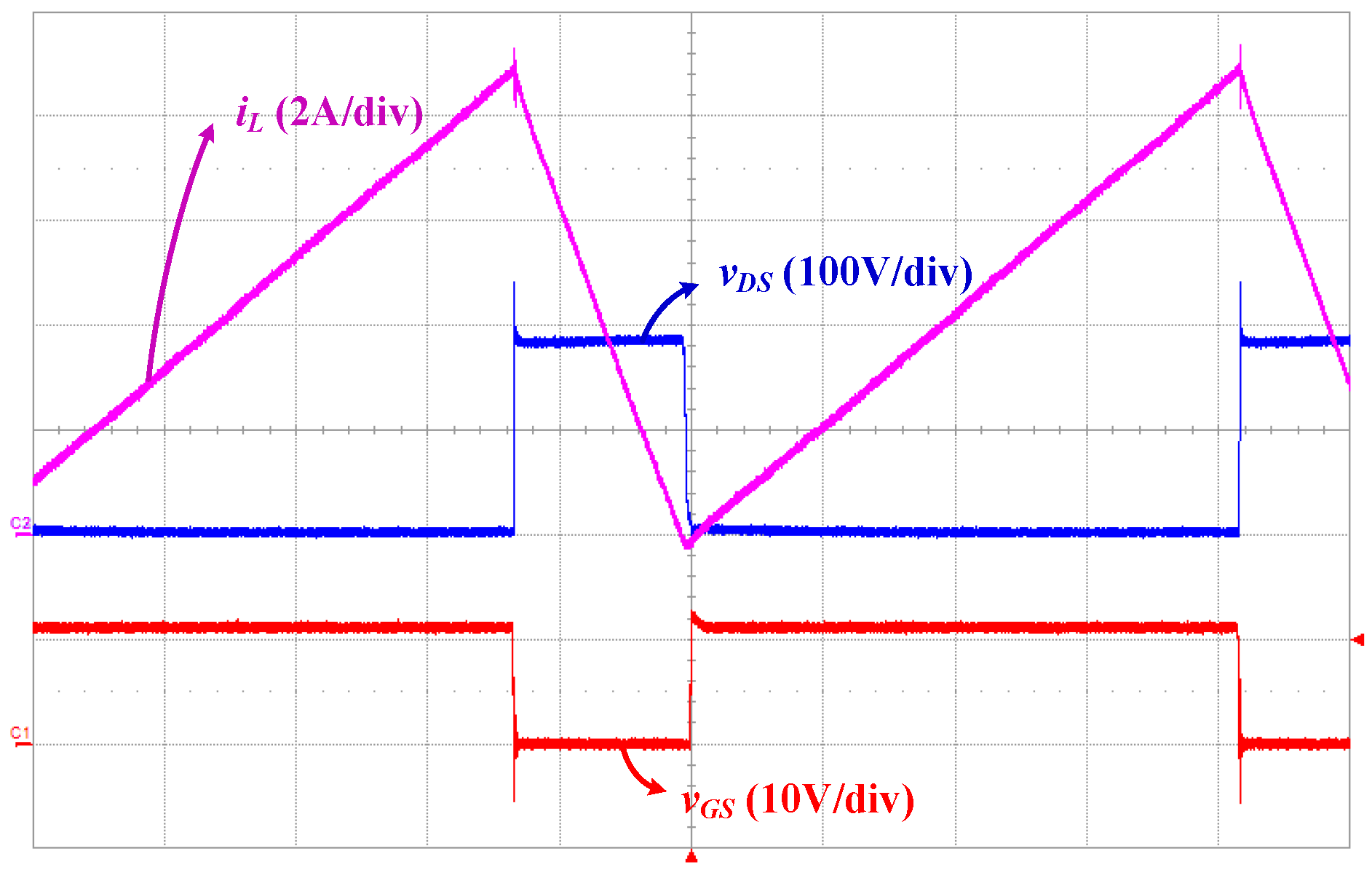
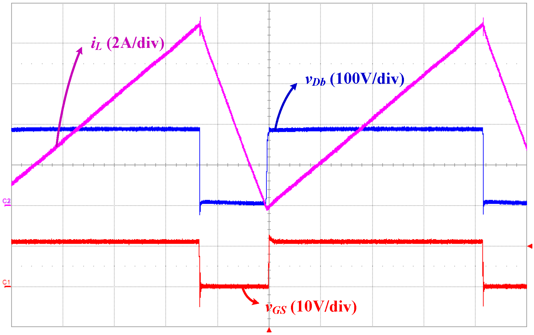
By applying the boundary-mode control strategy, the main switch
S can be turned on with zero voltage switching naturally as shown in
Figure 16. As well as the power diode
Db being turned off naturally with zero current switching as shown in
Figure 17. Both the soft switching on the main switch
S and the power diode
Db may lessen the switching loss of the proposed converter. Hence, the proposed converter can have better efficiency.
Figure 16.
The turn-on ZVS waveform of the main switch S under full load conditions (20 ms/div).
Figure 16.
The turn-on ZVS waveform of the main switch S under full load conditions (20 ms/div).
Figure 17.
The turn-off ZCS waveform of the power diode Db under full load conditions (20 ms/div).
Figure 17.
The turn-off ZCS waveform of the power diode Db under full load conditions (20 ms/div).
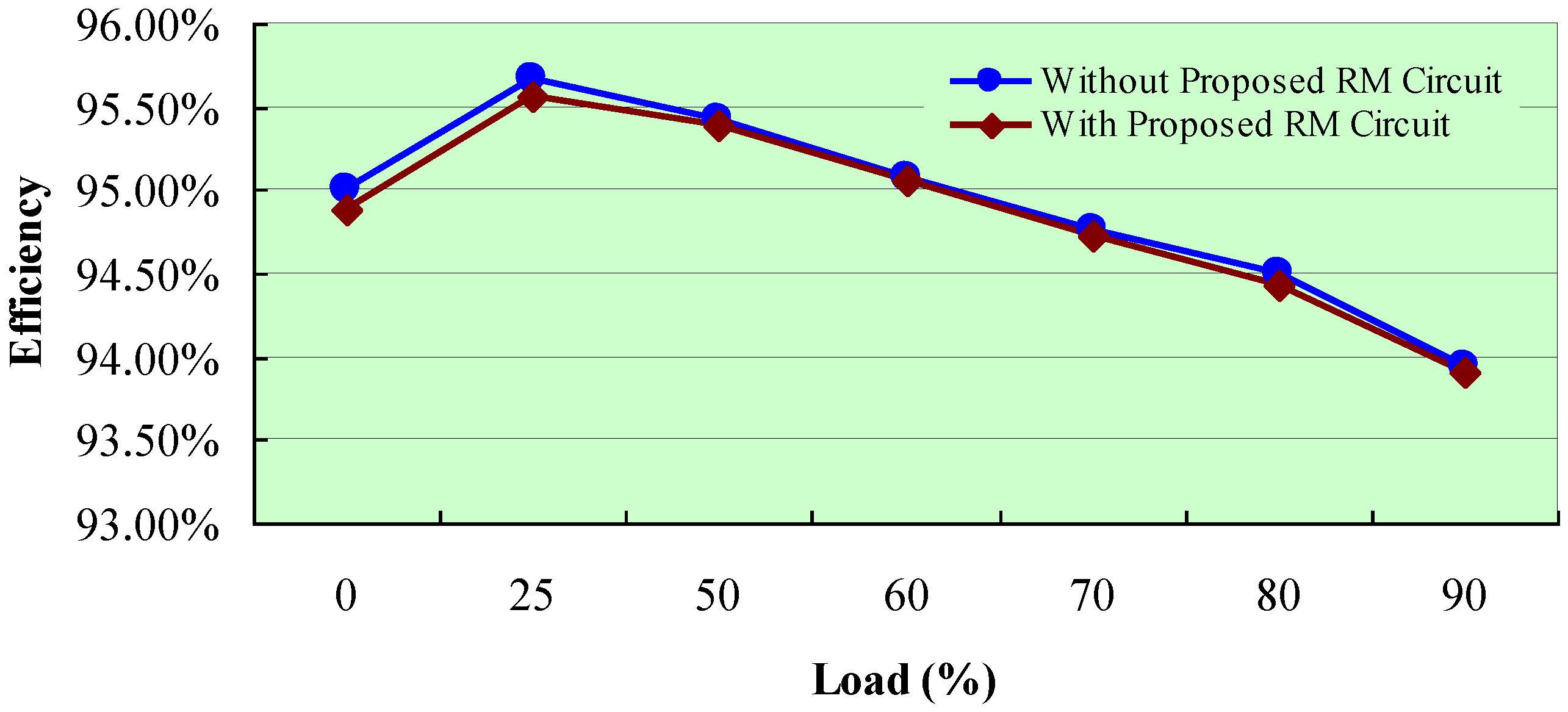
Table 2 shows the measured efficiency records of the proposed converter. For comparison, the experimental results of a conventional converter without RM circuit are also shown in the same table. In
Table 2, one can see that the proposed converter has best efficiency of 95.57% under a half load condition. The worst efficiency which is 93.9%, is obtained under full load condition. The contents of
Table 2 can be expressed as shown in
Figure 18. The efficiency curve of the proposed converter is very close to that without a RM circuit. The largest difference between the two curves occurs in a 25% load condition which is about 0.11%. One can see that the proposed low power ripple mirror circuit only processes ripple power, so the entire efficiency is just slightly influenced.
Table 2.
Efficiency records under different load conditions.
Table 2.
Efficiency records under different load conditions.
| Load Conditions | Without RM | With RM |
|---|
| 25% load | 95.00% | 94.89% |
| 50% load | 95.67% | 95.57% |
| 60% load | 95.42% | 95.39% |
| 70% load | 95.07% | 95.05% |
| 80% load | 94.76% | 94.72% |
| 90% load | 94.50% | 94.43% |
| Rated load | 93.94% | 93.90% |
Figure 18.
Efficiency comparison for the constructed experiment prototype with and without the proposed RM circuit.
Figure 18.
Efficiency comparison for the constructed experiment prototype with and without the proposed RM circuit.


