
Recent Progress and Challenges in Controlling Secondary Phases in Kesterite CZT(S/Se) Thin Films: A Critical Review


Abstract
:1. Introduction
2. Deposition Techniques
2.1. Solution-Based Approaches
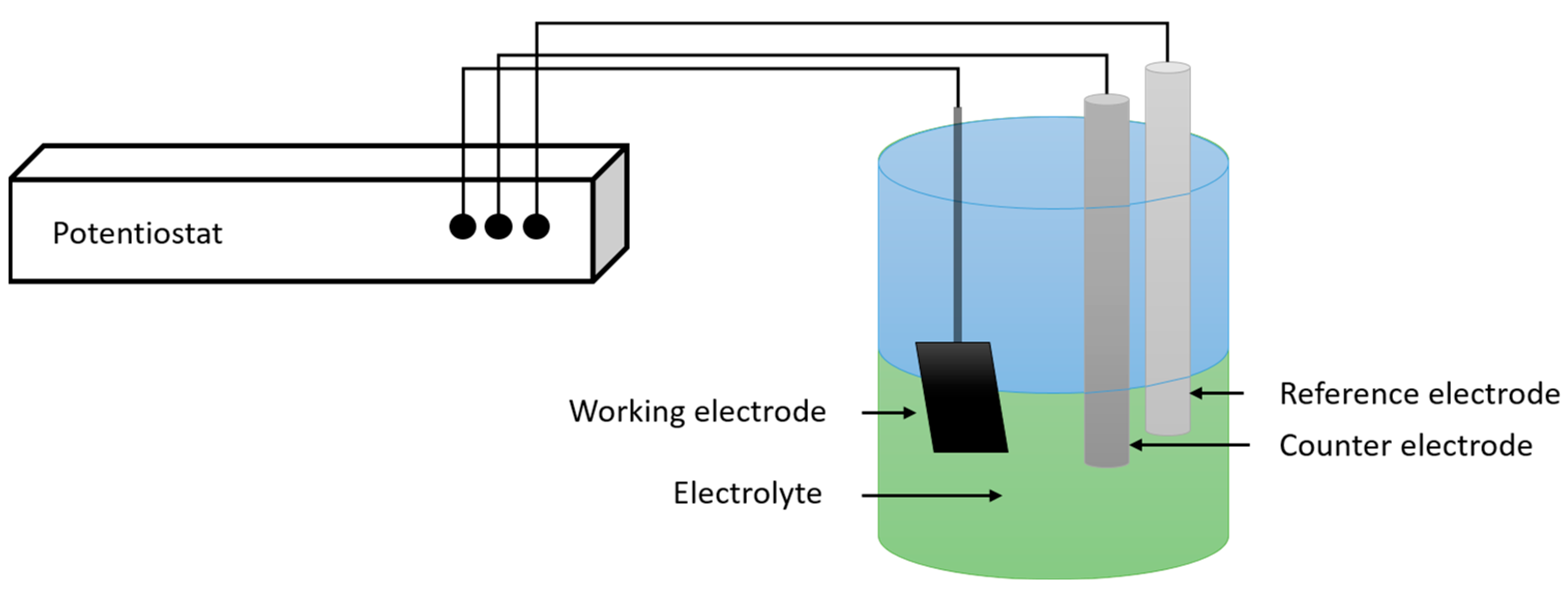
2.1.1. Electrodeposition
2.1.2. Sol-Gel
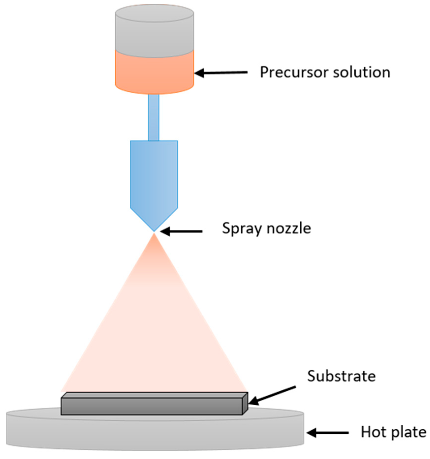
2.1.3. Spray Pyrolysis
2.2. Physical-Based Approaches
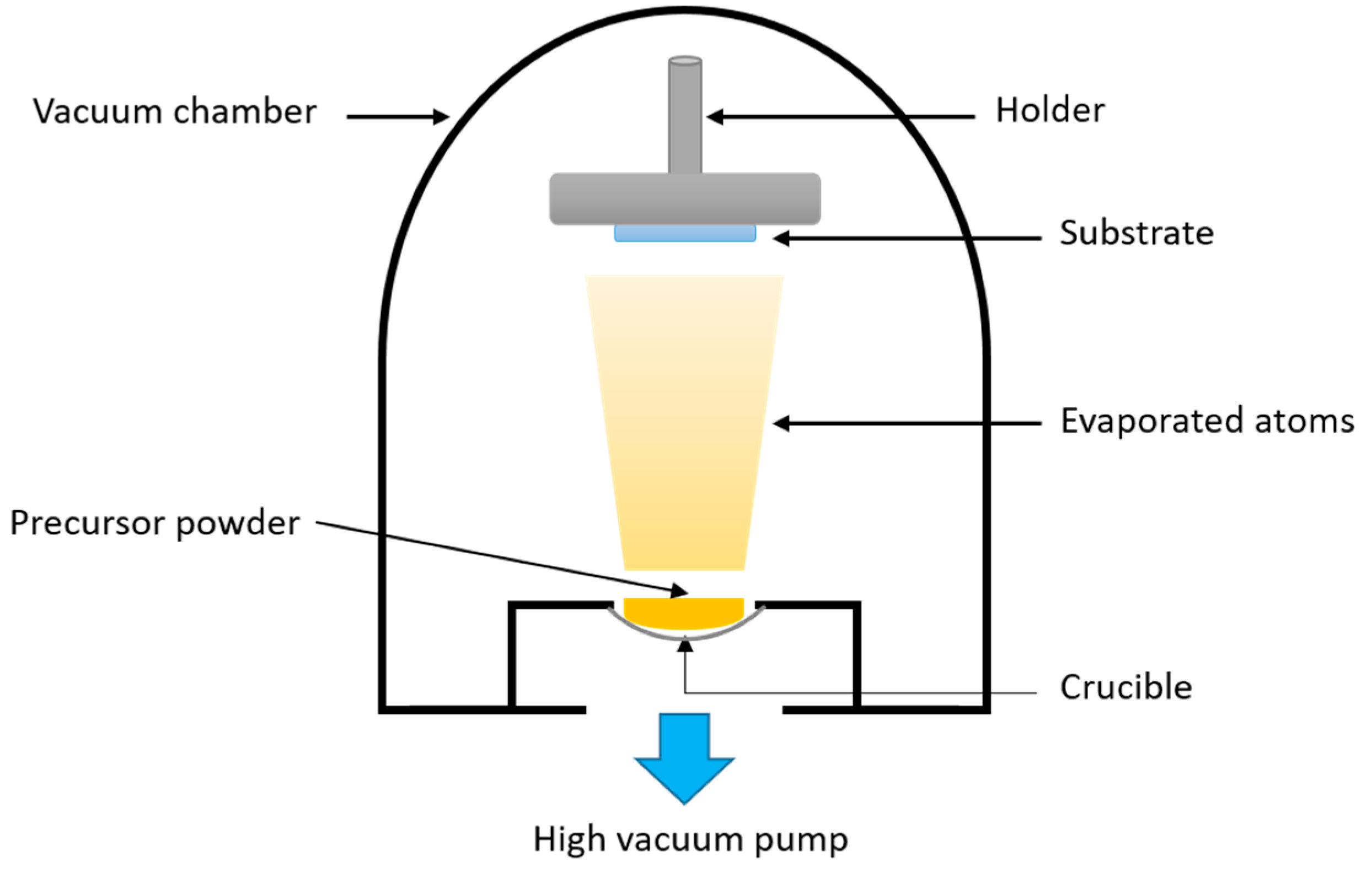
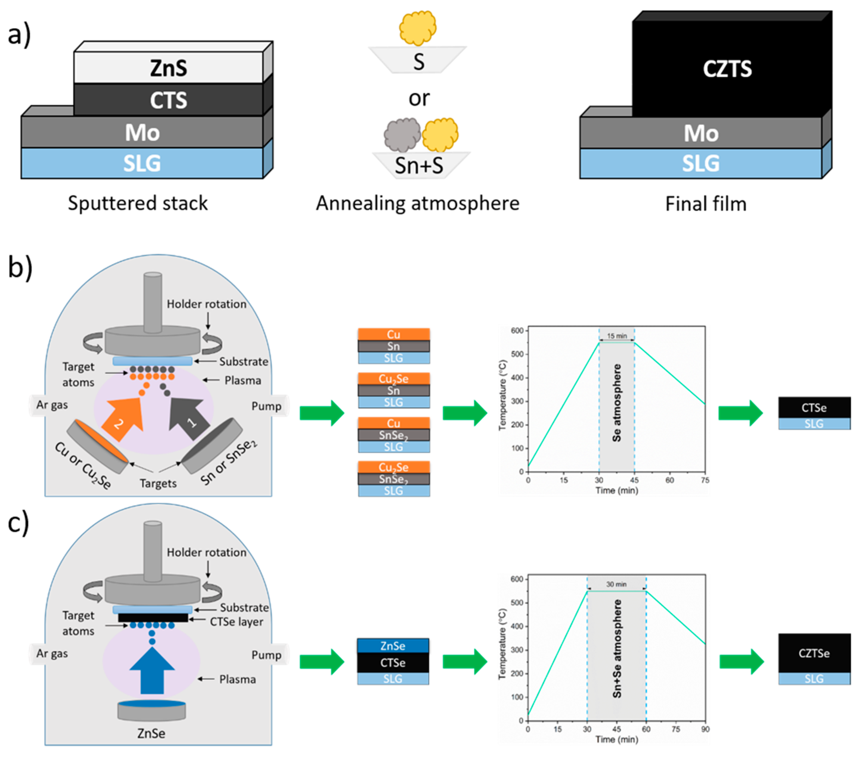
2.2.1. Evaporation
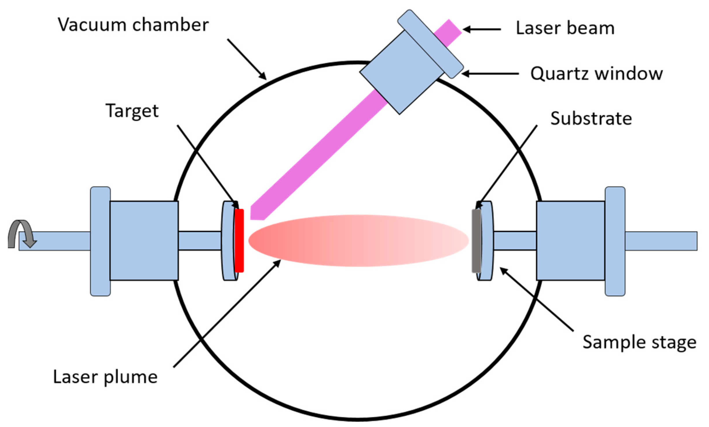
2.2.2. Pulsed Laser Deposition
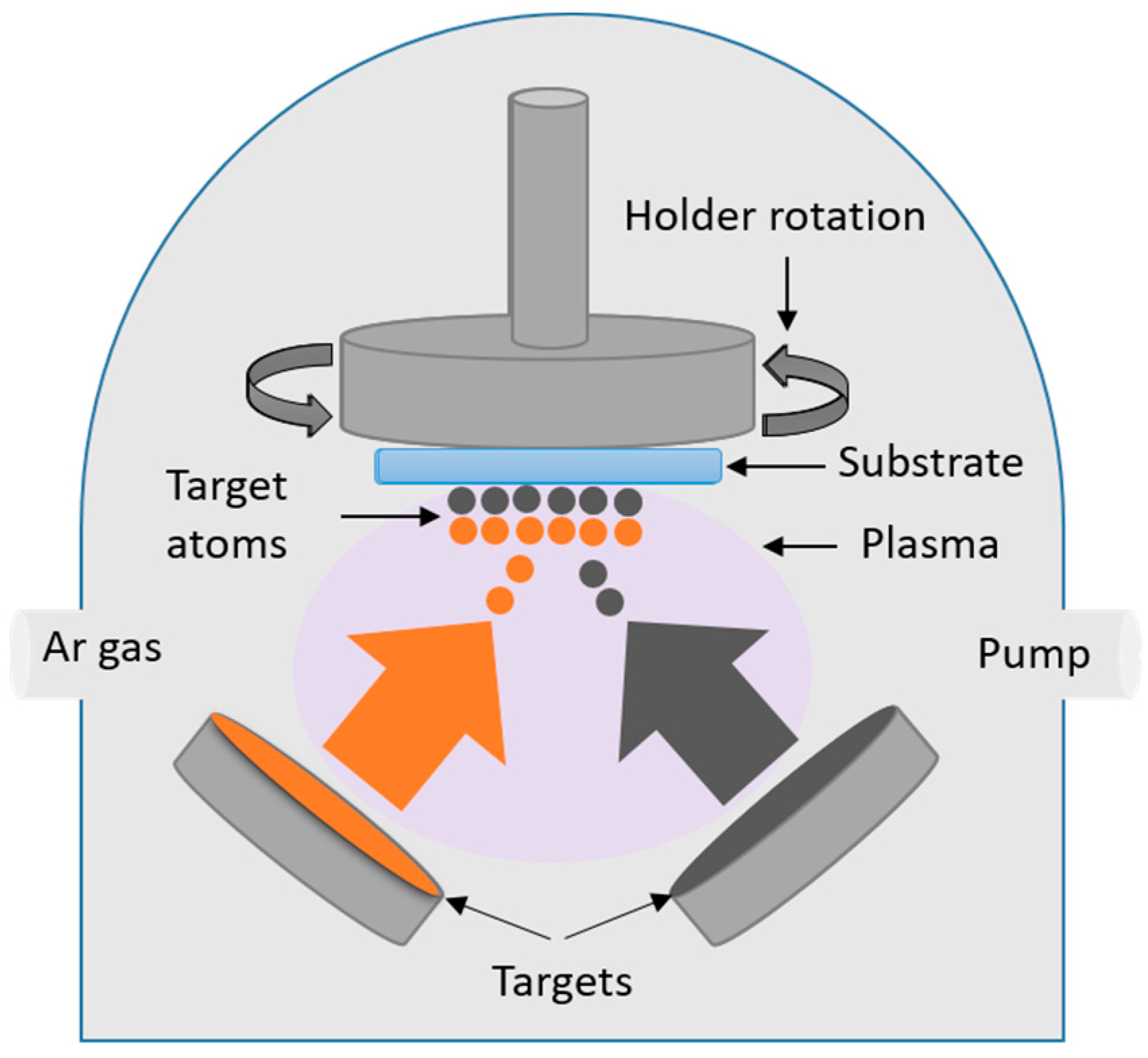
2.2.3. Magnetron Sputtering
3. Secondary Phases in CZT(S/Se)
3.1. Formation of Secondary Phases
3.2. Identification of Secondary Phases
3.2.1. Structural Analysis
X-ray Diffraction
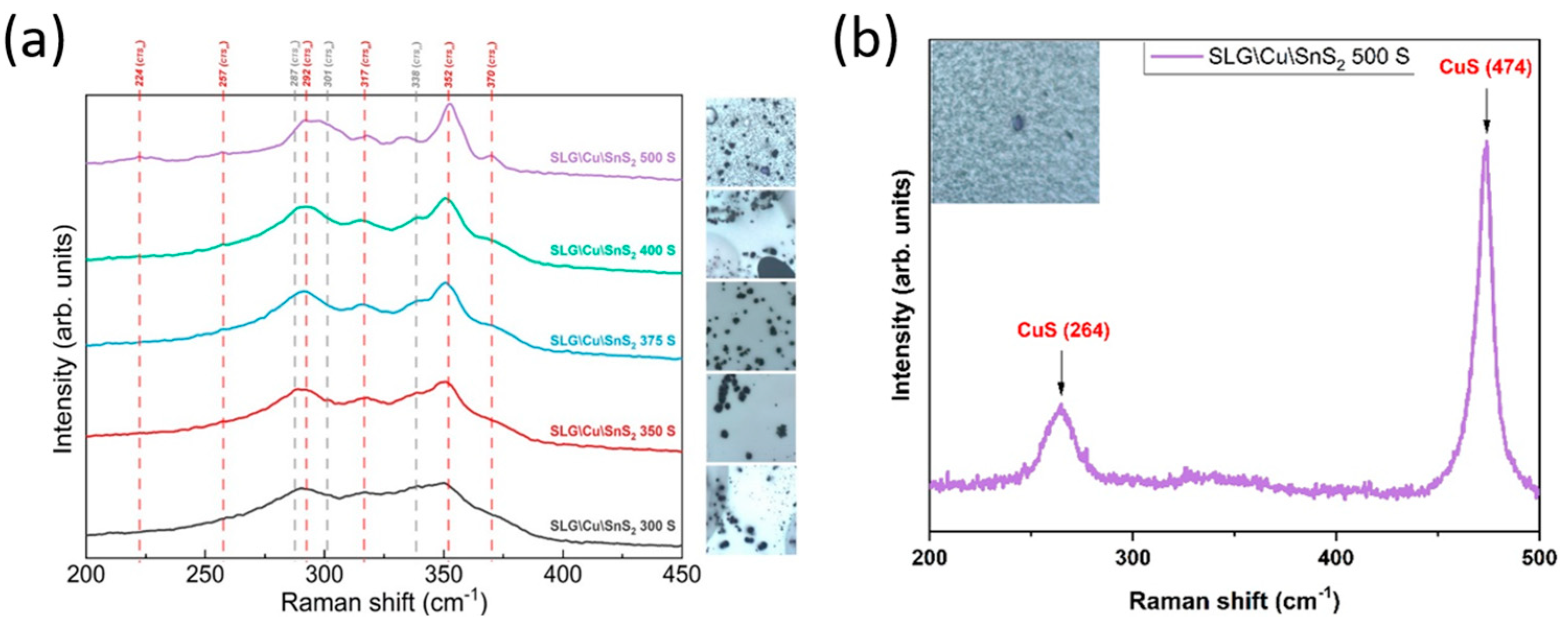
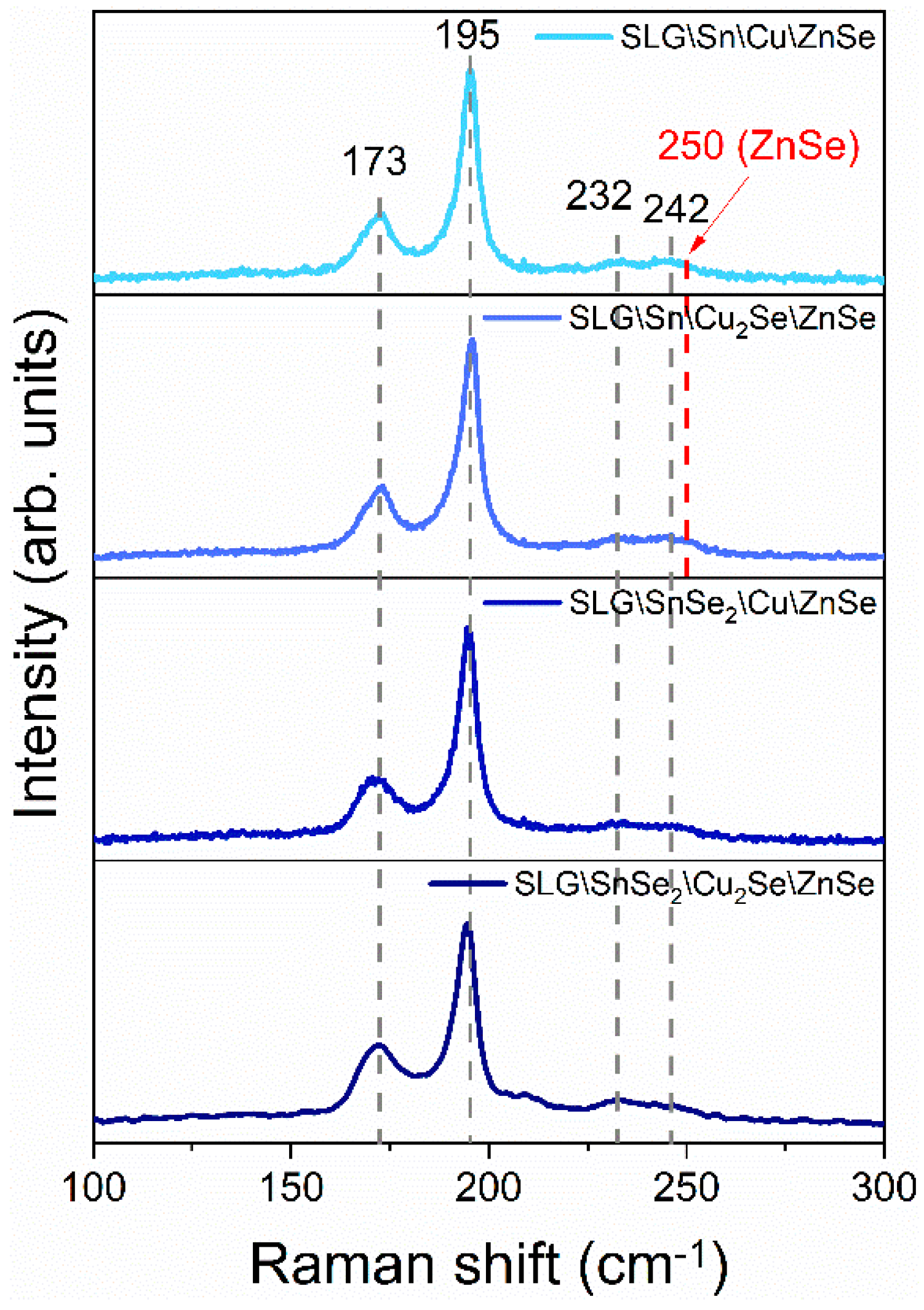
Raman Spectroscopy
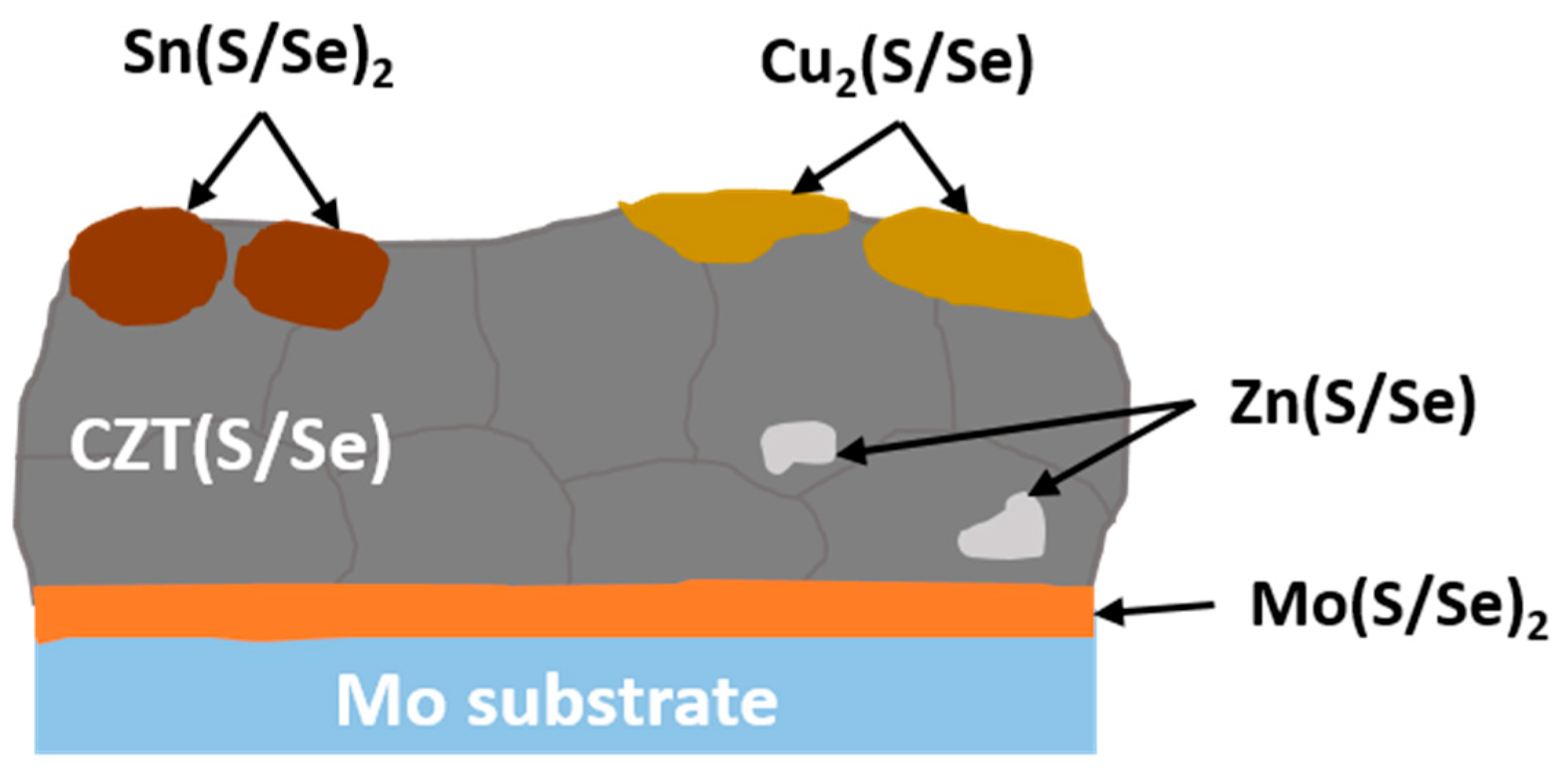
3.2.2. Morphological and Compositional Analysis
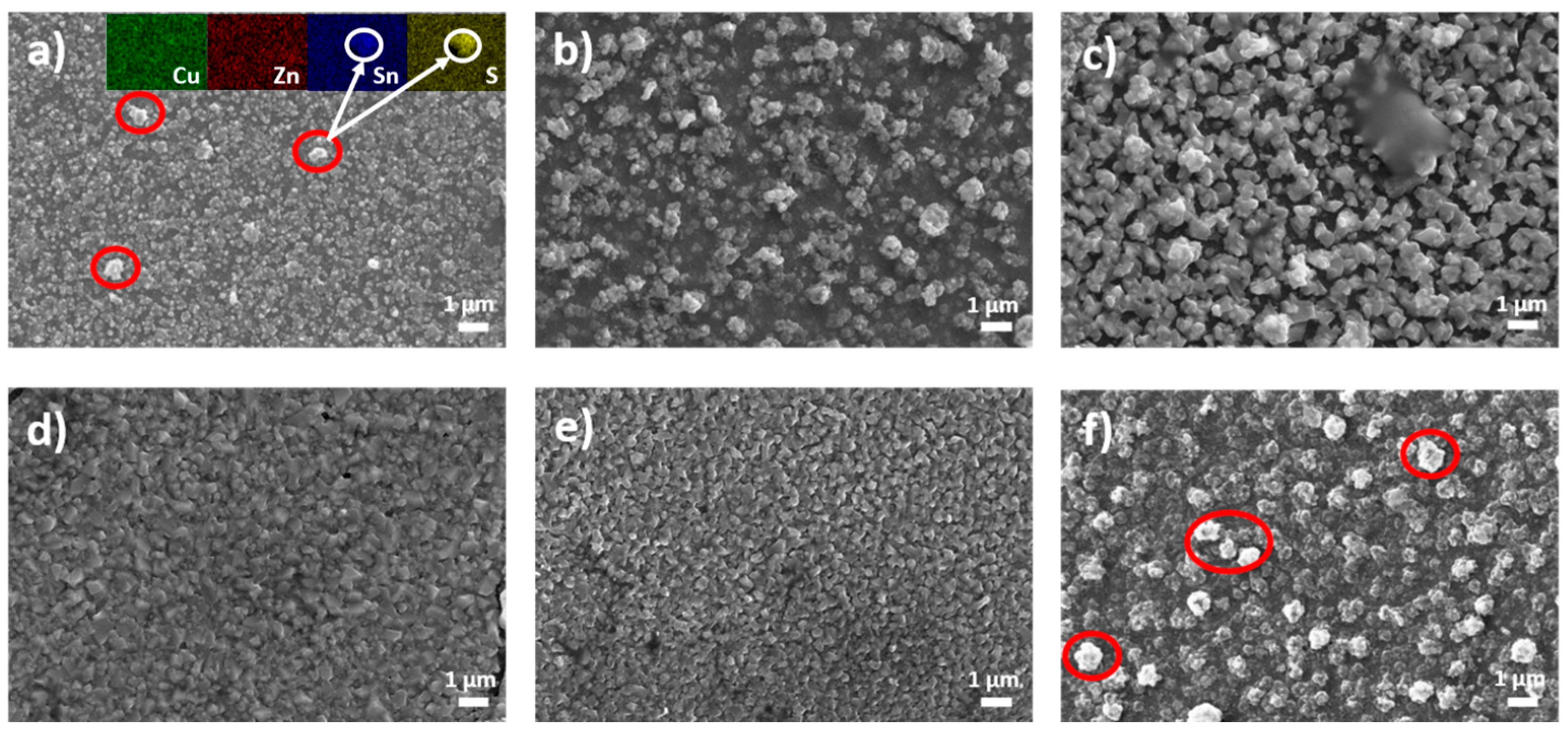
SEM-EDX
3.3. Strategies to Enhance Phase Control
4. Influence of Secondary Phases on the Solar Device Efficiency
5. Conclusions
Author Contributions
Funding
Data Availability Statement
Conflicts of Interest
References
- El Khouja, O.; Galca, A.C.; Nouneh, K.; Zaki, M.Y.; Ebn Touhami, M.; Taibi, M.; Matei, E.; Negrila, C.C.; Enculescu, M.; Pintilie, L. Structural, Morphological and Optical Properties of Cu–Fe–Sn–S Thin Films Prepared by Electrodeposition at Fixed Applied Potential. Thin Solid. Films 2021, 721, 138547. [Google Scholar] [CrossRef]
- Paul, S.; Gulyas, I.; Repins, I.L.; Mou, S.; Li, J.V. Carrier Transport Properties in a Thin-Film Cu2ZnSnSe4 Solar Cell. Thin Solid. Films 2019, 675, 103–108. [Google Scholar] [CrossRef]
- Zaki, M.-Y.; Sava, F.; Buruiana, A.-T.; Simandan, I.-D.; Becherescu, N.; Galca, A.-C.; Mihai, C.; Velea, A. Synthesis and Characterization of Cu2ZnSnS4 Thin Films Obtained by Combined Magnetron Sputtering and Pulsed Laser Deposition. Nanomaterials 2021, 11, 2403. [Google Scholar] [CrossRef] [PubMed]
- Padhy, S.; Mannu, R.; Singh, U.P. Graded Band Gap Structure of Kesterite Material Using Bilayer of CZTS and CZTSe for Enhanced Performance: A Numerical Approach. Solar Energy 2021, 216, 601–609. [Google Scholar] [CrossRef]
- Zaki, M.Y.; El Khouja, O.; Nouneh, K.; Ebn Touhami, M.; Matei, E.; Azmi, S.; Rusu, M.I.; Grigorescu, C.E.A.; Briche, S.; Boutamart, M.; et al. ZnS Stacking Order Influence on the Formation of Zn-Poor and Zn-Rich Cu2ZnSnS4 Phase. J. Mater. Sci Mater. Electron. 2022, 33, 11989–12001. [Google Scholar] [CrossRef]
- El Khouja, O.; Galca, A.C.; Zaki, M.Y.; Talbi, A.; Ahmoum, H.; Nouneh, K.; Ebn Touhami, M.; Taibi, M.; Matei, E.; Enculescu, M.; et al. Secondary Phases and Their Influence on Optical and Electrical Properties of Electrodeposited Cu2FeSnS4 Films. Appl. Phys. A 2021, 127, 887. [Google Scholar] [CrossRef]
- Zhang, Y.; Zhou, S.; Sun, K. Cu2ZnSnS4 (CZTS) for Photoelectrochemical CO2 Reduction: Efficiency, Selectivity, and Stability. Nanomaterials 2023, 13, 2762. [Google Scholar] [CrossRef] [PubMed]
- Khaaissa, Y.; Talbi, A.; Nouneh, K.; El Khouja, O.; Ahmoum, H.; Fahoume, M. Effect of Growth Temperature on the Physical Properties of Spray Pyrolysis Deposited CZTS Films. Mater. Today Proc. 2022, 66, 252–258. [Google Scholar] [CrossRef]
- Azmi, S.; Layachi, O.A.; Ouardi, M.E.; Khoumri, E.M.; Moujib, A.; Brouzi, A.E.; Nohair, M.; Pezzato, L.; Dabala, M. Growth of Cu2ZnSnS4 Thin Film Absorber Layer on Transparent Conductive Oxides and Molybdenum Substrates by Electrodeposition for Photovoltaic Application. Optik 2022, 250, 168320. [Google Scholar] [CrossRef]
- Hreid, T.; Li, J.; Zhang, Y.; Spratt, H.J.; Wang, H.; Will, G. Effects of Metal Ion Concentration on Electrodeposited CuZnSn Film and Its Application in Kesterite Cu2ZnSnS4 Solar Cells. RSC Adv. 2015, 5, 65114–65122. [Google Scholar] [CrossRef]
- Azmi, S.; Moujib, A.; Layachi, O.A.; Matei, E.; Galca, A.C.; Zaki, M.Y.; Secu, M.; Rusu, M.I.; Grigorescu, C.E.A.; Khoumri, E.M. Towards Phase Pure Kesterite Cu2ZnSnS4 Absorber Layers Growth via Single Step Free Sulfurization Electrodeposition under a Fix Applied Potential on Mo Substrate. J. Alloys Compd. 2020, 842, 155821. [Google Scholar] [CrossRef]
- Valdés, M.; Sánchez, Y.; Perelstein, G.; Oliva, F.; Izquierdo-Roca, V.; Rodriguez, A.P.; Saucedo, E. Influence of Co-Electrodeposition Parameters in the Synthesis of Kesterite Thin Films for Photovoltaic. J. Alloys Compd. 2020, 839, 155679. [Google Scholar] [CrossRef]
- Shafi, M.A.; Khan, L.; Ullah, S.; Bouich, A.; Ullah, H.; Mari, B. Synthesis of CZTS Kesterite by pH Adjustment in Order to Improve the Performance of CZTS Thin Film for Photovoltaic Applications. Micro Nanostruct. 2022, 164, 107185. [Google Scholar] [CrossRef]
- Pawar, B.S.; Pawar, S.M.; Shin, S.W.; Choi, D.S.; Park, C.J.; Kolekar, S.S.; Kim, J.H. Effect of Complexing Agent on the Properties of Electrochemically Deposited Cu2ZnSnS4 (CZTS) Thin Films. Appl. Surf. Sci. 2010, 257, 1786–1791. [Google Scholar] [CrossRef]
- Azmi, S.; Nohair, M.; El Marrakchi, M.; Khoumri, E.M.; Dabala, M. Effect of the Complexing Agents on the Properties of Electrodeposited CZTS Thin Films. In Proceedings of the 2018 7th International Conference on Renewable Energy Research and Applications (ICRERA), Paris, France, 14–17 October 2018; pp. 1346–1351. [Google Scholar]
- Zaki, M.Y.; Nouneh, K.; Touhami, M.E.; Matei, E.; Badica, P.; Burdusel, M.; Negrila, C.C.; Baibarac, M.; Pintilie, L.; Galca, A.C. Influence of Boric Acid Concentration on the Properties of Electrodeposited CZTS Absorber Layers. Phys. Scr. 2020, 95, 054001. [Google Scholar] [CrossRef]
- Ge, J.; Yan, Y. Controllable Multinary Alloy Electrodeposition for Thin-Film Solar Cell Fabrication: A Case Study of Kesterite Cu2ZnSnS4. iScience 2018, 1, 55–71. [Google Scholar] [CrossRef] [PubMed]
- Amrit, P.; Jain, S.; Tomar, M.; Gupta, V.; Joshi, B. Synthesis and Characterization of Sol Gel Derived Nontoxic CZTS Thin Films without Sulfurization. Int. J. Appl. Ceram. Technol. 2020, 17, 1194–1200. [Google Scholar] [CrossRef]
- Khushaim, M.; Alamri, S.; Kattan, N.; Jaber, A.; Alamri, S. Study of Kesterite Cu2ZnSnS4 (CZTS) Thin Films Deposited by Spray Technique for Photovoltaic Applications. J. Taibah Univ. Sci. 2021, 15, 329–339. [Google Scholar] [CrossRef]
- Ahmoum, H.; Chelvanathan, P.; Su’ait, M.S.; Boughrara, M.; Li, G.; Al-Waeli, A.H.A.; Sopian, K.; Kerouad, M.; Amin, N. Impact of Preheating Environment on Microstructural and Optoelectronic Properties of Cu2ZnSnS4 (CZTS) Thin Films Deposited by Spin-Coating. Superlattices Microstruct. 2020, 140, 106452. [Google Scholar] [CrossRef]
- Chaudhari, S.; Kannan, P.K.; Dey, S.R. Influence of Stabilizing Agent on Dip Coating of Cu2ZnSnS4 Thin Film. Thin Solid. Films 2017, 636, 144–149. [Google Scholar] [CrossRef]
- Ahmad, A.A.; Migdadi, A.B.; Alsaad, A.M.; Qattan, I.A.; Al-Bataineh, Q.M.; Telfah, A. Computational and Experimental Characterizations of Annealed Cu2ZnSnS4 Thin Films. Heliyon 2021, 8, e08683. [Google Scholar] [CrossRef]
- Shaikh, R.A.G.; More, S.A.; Bisen, G.G.; Ghosh, S.S. Study the Properties of Solution Processable CZTS Thin Films Induced by Annealing Treatment: Study of Annealing Time. Semiconductors 2020, 54, 1011–1015. [Google Scholar] [CrossRef]
- Aabel, P.; Anupama, A.; Kumar, M.C.S. Preparation and Characterization of CZTS Thin Films by Vacuum-Assisted Spray Pyrolysis and Fabrication of Cd-Free Heterojunction Solar Cells. Semicond. Sci. Technol. 2023, 38, 045010. [Google Scholar] [CrossRef]
- Diwate, K.; Mohite, K.; Shinde, M.; Rondiya, S.; Pawbake, A.; Date, A.; Pathan, H.; Jadkar, S. Synthesis and Characterization of Chemical Spray Pyrolysed CZTS Thin Films for Solar Cell Applications. Energy Procedia 2017, 110, 180–187. [Google Scholar] [CrossRef]
- Kumar, Y.B.K.; Babu, G.S.; Bhaskar, P.U.; Raja, V.S. Effect of Starting-solution pH on the Growth of Cu2ZnSnS4 Thin Films Deposited by Spray Pyrolysis. Physica Status Solidi 2009, 206, 1525–1530. [Google Scholar] [CrossRef]
- Shamardin, A.; Kurbatov, D.; Grase, L.; Vecstaudža, J.; Kaupužs, J.; Medvids, A. Quality Improvement of CZTS Thin Films Deposited by Spray Pyrolysis Method Using Pulsed Nd: YAG Laser Irradiation. Appl. Surf. Sci. 2019, 488, 827–835. [Google Scholar] [CrossRef]
- Kamoun, N.; Bouzouita, H.; Rezig, B. Fabrication and Characterization of Cu2ZnSnS4 Thin Films Deposited by Spray Pyrolysis Technique. Thin Solid. Films 2007, 515, 5949–5952. [Google Scholar] [CrossRef]
- Vauche, L.; Dubois, J.; Laparre, A.; Pasquinelli, M.; Bodnar, S.; Grand, P.-P.; Jaime, S. Rapid Thermal Processing Annealing Challenges for Large Scale Cu2ZnSnS4 Thin Films. Phys. Status Solidi A 2015, 212, 103–108. [Google Scholar] [CrossRef]
- Jung, S.; Gwak, J.; Yun, J.H.; Ahn, S.; Nam, D.; Cheong, H.; Ahn, S.; Cho, A.; Shin, K.; Yoon, K. Cu2ZnSnSe4 Thin Film Solar Cells Based on a Single-Step Co-Evaporation Process. Thin Solid. Films 2013, 535, 52–56. [Google Scholar] [CrossRef]
- Zhi, Z.; Wang, S.; Huang, L.; Li, J.; Xiao, X. Fabrication of CZTS Thin Films and Solar Cells via Single-Step Co-Evaporation Method. Mater. Sci. Semicond. Process. 2022, 144, 106592. [Google Scholar] [CrossRef]
- Zhang, L.; Karthikeyan, S.; Sibakoti, M.J.; Campbell, S.A. Cu2ZnSnS4 Thin Film Growth Optimization and Post Rapid Thermal Annealing of Solar Cells and Its Influence on Device Performance. In Proceedings of the 2015 IEEE 42nd Photovoltaic Specialist Conference (PVSC), New Orleans, LA, USA, 14–19 June 2015; pp. 1–6. [Google Scholar]
- Choudhari, N.J.; George, S.D.; Raviprakash, Y. Influence of Sulfurization Time and Cu-ZnS-Sn Stack Order on the Properties of Thermally Evaporated CZTS Thin Films. J. Mater. Sci: Mater. Electron. 2022, 33, 5341–5350. [Google Scholar] [CrossRef]
- Tao, S.; Dong, L.; Han, J.; Wang, Y.; Gong, Q.; Wei, J.; Zhao, M.; Zhuang, D. Efficiency Enhancement of CZTSe Solar Cells Based on in Situ K-Doped Precursor. J. Mater. Chem. A 2023, 11, 9085–9096. [Google Scholar] [CrossRef]
- Ogugua, S.N.; Ntwaeaborwa, O.M.; Swart, H.C. Latest Development on Pulsed Laser Deposited Thin Films for Advanced Luminescence Applications. Coatings 2020, 10, 1078. [Google Scholar] [CrossRef]
- Oulad Elhmaidi, Z.; Abd-Lefdil, M.; El Khakani, M.A. Photoconversion Optimization of Pulsed-Laser-Deposited p-CZTS/n-Si-Nanowires Heterojunction-Based Photovoltaic Devices. Nanomaterials 2020, 10, 1393. [Google Scholar] [CrossRef]
- Vanalakar, S.A.; Agawane, G.L.; Shin, S.W.; Suryawanshi, M.P.; Gurav, K.V.; Jeon, K.S.; Patil, P.S.; Jeong, C.W.; Kim, J.Y.; Kim, J.H. A Review on Pulsed Laser Deposited CZTS Thin Films for Solar Cell Applications. J. Alloys Compd. 2015, 619, 109–121. [Google Scholar] [CrossRef]
- Cazzaniga, A.; Crovetto, A.; Yan, C.; Sun, K.; Hao, X.; Ramis Estelrich, J.; Canulescu, S.; Stamate, E.; Pryds, N.; Hansen, O.; et al. Ultra-Thin Cu2ZnSnS4 Solar Cell by Pulsed Laser Deposition. Sol. Energy Mater. Sol. Cells 2017, 166, 91–99. [Google Scholar] [CrossRef]
- Ettlinger, R.B.; Crovetto, A.; Canulescu, S.; Cazzaniga, A.; Ravnkilde, L.; Youngman, T.; Hansen, O.; Pryds, N.; Schou, J. Formation of Copper Tin Sulfide Films by Pulsed Laser Deposition at 248 and 355 Nm. Appl. Phys. A 2016, 122, 466. [Google Scholar] [CrossRef]
- Cazzaniga, A.; Ettlinger, R.B.; Canulescu, S.; Schou, J.; Pryds, N. Nanosecond Laser Ablation and Deposition of Silver, Copper, Zinc and Tin. Appl. Phys. A 2014, 117, 89–92. [Google Scholar] [CrossRef]
- Noroozi, M.; Petruhins, A.; Greczynski, G.; Rosen, J.; Eklund, P. Structural and Mechanical Properties of Amorphous AlMgB14 Thin Films Deposited by DC Magnetron Sputtering on Si, Al2O3 and MgO Substrates. Appl. Phys. A 2020, 126, 133. [Google Scholar] [CrossRef]
- Olgar, M.A.; Klaer, J.; Mainz, R.; Levcenco, S.; Just, J.; Bacaksiz, E.; Unold, T. Effect of Precursor Stacking Order and Sulfurization Temperature on Compositional Homogeneity of CZTS Thin Films. Thin Solid. Films 2016, 615, 402–408. [Google Scholar] [CrossRef]
- Jheng, B.-T.; Liu, P.-T.; Wu, M.-C. A Promising Sputtering Route for Dense Cu2ZnSnS4 Absorber Films and Their Photovoltaic Performance. Sol. Energy Mater. Sol. Cells 2014, 128, 275–282. [Google Scholar] [CrossRef]
- Xie, M.; Zhuang, D.; Zhao, M.; Zhuang, Z.; Ouyang, L.; Li, X.; Song, J. Preparation and Characterization of Cu2ZnSnS4 Thin Films and Solar Cells Fabricated from Quaternary Cu-Zn-Sn-S Target. Int. J. Photoenergy 2013, 2013, 1–9. [Google Scholar] [CrossRef]
- Olgar, M.A.; Klaer, J.; Mainz, R.; Ozyuzer, L.; Unold, T. Cu2ZnSnS4-Based Thin Films and Solar Cells by Rapid Thermal Annealing Processing. Thin Solid. Films 2017, 628, 1–6. [Google Scholar] [CrossRef]
- Behera, N.; Mohan, D.B. The Phase Optimization, Optical and Electrical Properties of Kesterite Cu2ZnSnS4 Thin Film Prepared by Single Target RF Magnetron Sputtering Technique for Solar Cell Application. Mater. Res. Express 2020, 6, 126457. [Google Scholar] [CrossRef]
- Zhao, L.; Fei, F.Y.; Wang, J.; Wang, F.; Wang, C.; Li, J.; Wang, J.; Cheng, Z.; Dou, S.; Wang, X. Improvement of Thermoelectric Properties and Their Correlations with Electron Effective Mass in Cu1.98SxSe1−x. Sci. Rep. 2017, 7, 40436. [Google Scholar] [CrossRef]
- Khalkar, A.; Lim, K.-S.; Yu, S.-M.; Patole, S.P.; Yoo, J.-B. Deposition of Cu2ZnSnS4 Thin Films by Magnetron Sputtering and Subsequent Sulphurization. Electron. Mater. Lett. 2014, 10, 43–49. [Google Scholar] [CrossRef]
- Gudmundsson, J.T. Physics and Technology of Magnetron Sputtering Discharges. Plasma Sources Sci. Technol. 2020, 29, 113001. [Google Scholar] [CrossRef]
- Alvarez, R.; Garcia-Valenzuela, A.; Lopez-Santos, C.; Ferrer, F.J.; Rico, V.; Guillen, E.; Alcon-Camas, M.; Escobar-Galindo, R.; Gonzalez-Elipe, A.R.; Palmero, A. High-Rate Deposition of Stoichiometric Compounds by Reactive Magnetron Sputtering at Oblique Angles. Plasma Process. Polym. 2016, 13, 960–964. [Google Scholar] [CrossRef]
- Vishwakarma, M.; Karakulina, O.M.; Abakumov, A.M.; Hadermann, J.; Mehta, B.R. Nanoscale Characterization of Growth of Secondary Phases in Off-Stoichiometric CZTS Thin Films. J. Nanosci. Nanotechnol. 2018, 18, 1688–1695. [Google Scholar] [CrossRef]
- Sava, F.; Diagne, O.; Galca, A.-C.; Simandan, I.-D.; Matei, E.; Burdusel, M.; Becherescu, N.; Becherescu, V.; Mihai, C.; Velea, A. Secondary Crystalline Phases Influence on Optical Properties in Off-Stoichiometric Cu2S–ZnS–SnS2 Thin Films. Materials 2020, 13, 4624. [Google Scholar] [CrossRef]
- Hartman, K.; Newman, B.K.; Johnson, J.L.; Du, H.; Fernandes, P.A.; Chawla, V.; Bolin, T.; Clemens, B.M.; Da Cunha, A.F.; Teeter, G.; et al. Detection of ZnS Phases in CZTS Thin-Films by EXAFS. In Proceedings of the 2011 37th IEEE Photovoltaic Specialists Conference, Seattle, WA, USA, 19–24 June 2011; pp. 2506–2509. [Google Scholar]
- Agrawal, S.; De Souza, D.O.; Balasubramanian, C.; Mukherjee, S. Effect of Secondary Phases Controlled by Precursor Composition on the Efficiency of CZTS Thin Film Solar Cell. Sol. Energy Mater. Sol. Cells 2024, 267, 112719. [Google Scholar] [CrossRef]
- Raiguru, J.; Subramanyam, B.; Sa, K.; Alam, I.; Das, S.; Mukherjee, J.; Mahakul, P.C.; Subudhi, B.; Mahanandia, P. Impact of Annealing Temperature on the Phase of CZTS with the Variation in Surface Morphological Changes and Extraction of Optical Bandgap. IOP Conf. Ser. Mater. Sci. Eng. 2017, 178, 012017. [Google Scholar] [CrossRef]
- Ashfaq, A.; Jacob, J.; Bano, N.; Nabi, M.A.U.; Ali, A.; Ahmad, W.; Mahmood, K.; Arshad, M.I.; Ikram, S.; Rehman, U.; et al. A Two Step Technique to Remove the Secondary Phases in CZTS Thin Films Grown by Sol-Gel Method. Ceram. Int. 2019, 45, 10876–10881. [Google Scholar] [CrossRef]
- Chen, G.; Wang, W.; Zhang, J.; Chen, S.; Huang, Z. Formation Mechanism of Secondary Phases in Cu2ZnSnS4 Growth under Different Copper Content. Mater. Lett. 2017, 186, 98–101. [Google Scholar] [CrossRef]
- Stanchik, A.V.; Tivanov, M.S.; Tyukhov, I.I.; Juskenas, R.; Korolik, O.V.; Gremenok, V.F.; Saad, A.M.; Naujokaitis, A. Temperature Dependence of Raman Scattering in the Cu2ZnSnSe4 Thin Films on a Ta Foil Substrate. Sol. Energy 2020, 201, 480–488. [Google Scholar] [CrossRef]
- Vishwakarma, M.; Agrawal, K.; Hadermann, J.; Mehta, B.R. Investigating the Effect of Sulphurization on Volatility of Compositions in Cu-Poor and Sn-Rich CZTS Thin Films. Appl. Surf. Sci. 2020, 507, 145043. [Google Scholar] [CrossRef]
- Redinger, A.; Hönes, K.; Fontané, X.; Izquierdo-Roca, V.; Saucedo, E.; Valle, N.; Pérez-Rodríguez, A.; Siebentritt, S. Detection of a ZnSe Secondary Phase in Coevaporated Cu2ZnSnSe4 Thin Films. Appl. Phys. Lett. 2011, 98, 101907. [Google Scholar] [CrossRef]
- Ghediya, P.R.; Chaudhuri, T.K. Microwave-Processed Copper Zinc Tin Sulphide (CZTS) Inks for Coatings in Solar Cells. In Advanced Ceramic and Metallic Coating and Thin Film Materials for Energy and Environmental Applications; Zhang, J., Jung, Y.-G., Eds.; Springer International Publishing: Cham, Switzerland, 2018; pp. 121–174. ISBN 978-3-319-59905-2. [Google Scholar]
- Jiang, M.; Yan, X. Cu2ZnSnS4 Thin Film Solar Cells: Present Status and Future Prospects. In Solar Cells-Research and Application Perspectives; Morales-Acevedo, A., Ed.; InTech: Rijeka, Croatia, 2013; ISBN 978-953-51-1003-3. [Google Scholar]
- Shi, Z.; Attygalle, D.; Jayatissa, A.H. Kesterite-Based next Generation High Performance Thin Film Solar Cell: Current Progress and Future Prospects. J. Mater. Sci. Mater. Electron. 2017, 28, 2290–2306. [Google Scholar] [CrossRef]
- Berg, D.M.; Arasimowicz, M.; Djemour, R.; Gütay, L.; Siebentritt, S.; Schorr, S.; Fontané, X.; Izquierdo-Roca, V.; Pérez-Rodriguez, A.; Dale, P.J. Discrimination and Detection Limits of Secondary Phases in Cu2ZnSnS4 Using X-Ray Diffraction and Raman Spectroscopy. Thin Solid. Films 2014, 569, 113–123. [Google Scholar] [CrossRef]
- Zaki, M.Y.; Sava, F.; Simandan, I.-D.; Buruiana, A.T.; Stavarache, I.; Bocirnea, A.E.; Mihai, C.; Velea, A.; Galca, A.-C. A Two-Step Magnetron Sputtering Approach for the Synthesis of Cu2ZnSnS4 Films from Cu2SnS3\ZnS Stacks. ACS Omega 2022, 7, 23800–23814. [Google Scholar] [CrossRef]
- Tanaka, T.; Sueishi, T.; Saito, K.; Guo, Q.; Nishio, M.; Yu, K.M.; Walukiewicz, W. Existence and Removal of Cu2Se Second Phase in Coevaporated Cu2ZnSnSe4 Thin Films. J. Appl. Phys. 2012, 111, 053522. [Google Scholar] [CrossRef]
- Zaki, M.Y.; Sava, F.; Simandan, I.D.; Buruiana, A.T.; Mihai, C.; Velea, A.; Galca, A.C. Cu2SnSe3 Phase Formation from Different Metallic and Binary Chalcogenides Stacks Using Magnetron Sputtering. Mater. Sci. Semicond. Process. 2023, 153, 107195. [Google Scholar] [CrossRef]
- Salomé, P.M.P.; Fernandes, P.A.; Leitão, J.P.; Sousa, M.G.; Teixeira, J.P.; da Cunha, A.F. Secondary Crystalline Phases Identification in Cu2ZnSnSe4 Thin Films: Contributions from Raman Scattering and Photoluminescence. J. Mater. Sci. 2014, 49, 7425–7436. [Google Scholar] [CrossRef]
- Catana, D.-S.; Zaki, M.Y.; Simandan, I.-D.; Buruiana, A.-T.; Sava, F.; Velea, A. Understanding the Effects of Post-Deposition Sequential Annealing on the Physical and Chemical Properties of Cu2ZnSnSe4 Thin Films. Surfaces 2023, 6, 466–479. [Google Scholar] [CrossRef]
- Dimitrievska, M.; Xie, H.; Fairbrother, A.; Fontané, X.; Gurieva, G.; Saucedo, E.; Pérez-Rodríguez, A.; Schorr, S.; Izquierdo-Roca, V. Multiwavelength Excitation Raman Scattering of Cu2ZnSn(SxSe1−x)4 (0 ≤ x ≤ 1) Polycrystalline Thin Films: Vibrational Properties of Sulfoselenide Solid Solutions. Appl. Phys. Lett. 2014, 105, 031913. [Google Scholar] [CrossRef]
- Dimitrievska, M.; Boero, F.; Litvinchuk, A.P.; Delsante, S.; Borzone, G.; Perez-Rodriguez, A.; Izquierdo-Roca, V. Structural Polymorphism in “Kesterite” Cu2ZnSnS4: Raman Spectroscopy and First-Principles Calculations Analysis. Inorg. Chem. 2017, 56, 3467–3474. [Google Scholar] [CrossRef]
- Fernandes, P.A.; Salomé, P.M.P.; da Cunha, A.F. A Study of Ternary Cu2SnS3 and Cu3SnS4 Thin Films Prepared by Sulfurizing Stacked Metal Precursors. J. Phys. D Appl. Phys. 2010, 43, 215403. [Google Scholar] [CrossRef]
- Avellaneda, D.; Paul, A.; Shaji, S.; Krishnan, B. Synthesis of Cu2SnS3, Cu3SnS4, and Cu4SnS4 Thin Films by Sulfurization of SnS-Cu Layers at a Selected Temperature and /or Cu Layers Thickness. J. Solid. State Chem. 2022, 306, 122711. [Google Scholar] [CrossRef]
- Gang, M.G.; Gurav, K.V.; Shin, S.W.; Hong, C.W.; Min, J.H.; Suryawanshi, M.P.; Vanalakar, S.A.; Lee, D.S.; Kim, J.H. A 5.1% Efficient Kesterite Cu2ZnSnS4 (CZTS) Thin Film Solar Cell Prepared Using Modified Sulfurization Process. Phys. Status Solidi (C) Curr. Top. Solid. State Phys. 2015, 12, 713–716. [Google Scholar] [CrossRef]
- Patel, K.; Kheraj, V.; Shah, D.V.; Panchal, C.J.; Dhere, N.G. Cu2ZnSnS4 Thin-Films Grown by Dip-Coating: Effects of Annealing. J. Alloys Compd. 2016, 663, 842–847. [Google Scholar] [CrossRef]
- Zaki, M.Y.; Sava, F.; Simandan, I.D.; Buruiana, A.T.; Mihai, C.; Velea, A.; Galca, A.C. Effect of the Stacking Order, Annealing Temperature and Atmosphere on Crystal Phase and Optical Properties of Cu2SnS3. Sci. Rep. 2022, 12, 7958. [Google Scholar] [CrossRef]
- Tian, G.; Huang, C.; Luo, X.; Zhao, Z.; Peng, Y.; Gao, Y.; Tang, N.; Dsoke, S. Study of the Lithium Storage Mechanism of N-Doped Carbon-Modified Cu2S Electrodes for Lithium-Ion Batteries. Chem. A Eur. J. 2021, 27, 13774–13782. [Google Scholar] [CrossRef]
- Lund, E.A.; Du, H.; Hlaing OO, W.M.; Teeter, G.; Scarpulla, M.A. Investigation of Combinatorial Coevaporated Thin Film Cu2ZnSnS4 (II): Beneficial Cation Arrangement in Cu-Rich Growth. J. Appl. Phys. 2014, 115, 173503. [Google Scholar] [CrossRef]
- Gong, X.; Yan, T.; Li, J.; Liu, J.; Zou, H.; Zhang, B.; Wu, H.; Zhou, Z.; Zhou, X. Revealing the Anisotropic Phonon Behaviours of Layered SnS by Angle/Temperature-Dependent Raman Spectroscopy. RSC Adv. 2022, 12, 32262–32269. [Google Scholar] [CrossRef]
- Raadik, T.; Grossberg, M.; Krustok, J.; Kauk-Kuusik, M.; Crovetto, A.; Bolt Ettlinger, R.; Hansen, O.; Schou, J. Temperature Dependent Photoreflectance Study of Cu2SnS3 Thin Films Produced by Pulsed Laser Deposition. Appl. Phys. Lett. 2017, 110, 261105. [Google Scholar] [CrossRef]
- Ahmet, I.Y.; Hill, M.S.; Johnson, A.L.; Peter, L.M. Polymorph-Selective Deposition of High Purity SnS Thin Films from a Single Source Precursor. Chem. Mater. 2015, 27, 7680–7688. [Google Scholar] [CrossRef]
- Skelton, J.M.; Burton, L.A.; Jackson, A.J.; Oba, F.; Parker, S.C.; Walsh, A. Lattice Dynamics of the Tin Sulphides SnS2, SnS and Sn2S3: Vibrational Spectra and Thermal Transport. Phys. Chem. Chem. Phys. 2017, 19, 12452–12465. [Google Scholar] [CrossRef]
- Zhang, K.; Su, Z.; Zhao, L.; Yan, C.; Liu, F.; Cui, H.; Hao, X.; Liu, Y. Improving the Conversion Efficiency of Cu2ZnSnS4 Solar Cell by Low Pressure Sulfurization. Appl. Phys. Lett. 2014, 104, 141101. [Google Scholar] [CrossRef]
- Alvarez Barragan, A.; Malekpour, H.; Exarhos, S.; Balandin, A.A.; Mangolini, L. Grain-to-Grain Compositional Variations and Phase Segregation in Copper–Zinc–Tin–Sulfide Films. ACS Appl. Mater. Interfaces 2016, 8, 22971–22976. [Google Scholar] [CrossRef]
- Babichuk, I.S.; Semenenko, M.O.; Caballero, R.; Datsenko, O.I.; Golovynskyi, S.; Qiu, R.; Huang, C.; Hu, R.; Babichuk, I.V.; Ziniuk, R.R.; et al. Raman Mapping of MoS2 at Cu2ZnSnS4/Mo Interface in Thin Film. Sol. Energy 2020, 205, 154–160. [Google Scholar] [CrossRef]
- Huang, S.; Liang, L.; Ling, X.; Puretzky, A.A.; Geohegan, D.B.; Sumpter, B.G.; Kong, J.; Meunier, V.; Dresselhaus, M.S. Low-Frequency Interlayer Raman Modes to Probe Interface of Twisted Bilayer MoS2. Nano Lett. 2016, 16, 1435–1444. [Google Scholar] [CrossRef] [PubMed]
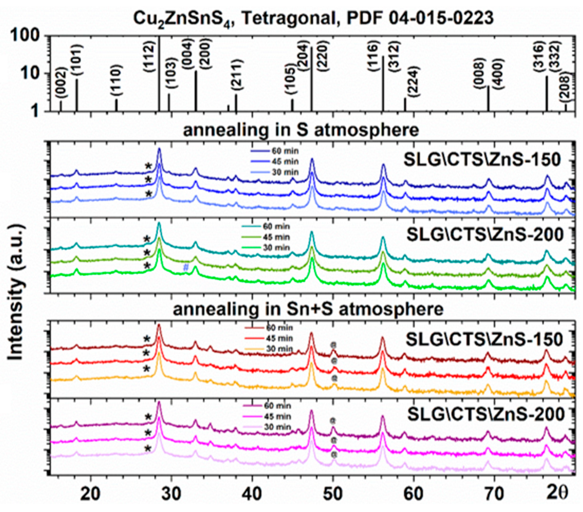
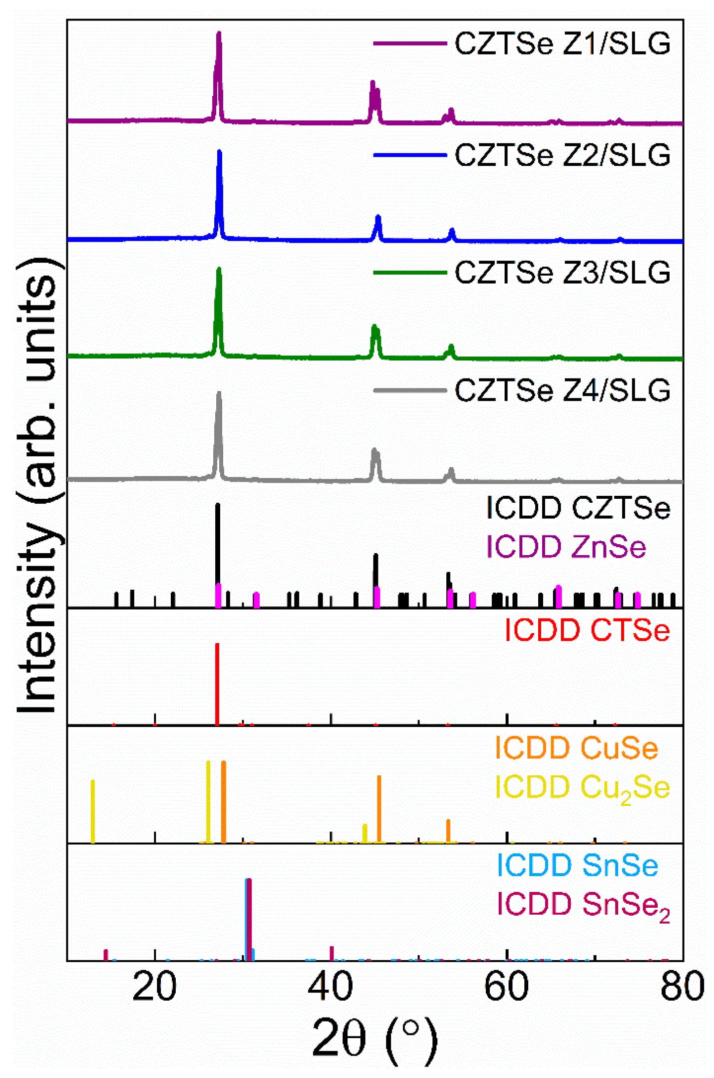
- Zaki, M.Y.; Sava, F.; Simandan, I.D.; Buruiana, A.T.; Bocirnea, A.E.; Stavarache, I.; Velea, A.; Galca, A.C.; Pintilie, L. From Non-Stoichiometric CTSe to Single Phase and Stoichiometric CZTSe Films by Annealing under Sn+Se Atmosphere. Ceram. Int. 2023, 49, 33692–33702. [Google Scholar] [CrossRef]
- Dimitrievska, M.; Oliva, F.; Guc, M.; Giraldo, S.; Saucedo, E.; Pérez-Rodríguez, A.; Izquierdo-Roca, V. Defect Characterisation in Cu2ZnSnSe4 Kesterites via Resonance Raman Spectroscopy and the Impact on Optoelectronic Solar Cell Properties. J. Mater. Chem. A 2019, 7, 13293–13304. [Google Scholar] [CrossRef]
- Ahmadi, M.; Pramana, S.S.; Batabyal, S.K.; Boothroyd, C.; Mhaisalkar, S.G.; Lam, Y.M. Synthesis of Cu2SnSe3 Nanocrystals for Solution Processable Photovoltaic Cells. Inorg. Chem. 2013, 52, 1722–1728. [Google Scholar] [CrossRef] [PubMed]
- Altosaar, M.; Raudoja, J.; Timmo, K.; Danilson, M.; Grossberg, M.; Krustok, J.; Mellikov, E. Cu2Zn1–x CdxSn(Se1–ySy)4 Solid Solutions as Absorber Materials for Solar Cells. Phys. Status Solidi 2008, 205, 167–170. [Google Scholar] [CrossRef]
- Shitu, I.G.; Liew, J.Y.C.; Talib, Z.A.; Baqiah, H.; Awang Kechik, M.M.; Ahmad Kamarudin, M.; Osman, N.H.; Low, Y.J.; Lakin, I.I. Influence of Irradiation Time on the Structural and Optical Characteristics of CuSe Nanoparticles Synthesized via Microwave-Assisted Technique. ACS Omega 2021, 6, 10698–10708. [Google Scholar] [CrossRef] [PubMed]
- Juškėnas, R.; Mockus, Z.; Giraitis, R.; Selskis, A.; Stalnionis, G.; Kanapeckaitė, S.; Drabavičius, A.; Kalinauskas, P.; Niaura, G. Structural and Photoelectrochemical Characterization of Cu2SnSe3 Thin Films Fabricated by Electrochemical Co-Deposition and Selenization. J. Alloys Compd. 2018, 767, 345–352. [Google Scholar] [CrossRef]
- Gurieva, G.; Levcenco, S.; Pereira Correia de Sousa, A.; Unold, T.; Schorr, S. Investigation of Detection Limits of ZnSe and Cu2SnSe3 Secondary Phases in Cu2ZnSnSe4. Phys. Status Solidi C 2017, 14, 1700166. [Google Scholar]
- Nam, D.; Lee, J.-U.; Cheong, H. Excitation Energy Dependent Raman Spectrum of MoSe2. Sci. Rep. 2015, 5, 17113. [Google Scholar] [CrossRef]
- Ismail, A.; Cho, J.W.; Park, S.J.; Hwang, Y.J.; Min, B.K. Synthesis of Solution-Processed Cu2ZnSnSe4 Thin Films on Transparent Conducting Oxide Glass Substrates. Bull. Korean Chem. Soc. 2014, 35, 1985–1988. [Google Scholar] [CrossRef]
- Just, J.; Sutter-Fella, C.M.; Lützenkirchen-Hecht, D.; Frahm, R.; Schorr, S.; Unold, T. Secondary Phases and Their Influence on the Composition of the Kesterite Phase in CZTS and CZTSe Thin Films. Phys. Chem. Chem. Phys. 2016, 18, 15988–15994. [Google Scholar] [CrossRef] [PubMed]
- Rudisch, K.; Davydova, A.; Riekehr, L.; Adolfsson, J.; Quaglia Casal, L.; Platzer-Björkman, C.; Scragg, J. Prospects for Defect Engineering in Cu2ZnSnS4 Solar Absorber Films. J. Mater. Chem. A 2020, 8, 15864–15874. [Google Scholar] [CrossRef]
- Abusnina, M.; Matin, M.; Moutinho, H.R.; Blackburn, J.L.; Alleman, J.; DeHart, C.; To, B.; Al-Jassim, M. Suppression of the Cu2−xS Secondary Phases in CZTS Films Through Controlling the Film Elemental Composition. IEEE J. Photovolt. 2015, 5, 1470–1475. [Google Scholar] [CrossRef]
- Kalinauskas, P.; Norkus, E.; Mockus, Z.; Giraitis, R.; Stalnionis, G.; Jasulaitiene, V.; Juškėnas, R. The Influence of Removal of Secondary Phases and Dissolution By-Product from the Surface of Cu2ZnSnS4 Film on the Photoelectrochemical Response of This Film. J. Electrochem. Soc. 2020, 167, 026513. [Google Scholar] [CrossRef]
- Yu, S.M.; Lim, K.-S.; Shin, D.-W.; Oh, T.-S.; Yoo, J.-B. Effect of the Intermediate Sulfide Layer on the Cu2ZnSnS4-Based Solar Cells. J. Mater. Sci: Mater. Electron. 2017, 28, 5696–5702. [Google Scholar] [CrossRef]
- Li, W.; Chen, J.; Yan, C.; Liu, F.; Hao, X. Transmission Electron Microscopy Analysis for the Process of Crystallization of Cu2ZnSnS4 Film from Sputtered Zn/CuSn Precursor. Nanotechnology 2014, 25, 195701. [Google Scholar] [CrossRef] [PubMed]
- Buffière, M.; Brammertz, G.; Batuk, M.; Verbist, C.; Mangin, D.; Koble, C.; Hadermann, J.; Meuris, M.; Poortmans, J. Microstructural Analysis of 9.7% Efficient Cu2ZnSnSe4 Thin Film Solar Cells. Appl. Phys. Lett. 2014, 105, 183903. [Google Scholar] [CrossRef]
- Fella, C.M.; Uhl, A.R.; Romanyuk, Y.E.; Tiwari, A.N. Cu2ZnSnSe4 Absorbers Processed from Solution Deposited Metal Salt Precursors under Different Selenization Conditions. Physica Status Solidi 2012, 209, 1043–1048. [Google Scholar] [CrossRef]
- Scragg, J.J.; Kubart, T.; Wätjen, J.T.; Ericson, T.; Linnarsson, M.K.; Platzer-Björkman, C. Effects of Back Contact Instability on Cu2ZnSnS4 Devices and Processes. Chem. Mater. 2013, 25, 3162–3171. [Google Scholar] [CrossRef]
- Bishop, D.M.; McCandless, B.E.; Mangan, T.C.; Dobson, K.; Birkmire, R. Effects of Growth Conditions on Secondary Phases in CZTSe Thin Films Deposited by Co-Evaporation. MRS Proc. 2013, 1538, 75–82. [Google Scholar] [CrossRef]
- Li, W. The Effect of ZnS Segregation on Zn-Rich CZTS Thin Film Solar Cells. J. Alloys Compd. 2015, 632, 178–184. [Google Scholar] [CrossRef]
- Huang, L.; Wang, S.; Zhong, L.; Chen, L.; Xiao, X. Role of ZnS Particles in the Performance of Cu2ZnSnS4 Thin Film Solar Cells: A Comparative Study by Active Control of Zinc Deposition in Coevaporated Precursors. Solar RRL 2020, 4, 2000334. [Google Scholar] [CrossRef]
- Lai, F.-I.; Yang, J.-F.; Hsu, Y.-C.; Kuo, S.-Y. Suppressing the Formation of Double-Layer in Cu2ZnSnSe4(CZTSe) Absorber Layer by Facile Heating Process through Nontoxic Selenium Atmosphere. Int. J. Energy Res. 2022, 46, 3686–3696. [Google Scholar] [CrossRef]
- Wang, W.; Chen, G.; Cai, H.; Chen, B.; Yao, L.; Yang, M.; Chen, S.; Huang, Z. The Effects of SnS2 Secondary Phases on Cu2ZnSnS4 Solar Cells: A Promising Mechanical Exfoliation Method for Its Removal. J. Mater. Chem. A 2018, 6, 2995–3004. [Google Scholar] [CrossRef]
- Engberg, S.; Symonowicz, J.; Schou, J.; Canulescu, S.; Jensen, K.M.Ø. Characterization of Cu2ZnSnS4 Particles Obtained by the Hot-Injection Method. ACS Omega 2020, 5, 10501–10509. [Google Scholar] [CrossRef]
- Lin, Y.-C.; Su, Z.-Y. Tin–Selenium Secondary Phase Etching of Cu2ZnSnSe4: A Selective Removal Route To Improve Solar Cell Efficiency. ACS Appl. Energy Mater. 2018, 1, 6725–6729. [Google Scholar] [CrossRef]
- Temgoua, S.; Bodeux, R.; Naghavi, N.; Delbos, S. Effects of SnSe2 Secondary Phases on the Efficiency of Cu2ZnSn(Sx,Se1−x)4 Based Solar Cells. Thin Solid. Films 2015, 582, 215–219. [Google Scholar] [CrossRef]
- Becerril-Romero, I.; Acebo, L.; Oliva, F.; Izquierdo-Roca, V.; López-Marino, S.; Espíndola-Rodríguez, M.; Neuschitzer, M.; Sánchez, Y.; Placidi, M.; Pérez-Rodríguez, A.; et al. C ZTS e Solar Cells Developed on Polymer Substrates: Effects of Low-temperature Processing. Progress. Photovolt. 2018, 26, 55–68. [Google Scholar] [CrossRef]
- Guo, L.; Zhu, Y.; Gunawan, O.; Gokmen, T.; Deline, V.R.; Ahmed, S.; Romankiw, L.T.; Deligianni, H. Electrodeposited Cu2ZnSnSe4 Thin Film Solar Cell with 7% Power Conversion Efficiency. Progress. Photovolt. 2014, 22, 58–68. [Google Scholar] [CrossRef]
- Chen, W.; Taskesen, T.; Nowak, D.; Mikolajczak, U.; Sayed, M.H.; Pareek, D.; Ohland, J.; Schnabel, T.; Ahlswede, E.; Hauschild, D.; et al. Modifications of the CZTSe/Mo Back-Contact Interface by Plasma Treatments. RSC Adv. 2019, 9, 26850–26855. [Google Scholar] [CrossRef]
- Lu, X.; Xu, B.; Qin, X.; Chen, Y.; Yang, P.; Chu, J.; Sun, L. Modification of Back Contact in Cu2ZnSnS4 Solar Cell by Inserting Al-Doped ZnO Intermediate Layer. ACS Appl. Mater. Interfaces 2020, 12, 58060–58071. [Google Scholar] [CrossRef]
- Gunavathy, K.V.; Tamilarasan, K.; Rangasami, C.; Arulanantham, A.M.S. A Review on Growth Optimization of Spray Pyrolyzed Cu2ZnSnS4 Chalcogenide Absorber Thin Film. Int. J. Energy Res. 2019, 43, 7716–7754. [Google Scholar] [CrossRef]
- Tao, J.; Liu, J.; Chen, L.; Cao, H.; Meng, X.; Zhang, Y.; Zhang, C.; Sun, L.; Yang, P.; Chu, J. 7.1% Efficient Co-Electroplated Cu2ZnSnS4 Thin Film Solar Cells with Sputtered CdS Buffer Layers. Green. Chem. 2016, 18, 550–557. [Google Scholar] [CrossRef]
- Simya, O.K.; Geetha Priyadarshini, B.; Balachander, K.; Ashok, A.M. Formation of a Phase Pure Kesterite CZTSe Thin Films Using Multisource Hybrid Physical Vapour Deposition. Mater. Res. Express 2020, 7, 016419. [Google Scholar] [CrossRef]
- Gang, M.G.; Shin, S.W.; Hong, C.W.; Gurav, K.V.; Gwak, J.; Yun, J.H.; Lee, J.Y.; Kim, J.H. Sputtering Processed Highly Efficient Cu2ZnSn(S,Se)4 Solar Cells by a Low-Cost, Simple, Environmentally Friendly, and up-Scalable Strategy. Green. Chem. 2016, 18, 700–711. [Google Scholar] [CrossRef]
- Olgar, M.A. Optimization of Sulfurization Time and Temperature for Fabrication of Cu2ZnSnS4 (CZTS) Thin Films. Superlattices Microstruct. 2019, 126, 32–41. [Google Scholar] [CrossRef]
- Xue, Y.; Yu, B.; Li, W.; Feng, S.; Wang, Y.; Huang, S.; Zhang, C.; Qiao, Z. Effect of Annealing Atmosphere on Properties of Cu2ZnSn(S,Se)4 Thin Films. Superlattices Microstruct. 2017, 112, 311–317. [Google Scholar] [CrossRef]
- Sharmin, A.; Kumar, K.; Al Mamun, S.M.M.; Hossain, M. Influence of Annealing Conditions on the Performance of Sputtered Grown CZTS Thin Film Solar Cells. AIP Adv. 2022, 12, 115025. [Google Scholar] [CrossRef]
- Wei, Y.; Zhou, K.; Meng, X.; Sun, X.; Ma, Z.; Li, Z.; Zhuang, D. Improving the Performance of Solution-Based CZTSSe Absorber by Selenization Annealing with Selenium Powder in Argon. J. Alloys Compd. 2024, 976, 173123. [Google Scholar] [CrossRef]
- Bodeux, R.; Mollica, F.; Delbos, S. Growth of Cu2ZnSnSe4 by Cosputtering and Reactive Annealing Atmosphere. Sol. Energy Mater. Sol. Cells 2015, 132, 67–73. [Google Scholar] [CrossRef]
- Li, W.; Han, X.; Zhao, Y.; Liu, L.; Wang, J.; Yang, S.; Tanaka, T. Cu2ZnSnS4 Alloys Synthesized from Cu2SnS3@ZnS Nanoparticles via a Facile Hydrothermal Approach. Mater. Lett. 2014, 125, 167–170. [Google Scholar] [CrossRef]
- Nagamalleswari, D.; Kumar, Y.K.; Kiran, Y.B.; Babu, G.S. Preparation and Characterization of Cu2ZnSnS4 Thin Films by Two-Stage Process. Energy Sources Part A Recovery Util. Environ. Eff. 2019, 41, 3001–3012. [Google Scholar] [CrossRef]
- Gordillo, G.; Becerra, R.; Calderón, C. Novel Chemical Route for Deposition of Cu2ZnSnS4 Photovoltaic Absorbers. J. Braz. Chem. Soc. 2017, 29, 649–658. [Google Scholar] [CrossRef]
- Park, J.; Song, M.; Jung, W.M.; Lee, W.Y.; Kim, H.; Kim, Y.; Hwang, C.; Shim, I.-W. Syntheses of Cu2SnS3 and Cu2ZnSnS4 Nanoparticles with Tunable Zn/Sn Ratios under Multibubble Sonoluminescence Conditions. Dalton Trans. 2013, 42, 10545. [Google Scholar] [CrossRef]
- Bär, M.; Schubert, B.-A.; Marsen, B.; Krause, S.; Pookpanratana, S.; Unold, T.; Weinhardt, L.; Heske, C.; Schock, H.-W. Impact of KCN Etching on the Chemical and Electronic Surface Structure of Cu2ZnSnS4 Thin-Film Solar Cell Absorbers. Appl. Phys. Lett. 2011, 99, 152111. [Google Scholar] [CrossRef]
- Chen, R.; Fan, J.; Li, H.; Liu, C.; Mai, Y. Efficiency Enhancement of Cu2ZnSnS4 Solar Cells via Surface Treatment Engineering. R. Soc. Open Sci. 2018, 5, 171163. [Google Scholar] [CrossRef] [PubMed]
- López-Marino, S.; Sánchez, Y.; Placidi, M.; Fairbrother, A.; Espindola-Rodríguez, M.; Fontané, X.; Izquierdo-Roca, V.; López-García, J.; Calvo-Barrio, L.; Pérez-Rodríguez, A.; et al. ZnSe Etching of Zn-Rich Cu2ZnSnSe4: An Oxidation Route for Improved Solar-Cell Efficiency. Chem. A Eur. J. 2013, 19, 14814–14822. [Google Scholar] [CrossRef]
- Xie, H.; Sánchez, Y.; López-Marino, S.; Espíndola-Rodríguez, M.; Neuschitzer, M.; Sylla, D.; Fairbrother, A.; Izquierdo-Roca, V.; Pérez-Rodríguez, A.; Saucedo, E. Impact of Sn(S,Se) Secondary Phases in Cu2ZnSn(S,Se)4 Solar Cells: A Chemical Route for Their Selective Removal and Absorber Surface Passivation. ACS Appl. Mater. Interfaces 2014, 6, 12744–12751. [Google Scholar] [CrossRef] [PubMed]
- Lai, F.-I.; Yang, J.-F.; Li, J.-E.; Hsu, Y.-C.; Kuo, S.-Y. Suppression of SnS2 Secondary Phase on Cu2ZnSnS4 Solar Cells Using Multi-Metallic Stacked Nanolayers. Nanomaterials 2023, 13, 432. [Google Scholar] [CrossRef]
- Minbashi, M.; Ghobadi, A.; Yazdani, E.; Ahmadkhan Kordbacheh, A.; Hajjiah, A. Efficiency Enhancement of CZTSSe Solar Cells via Screening the Absorber Layer by Examining of Different Possible Defects. Sci. Rep. 2020, 10, 21813. [Google Scholar] [CrossRef]
- Yussuf, S.T.; Nwambaekwe, K.C.; Ramoroka, M.E.; Iwuoha, E.I. Photovoltaic Efficiencies of Microwave and Cu2ZnSnS4 (CZTS) Superstrate Solar Cells. Mater. Today Sustain. 2023, 21, 100287. [Google Scholar] [CrossRef]
- Liu, F.; Huang, J.; Sun, K.; Yan, C.; Shen, Y.; Park, J.; Pu, A.; Zhou, F.; Liu, X.; Stride, J.A.; et al. Beyond 8% Ultrathin Kesterite Cu2ZnSnS4 Solar Cells by Interface Reaction Route Controlling and Self-Organized Nanopattern at the Back Contact. NPG Asia Mater. 2017, 9, e401. [Google Scholar] [CrossRef]
- Chawla, V.; Clemens, B. Effect of Composition on High Efficiency CZTSSe Devices Fabricated Using Co-Sputtering of Compound Targets. In Proceedings of the 2012 38th IEEE Photovoltaic Specialists Conference, Austin, TX, USA, 3–8 June 2012; pp. 2990–2992. [Google Scholar]
- Zhang, Y.-M.; Jia, Z.-J.; Zhao, Z.-Y. Secondary Phases in Cu2ZnSnS4 Thin Film Solar Cell: The Role of Interfaces. Phys. B Condens. Matter 2022, 626, 413539. [Google Scholar] [CrossRef]
- Saha, S. A Status Review on Cu2ZnSn(S,Se)4-Based Thin-Film Solar Cells. Int. J. Photoenergy 2020, 2020, 3036413. [Google Scholar] [CrossRef]
- Zhang, Z.; Yao, L.; Zhang, Y.; Ao, J.; Bi, J.; Gao, S.; Gao, Q.; Jeng, M.-J.; Sun, G.; Zhou, Z.; et al. Modified Back Contact Interface of CZTSe Thin Film Solar Cells: Elimination of Double Layer Distribution in Absorber Layer. Adv. Sci. 2018, 5, 1700645. [Google Scholar] [CrossRef] [PubMed]
- Redinger, A.; Groiss, H.; Sendler, J.; Djemour, R.; Regesch, D.; Gerthsen, D.; Siebentritt, S. Epitaxial Cu2ZnSnS4 Thin Films and Devices. Thin Solid. Films 2015, 582, 193–197. [Google Scholar] [CrossRef]
- Azzouzi, M.; Cabas-Vidani, A.; Haass, S.G.; Röhr, J.A.; Romanyuk, Y.E.; Tiwari, A.N.; Nelson, J. Analysis of the Voltage Losses in CZTSSe Solar Cells of Varying Sn Content. J. Phys. Chem. Lett. 2019, 10, 2829–2835. [Google Scholar] [CrossRef] [PubMed]
- Lai, F.; Yang, J.; Hsu, Y.; Kuo, S. Sustainable Cu2ZnSnSe4 Photovoltaic Cells Fabricated with a Sputtered CdS Buffer Layer. Progress. Photovolt. 2020, 28, 1012–1023. [Google Scholar] [CrossRef]
- Ahmed, S.; Reuter, K.B.; Gunawan, O.; Guo, L.; Romankiw, L.T.; Deligianni, H. A High Efficiency Electrodeposited Cu2ZnSnS4 Solar Cell. Adv. Energy Mater. 2012, 2, 253–259. [Google Scholar] [CrossRef]
- Yao, L.; Ao, J.; Jeng, M.-J.; Bi, J.; Gao, S.; Sun, G.; He, Q.; Zhou, Z.; Sun, Y.; Chang, L.-B. A CZTSe Solar Cell with 8.2% Power Conversion Efficiency Fabricated Using Electrodeposited Cu/Sn/Zn Precursor and a Three-Step Selenization Process at Low Se Pressure. Sol. Energy Mater. Sol. Cells 2017, 159, 318–324. [Google Scholar] [CrossRef]
- Sun, K.; Yan, C.; Liu, F.; Hao, X. Towards 9% Sulfide CZTS Solar Cells Fabricated by a Sol-Gel Process. In Proceedings of the 2018 IEEE 7th World Conference on Photovoltaic Energy Conversion (WCPEC) (A Joint Conference of 45th IEEE PVSC, 28th PVSEC & 34th EU PVSEC), Waikoloa, HI, USA, 10–15 June 2018; pp. 856–858. [Google Scholar]
- Su, Z.; Sun, K.; Han, Z.; Cui, H.; Liu, F.; Lai, Y.; Li, J.; Hao, X.; Liu, Y.; Green, M.A. Fabrication of Cu2ZnSnS4 Solar Cells with 5.1% Efficiency via Thermal Decomposition and Reaction Using a Non-Toxic Sol–Gel Route. J. Mater. Chem. A 2014, 2, 500–509. [Google Scholar] [CrossRef]
- Swami, S.K.; Chaturvedi, N.; Kumar, A.; Chander, N.; Dutta, V.; Kumar, D.K.; Ivaturi, A.; Senthilarasu, S.; Upadhyaya, H.M. Spray Deposited Copper Zinc Tin Sulphide (Cu2ZnSnS4) Film as a Counter Electrode in Dye Sensitized Solar Cells. Phys. Chem. Chem. Phys. 2014, 16, 23993–23999. [Google Scholar] [CrossRef] [PubMed]
- Wright, L.D.; Lowe, J.C.; Bliss, M.; Tsai, V.; Togay, M.; Betts, T.R.; Walls, J.M.; Malkov, A.V.; Bowers, J.W. Water Based Spray Pyrolysis of Metal-Oxide Solutions for Cu2ZnSn(S,Se)4 Solar Cells Using Low Toxicity Amine/Thiol Complexants. Thin Solid. Films 2019, 669, 588–594. [Google Scholar] [CrossRef]
- Sun, K.; Yan, C.; Liu, F.; Huang, J.; Zhou, F.; Stride, J.A.; Green, M.; Hao, X. Over 9% Efficient Kesterite Cu2ZnSnS4 Solar Cell Fabricated by Using Zn1–xCdxS Buffer Layer. Adv. Energy Mater. 2016, 6, 1600046. [Google Scholar] [CrossRef]
- Tampo, H.; Kim, S.; Nagai, T.; Shibata, H.; Niki, S. Improving the Open Circuit Voltage through Surface Oxygen Plasma Treatment and 11.7% Efficient Cu2ZnSnSe4 Solar Cell. ACS Appl. Mater. Interfaces 2019, 11, 13319–13325. [Google Scholar] [CrossRef]
- Shin, B.; Zhu, Y.; Bojarczuk, N.A.; Jay Chey, S.; Guha, S. Control of an Interfacial MoSe2 Layer in Cu2ZnSnSe4 Thin Film Solar Cells: 8.9% Power Conversion Efficiency with a TiN Diffusion Barrier. Appl. Phys. Lett. 2012, 101, 053903. [Google Scholar] [CrossRef]
- Hu, J.-G.; Wu, T.; Ishaq, M.; Farooq, U.; Chen, S.; Zheng, Z.-H.; Su, Z.-H.; Lin, X.-D.; Fan, P.; Ma, H.-L.; et al. Pulsed Laser Deposited and Sulfurized Cu2ZnSnS4 Thin Film for Efficient Solar Cell. Sol. Energy Mater. Sol. Cells 2021, 233, 111383. [Google Scholar] [CrossRef]
- Li, J.; Huang, Y.; Huang, J.; Liang, G.; Zhang, Y.; Rey, G.; Guo, F.; Su, Z.; Zhu, H.; Cai, L.; et al. Defect Control for 12.5% Efficiency Cu2ZnSnSe4 Kesterite Thin-Film Solar Cells by Engineering of Local Chemical Environment. Adv. Mater. 2020, 32, 2005268. [Google Scholar] [CrossRef] [PubMed]
- Taskesen, T.; Neerken, J.; Schoneberg, J.; Pareek, D.; Steininger, V.; Parisi, J.; Gütay, L. Device Characteristics of an 11.4% CZTSe Solar Cell Fabricated from Sputtered Precursors. Adv. Energy Mater. 2018, 8, 1703295. [Google Scholar] [CrossRef]
- Yan, C.; Huang, J.; Sun, K.; Johnston, S.; Zhang, Y.; Sun, H.; Pu, A.; He, M.; Liu, F.; Eder, K.; et al. Cu2ZnSnS4 Solar Cells with over 10% Power Conversion Efficiency Enabled by Heterojunction Heat Treatment. Nat. Energy 2018, 3, 764–772. [Google Scholar] [CrossRef]
- Larsen, J.K.; Larsson, F.; Törndahl, T.; Saini, N.; Riekehr, L.; Ren, Y.; Biswal, A.; Hauschild, D.; Weinhardt, L.; Heske, C.; et al. Cadmium Free Cu2ZnSnS4 Solar Cells with 9.7% Efficiency. Adv. Energy Mater. 2019, 9, 1900439. [Google Scholar] [CrossRef]
- Gong, Y.; Zhu, Q.; Li, B.; Wang, S.; Duan, B.; Lou, L.; Xiang, C.; Jedlicka, E.; Giridharagopal, R.; Zhou, Y.; et al. Elemental De-Mixing-Induced Epitaxial Kesterite/CdS Interface Enabling 13%-Efficiency Kesterite Solar Cells|Nature Energy. Nat. Energy 2022, 7, 966–977. [Google Scholar] [CrossRef]
- Nguyen, T.H.; Septina, W.; Fujikawa, S.; Jiang, F.; Harada, T.; Ikeda, S. Cu2ZnSnS4 Thin Film Solar Cells with 5.8% of Conversion Efficiency Obtained by a Facile Spray Pyrolysis Technique. RSC Adv. 2015, 5, 77565–77571. [Google Scholar] [CrossRef]


| Compound | Most Intense XRD Peaks (°) | ICDD Card Number |
|---|---|---|
| Cu2ZnSnS4 | 16.32, 18.24, 23.12, 28.44, 29.64, 32.93, 36.97, 37.90, 44.94, 47.31, 56.17, 58.85, 69.08, 69.21, 76.39, 78.71 | 01-080-8225 |
| Cu2SnS3 | 28.44, 32.96, 47.31, 56.13, 58.86, 69.14, 76.38, 78.75 (cubic); 16.06, 18.02, 20.88, 28.40, 31.37, 32.89, 47.20, 56.07, 76.17 (monoclinic); 28.53, 33.07, 47.47; 56.32, 69.38, 76.68, 79.04 (tetragonal) | 01-089-2877 (cubic); 04-010-5719 (monoclinic); 04-009-7947 (tetragonal) |
| CuS | 10.80, 27.12, 27.68, 29.27, 31.78, 32.85, 38.83, 43.10, 44.30, 47.78, 47.94, 52.71, 56.25, 57.20, 58.68, 59.34, 63.53, 67.30, 69.34, 69.99, 73.99, 77.77, 79.07 | 00-006-0464 |
| Cu2S | 15.91, 22.58, 27.76, 32.11, 36.10, 39.64, 46.10, 51.92, 54.67 | 00-053-0522 |
| SnS | 22.01, 26.00, 27.47, 30.47, 31.53, 31.97, 39.04, 45.49, 48.50, 51.31, 53.14 | 00-039-0354 |
| SnS2 | 15.02, 28.19, 30.26, 32.12, 41.88, 46.12, 49.96, 52.45 | 00-023-0677 |
| Sn2S3 | 12.63, 16.10, 21.49, 23.77, 27.33, 27.68, 30.91, 32.53, 33.53, 33.79, 35.89, 36.49, 37.93, 39.85 | 00-014-0619 |
| ZnS | 28.42, 32.93, 47.27, 56.08, 58.81, 69.08, 76.32, 78.68 (cubic); 26.91, 28.50, 30.52, 39.61, 47.56, 51.77, 55.49, 56.39, 57.57, 59.00, 63.55, 66.00, 72.92, 76.03, 77.81, 79.05 (hexagonal) | 01-071-5976 (cubic); 00-036-1450 (hexagonal) |
| MoS2 | 14.37, 29.02, 32.67, 33.50, 35.87, 39.53, 44.15, 49.78, 55.97, 58.33, 60.14, 62.81, 66.46, 68.47, 68.99, 70.14, 72.78, 75.98, 77.57, 78.11, 80.18, 85.16, 86.71 | 00-037-1492 |
| Compound | Most Intense XRD Peaks (°) | ICDD Card Number |
|---|---|---|
| Cu2ZnSnSe4 | 15.61, 17.41, 22.06, 27.14, 28.31, 35.25, 36.12, 38.81, 42.78, 42.88, 45.00, 45.09, 48.60, 53.34, 53.51, 54.10, 60.90, 63.83, 65.53, 65.81, 68.59, 72.29, 72.43, 72.87, 72.93, 83.10, 83.29 | 04-019-1866 |
| Cu2SnSe3 | 27.09, 31.38, 44.97, 53.29, 55.86, 65.49, 72.23, 74.42 (cubic); 15.33, 19.99, 27.08, 29.66, 29.98, 31.02, 37.45, 45.06, 53.28, 65.60, 72.30 (monoclinic) | 03-065-7524 (cubic); 00-056-1111 (monoclinic) |
| CuSe | 25.70, 26.29, 27.80, 30.15, 31.01, 40.73, 45.11, 45.47, 49.75, 53.34, 54.16, 56.10, 64.82, 66.06, 69.75, 73.39 | 00-027-0185 |
| Cu2Se | 27.10, 31.39, 44.99, 53.31, 55.89, 65.52, 72.26, 74.45, 83.01, 89.32 (cubic); 12.95, 25.25, 25.36, 26.07, 26.32, 26.44, 35.88, 37.04, 38.32, 38.49, 38.68, 38.82, 39.05, 39.20, 39.31, 39.42, 39.66, 40.04, 40.27, 40.42, 40.93, 41.24, 41.34, 41.64, 41.84, 42.37, 43.00, 43.20, 43.57, 43.88, 44.16, 44.34, 44.42, 44.95 47.92,48.88, 49.89, 51.23, 51.51, 51.71, 51.85, 52.01, 52.32, 52.64; (monoclinic) 12.96, 25.24, 25.35, 26.08, 26.46, 38.55, 38.71, 38.98, 39.59, 39.77, 39.85, 40.07, 40.68, 41.39, 41.66, 42.74, 43.49, 43.60, 43.87, 44.39, 44.98, 45.18, 45.46, 45.71, 45.99, 47.65, 50.52, 51.07, 51.42, 51.68, 52.10, 52.60, 53.21, 53.66, 53.93, 60.61 | 01-088-2043 (cubic) 00-058-0228 (monoclinic) |
| SnSe | 15.40, 21.47, 25.31, 26.45, 29.42, 30.46, 31.08, 37.28, 37.78, 38.03, 40.58, 41.36, 43.34, 43.53, 44.32, 47.04, 47.25, 49.10, 49.71, 51.04, 51.95, 52.04, 52.43, 52.55, 54.47, 56.85, 57.66, 60.00, 61.05, 61.63, 62.22, 63.31, 63.90, 66.21, 67.07, 67.79, 69.10 | 00-048-1224 |
| SnSe2 | 14.42, 26.99, 29.07, 30.73, 40.09, 44.23, 47.68, 50.08, 52.59, 55.65, 56.82, 57.81, 60.27, 64.01, 67.07, 67.23, 73.70, 76.26, 77.74, 78.11, 80.267 | 01-089-2939 |
| ZnSe | 27.13, 31.43, 45.05, 53.38, 55.96, 65.61, 72.37, 74.56, 83.14 | 01-071-5978 |
| MoSe2 | 13.68, 27.57, 31.38, 32.15, 34.37, 37.83, 41.89, 42.25, 47.45, 53.26, 55.86, 56.93, 57.80, 59.61, 63.41, 65.48, 65.93, 66.46, 67.26, 69.45, 72.20, 72.46, 73.14, 73.82, 76.26, 80.83, 81.74, 83.87, 86.15, 90.31, 91.36, 91.36, 92.26, 92.99, 95.03, 97.90, 98.56, 99.22, 99.72 | 04-004-8782 |
| Compound | Raman Shift (cm−1) | References |
|---|---|---|
| Cu2ZnSnS4 | 67, 81, 96, 139, 150, 164, 255, 262, 271, 287, 302, 315, 331, 337, 347, 353, 366, 374 | [70] |
| Cu2SnS3 | 267, 299, 302, 302–303, 351, 354–356, 365 (cubic); 222–225, 249–250, 254–255, 258, 268, 287, 290–295, 314–317, 346–348, 349–354, 371–374 (monoclinic); 286, 289, 297, 300, 317, 330–331, 334–337, 343, 351–353, 356 (tetragonal) | [76] |
| CuS | 261–264, 465–467 | [77] |
| Cu2S | 472–475 | [78] |
| SnS | 93–95, 160–164, 190–192, 218 | [79,80] |
| SnS2 | 312–314 | [81,82] |
| Sn2S3 | 232, 305–308 | [81,82] |
| ZnS | 350, 697, 1045 | [83,84] |
| MoS2 | 385, 403–405 | [85,86] |
| Compound | Raman Shift (cm−1) | References |
|---|---|---|
| Cu2ZnSnSe4 | 55, 80, 135, 158, 171, 173–176, 181, 195–196, 213, 220, 232–234, 242–244, 251 | [88] |
| Cu2SnSe3 | 68, 77, 180, 200, 236, 252 (cubic); 66, 76, 179, 203, 210, 230, 248 (monoclinic) | [89,90] |
| Cu2-xSe | 258–262 | [91] |
| SnSe | 33, 71, 108, 130, 150 | [92] |
| SnSe2 | 119, 185, 314 | [58] |
| ZnSe | 206, 250 | [93] |
| MoSe2 | 242, 285 | [94] |
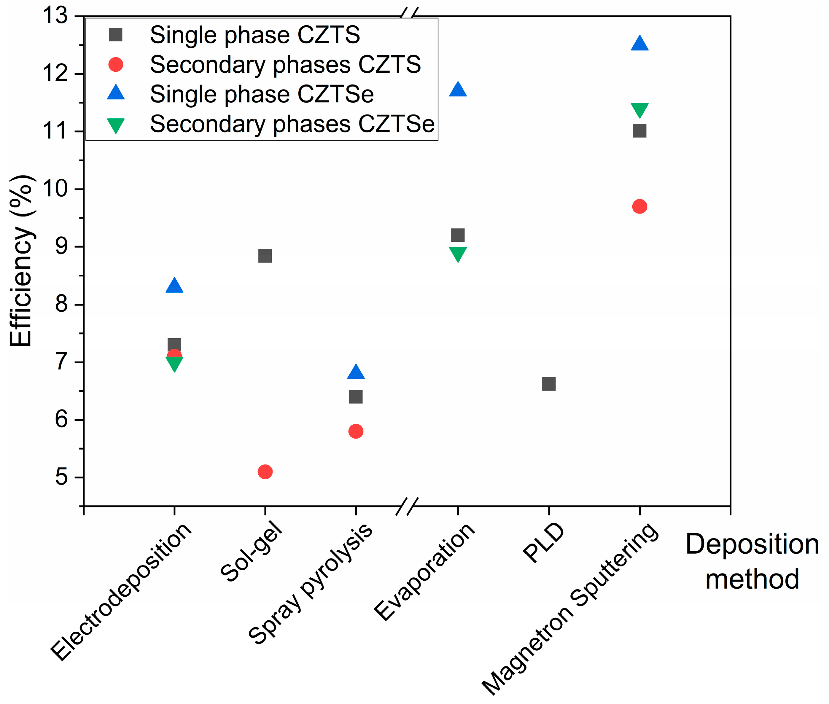
| Deposition Method | PCE (%) | |||
|---|---|---|---|---|
| Single Phase CZTS | Secondary Phases CZTS | Single Phase CZTSe | Secondary Phases CZTSe | |
| Electrodeposition | 7.30 [145] | 7.10 [118] | 8.20 [146] | 7 [114] |
| Sol-gel | 8.84 [147] | 5.10 [148] | - | - |
| Spray pyrolysis | 6.40 [149] | 5.80 [160] | 6.80 [150] | - |
| Evaporation | 9.20 [151] | - | 11.70 [152] | 8.90 [153] |
| PLD | 6.62 [154] | - | - | - |
| Magnetron sputtering | 11.01 [157] | 9.70 [158] | 12.50 [155] | 11.40 [156] |
Disclaimer/Publisher’s Note: The statements, opinions and data contained in all publications are solely those of the individual author(s) and contributor(s) and not of MDPI and/or the editor(s). MDPI and/or the editor(s) disclaim responsibility for any injury to people or property resulting from any ideas, methods, instructions or products referred to in the content. |
© 2024 by the authors. Licensee MDPI, Basel, Switzerland. This article is an open access article distributed under the terms and conditions of the Creative Commons Attribution (CC BY) license (https://creativecommons.org/licenses/by/4.0/).
Share and Cite
Zaki, M.Y.; Velea, A. Recent Progress and Challenges in Controlling Secondary Phases in Kesterite CZT(S/Se) Thin Films: A Critical Review. Energies 2024, 17, 1600. https://doi.org/10.3390/en17071600
Zaki MY, Velea A. Recent Progress and Challenges in Controlling Secondary Phases in Kesterite CZT(S/Se) Thin Films: A Critical Review. Energies. 2024; 17(7):1600. https://doi.org/10.3390/en17071600
Chicago/Turabian StyleZaki, Mohamed Yassine, and Alin Velea. 2024. "Recent Progress and Challenges in Controlling Secondary Phases in Kesterite CZT(S/Se) Thin Films: A Critical Review" Energies 17, no. 7: 1600. https://doi.org/10.3390/en17071600