Article

Design, Simulation, and Fabrication of a 500 kV Ultrawideband Coaxial Matched Load and Its Connectors for Fast Transient Pulse Measurement Systems

1
Laboratoire National de Métrologie et d’Essais (LNE), 29 Avenue Roger Hennequin, 78197 Trappes, France
2
Group of Electrical Engineering-Paris (GeePs), CNRS, CentraleSupélec, Université Paris-Saclay and Sorbonne Université, 11 rue Joliot-Curie, Plateau de Moulon, 91192 Gif-sur-Yvette, France
*
Author to whom correspondence should be addressed.
Energies 2024, 17(1), 166; https://doi.org/10.3390/en17010166
Submission received: 15 November 2023 / Revised: 19 December 2023 / Accepted: 22 December 2023 / Published: 28 December 2023
(This article belongs to the Topic High Voltage Systems and Smart Technologies)

Abstract

:
In the past few decades, Pulsed Power (PP) has been one of the fastest growing technologies, with more and more systems frequently emerging in domains such as civil, medical and military. These systems are based on high-voltage pulses, up to several hundreds of kilovolts, with temporal parameters ranging from microsecond levels to sub-nanosecond levels. One of the biggest challenges in this technology is the accurate and precise measurement of the generated PP. The PP measurement systems must possess high-voltage and wideband properties simultaneously, which is often conflicting. The central elements of a PP measurement system are a voltage divider and a termination load. The work presented in this article is dedicated to the second element of the PP measurement system. This paper describes the development of a 50 Ω coaxial termination load and its connectors for a high power ultrawideband (UWB) pulse measurement systems. The principle roles of these devices are to serve as a dummy matched load for the former and to facilitate the connections between different components of the pulse measurement system for the latter. These devices are designed to withstand pulse voltage amplitudes at least up to 500 kV with temporal parameters, such as rise time and pulse duration, varying from nanosecond to sub-nanosecond ranges. The main challenge in the development of a high-voltage UWB termination load is the tradeoff between the high-voltage and wideband characteristics, both of them requiring opposite dimensional aspects for the load device. This challenge is overcame by the special exponential geometry of the load device. The design employs a 30 cm long low-inductance tubular ceramic 50 Ω resistor, enclosed in a critically dimensioned shielding conductor of an exponential inner profile. This shrinking coaxial structure makes it possible to maintain a good level of matching all along the 50 Ω load. The results obtained through 3D electromagnetic modeling and vector network analyzer measurements show good agreement and confirm the reflection coefficient below −27 dB up to at least 2.5 GHz for the load device. Moreover, calculations demonstrate that the load device is very well adapted for nanosecond and sub-nanosecond pulses with voltage peaks as high as 500 kV. These results demonstrate the high-voltage and UWB properties of the developed load device and prove the utilization of this device in the measurement systems for the accurate and precise measurements of the PP.

1. Introduction

The domain of Pulsed Power (PP) refers to technologies where energy is accumulated during a relatively long period of time and then released in a short period, in the form of pulses, to deliver a very large amount of power to a given load or in other words to a given application. Since their establishment in the 1960s, these technologies have found applications in various domains and have now become one of the rapidly growing areas of research [1,2,3,4,5,6,7,8,9]. This is principally due to the fact that these pulses have relatively low energy content though they are capable of delivering very high levels of power. Historically, typical loads were primarily defense- and military-related applications, such as, among others, high-frequency transmitters, radars, satellites, space probes, pulsed power thrusters and intense electromagnetic interference antennas. However, after declassification of many of these works, several civil and medical applications have emerged in recent years. Among them, the most important ones are ground penetration radars (GPR) [10,11,12], X-ray machines [13,14], cancer treatment [15,16,17,18,19], monitoring of human organs [20], pasteurization of food [21] and electromagnetic vulnerability testing of electronic equipment [22], proving the strong potential for innovation that lies behind these technologies. For these applications, nanosecond and sub-nanosecond pulsed power needs to be measured with good levels of accuracy in order to achieve better control of the voltage impulses used in terms of amplitude and time parameters. This will provide a better knowledge of the pulse and avoid any side-effects and unnecessary irradiation of the targeted objects. The measurements of the pulsed power are often carried out through voltage sensors [23,24,25,26,27,28]; however, another important element in the measurement setup is the load device. It fulfills two important roles. The first one is the termination impedance matching to the characteristic impedance of the transmission line coming from the pulse source. The second one consists of the dissipation of the energy present in the incident high-voltage pulse. Consequently, for the high-voltage UWB pulse termination load, a fast response time, low-inductance with a wide frequency bandwidth ( f c ), at least up to 2.5 GHz for sub-nanosecond pulses of rise times ( t r ) down to 140 picosecond, f c = 0.35 t r [29], and high insulation properties must be achieved simultaneously. Several measurements systems based on a voltage divider and a matched load have been published [2,24,28,30,31,32,33,34,35,36,37,38,39,40,41,42]. However, three main issues can be identified in the termination load devices used in these setups:
  • They do not have a sufficient broadband frequency to measure pulses with rise times in the range of few hundreds of picoseconds and fall times going down to a few tens to hundreds of nanoseconds.
  • More importantly, the amplitudes levels are limited only up to a maximum of a few hundred kilovolts. Therefore, these systems are not suited to measure voltage amplitudes up to 500 kV levels.
  • The absence of connectors makes these systems rigid and they lack flexibility which makes it difficult to calibrate each component separately to avoid their footprint.
In this work, a UWB 50 Ω load device capable of withstanding voltage peaks up to 500 kV is obtained with a special load geometry, which is studied thoroughly and presented together with the electromagnetic modeling and the mechanical conception. In addition, the connectors capable of withstanding voltage peaks as high as 500 kV are unavailable in the market. Connectors are therefore developed with a 50 Ω characteristic impedance, as the main transmission line characteristic impedance, and are capable of providing good insulation to the voltage amplitudes at least up to 500 kV for nanosecond and sub-nanosecond pulses.
The article is arranged as follows. Section 2 describes the conception of a UWB 500 kV coaxial 50 Ω device, including the choice of the different elements such as the 50 Ω resistor and the main line insulator. The theory behind a reflection-free load device together with the electromagnetic simulations with real materials fed into the model as a proof of concept are also presented in this section. In Section 3, details about the fabrication of the high-voltage connectors and their transition cones (transmission lines with progressively varying diameters) are presented. Section 4 is devoted to the high-frequency and high-voltage characterization of the devices developed in this work, and the obtained results are presented and discussed. Section 5 briefly gives an overall view of this work describing the main challenge, methodology and assumptions. Finally, Section 6 summarizes the main achievements of this paper.

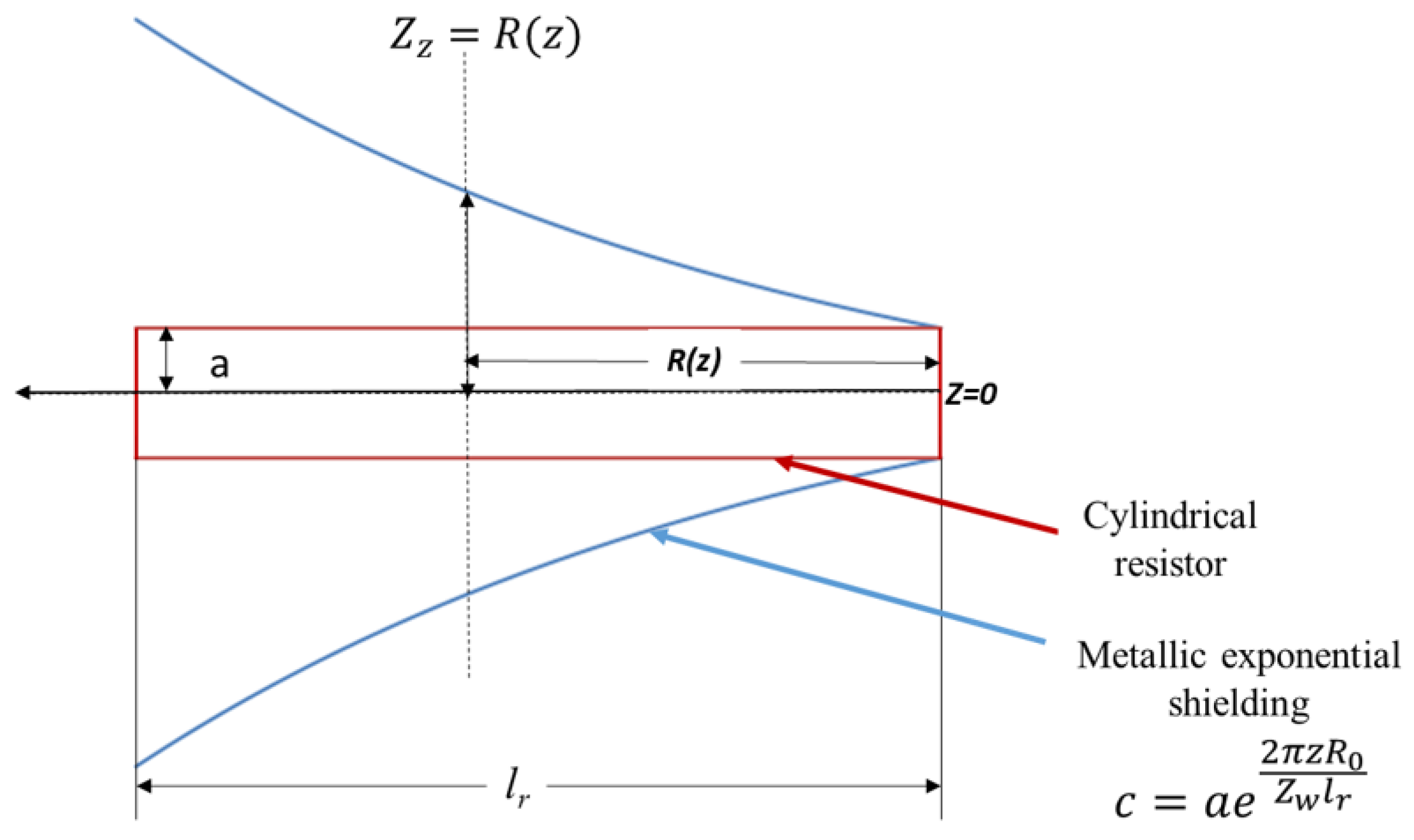
2. Conception of Broadband 500 kV Coaxial 50 Ω Load

A coaxial termination load mainly consists of three elements, namely, a resistor as the central line element, a metallic shielding and an insulator between them, as presented in Figure 1. In the domains where high power as well as high frequency is concerned, such is the case in this work, the transmission line terminations should be built in such a way that the incoming energy from the incident pulse is absorbed as much as possible, which would result in a minimum reflection of the incident pulse. The following sub-sections describe the optimization of the main elements necessary to fabricate a broadband 50 Ω load device capable of withstanding voltage peaks as high as 500 kV.

2.1. Choice of the 50 Ω Resistor

For high power, an important property of the load device is to guarantee a sufficient high-voltage insulation. However, the inevitable presence of the thin layers or pockets of air at the resistor–insulator interface and even in the tubular cavity of the resistor could drastically reduce the dielectric strength of the whole load device and could eventually cause flashovers between the metallic contacts of the resistor. As a solution, relatively long resistors are used as the resistive element constituting the PP coaxial loads. Therefore, for the conception of the 50 Ω termination load device, the choice of an appropriate resistor for the coaxial load is critical. It should possess the following properties:
  • A low-inductance resistor with a DC resistance value of 50 Ω.
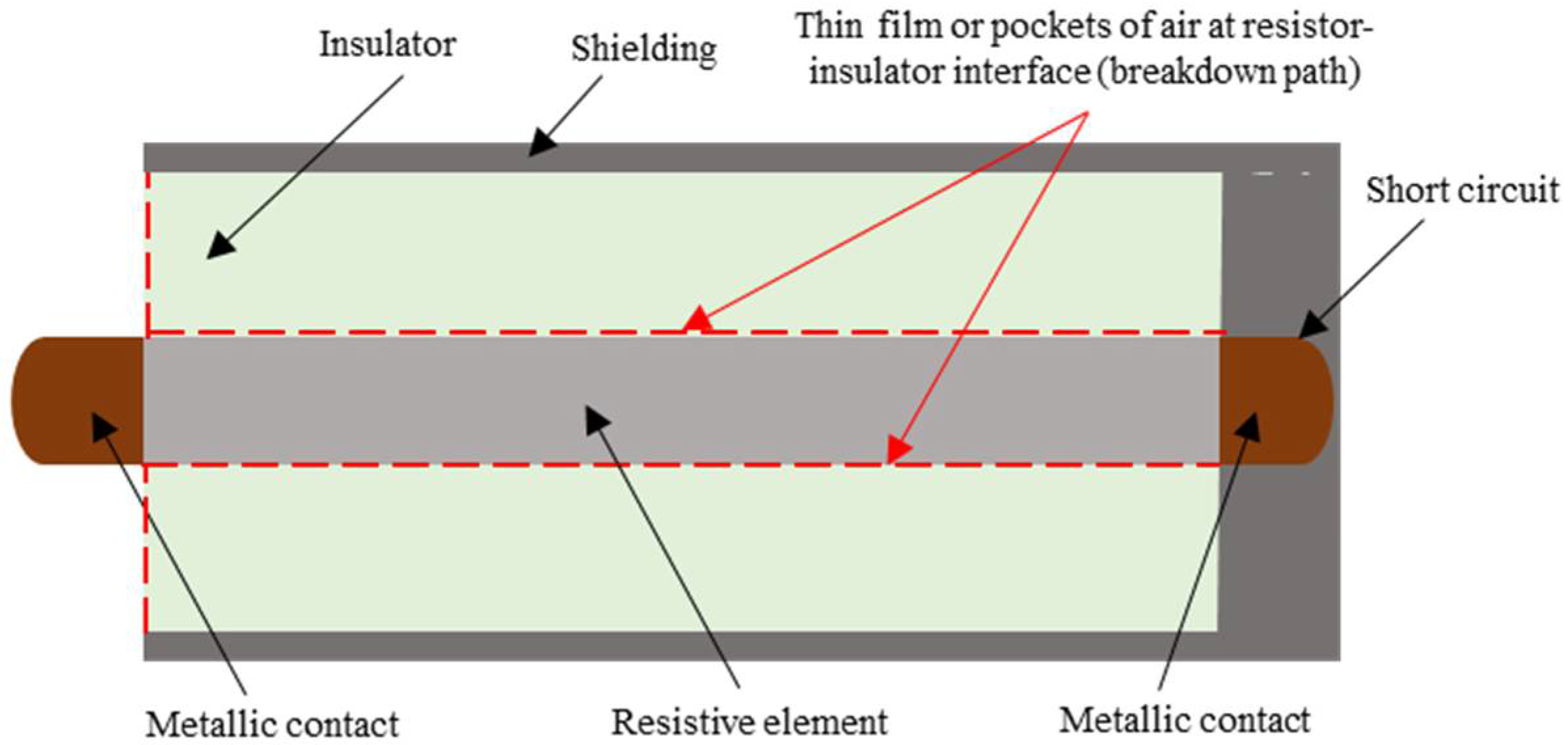
  • A sufficient high-voltage insulation and an adequate level of separation between the metallic contacts of the resistor to avoid flashovers. These flashovers could also appear at the resistor–insulator interface, as indicated in Figure 1 by the dotted line representing air pockets. The flashovers could be transmitted to the measuring instruments present in the measurement circuit, resulting in their breakdown.
  • A bulk resistor for better energy dissipation. The load, apart from its principal role of matched termination of the transmission line, is also destined for the dissipation of the energy present in the incident pulse. Bulk resistors facilitates this process.
  • High specific heat of the resistive material used to avoid excess heating of the load. Materials with low specific heat constituting the resistor could rise rapidly in temperature and cause extra heating of the load. This heating could therefore change the value of the resistor and the 50 Ω value of the load resistor will not be assured.
In search of the abovementioned properties, different resistors, such as wire-wound resistors and thin film resistors, were tested. However, for the lengths of resistors necessary to avoid flashovers between their metallic contacts for voltage peaks up to 500 kV, these long resistors presented high inductance values and poor energy dissipation properties. Finally, a tubular low-inductance bulk ceramic resistor with embedded metallic conducting particles was chosen. Unlike a film resistor, which typically comprises a “thin” or “thick” conductive film deposited or printed onto a non-conductive, insulating flat or tubular, usually ceramic, substrate, the chosen ceramic composition resistors consist of a matrix of conductive metallic particles that are mixed with ceramic materials, formed into a desired shape and then fired at very high temperatures. Furthermore, the bulk construction advantageously produces an inherently low-inductance resistor, a property inversely proportional to the bandwidth of the resistor. This construction facilitates a uniform distribution of energy and power throughout the entire ceramic body, which helps to withstand high operating temperatures with, at the same time, high power dissipations.
A 30 cm long 50 Ω (50 Ω ± 10%) nominal value resistor (889SP500) based on this manufacturing process from OHMITE was chosen. The separation between the metallic terminations (length of the resistive bulk) is 26 cm, which is more than sufficient to avoid flashovers between them due to the presence of air. Indeed, to avoid flashovers in the air, which has generally a dielectric breakdown strength of around 30 kV/cm, a minimum distance of at least 17 cm is needed for pulses of peak voltages of 500 kV.

2.2. Main Line Insulator

Virgin-grade PTFE was chosen to be the dielectric present between the 50 Ω resistor and the shielding for its low dielectric constant and high dielectric strength. The PTFE dielectric was characterized in terms of its complex relative permittivity ( ε 1 ) and loss tangent (tan δ) up to 1 GHz through S-parameter measurements using a vector network analyzer (VNA) and the method described by Nicolson and Ross [43]. For these measurements, a cylindrical sample of length d = 5 cm of the PTFE is placed in a coaxial waveguide of characteristic impedance Z0 with only air as a dielectric, without the sample. The measurement is performed after calibrating the VNA using a “Through, Reflect, Line” method, and the S-parameters of the coaxial guide were measured [44,45]. This waveguide is presented in Figure 2, where ε 1 and μ 1 represent the complex relative permittivity and relative permeability of the PTFE sample, respectively, and Z represents the new characteristic impedance of the same coaxial waveguide with the PTFE sample as dielectric material.
Through the measured S-parameters (S11 and S21), the relative complex permittivity of the PTFE is obtained by Equation (1) [43]:
ε 1 = j 1 R 1 + R c 0 ω d × l n T
where c 0 is the speed of electromagnetic wave in vacuum, ω is the angular frequency and the coefficients R and T are defined as follows:
R = S 11 2 S 21 2 + 1 2 S 11 ± S 11 2 S 21 2 + 1 4 S 11 2 + 1
and
T = 1 S 21 + S 11 R S 21 + S 11 R
The measured values of the real part of ε 1 and of tan δ through the VNA up to 1 GHz for the PTFE sample is presented in Figure 3. Their average values were found to be 2.03 ± 0.07 and 0.003 ± 0.006, respectively, in the concerned bandwidth from 50 MHz to 1 GHz for 340 equally spaced measurement points. The measurement uncertainties are given with a coverage factor of k = 2. The measurement values of the real part of ε 1 and tan δ are fed into the EM simulations of the designed load, presented in Section 2.4, within the measurement uncertainty limits.

2.3. Theoretical Analysis of a Reflection-Free Load

The characteristic impedance Z 0 of a loss-free coaxial transmission line can be determined by Equation (4):
Z 0 = 1 2 π μ 0 μ 1 ε 0 ε 1 ln c a
where:
  • μ 0 : permeability of free space ( μ 0 = 1.25663706212 × 10⁻⁶ H/m);
  • μ 1 : relative permeability of the dielectric of the transmission line;
  • ε 0 : permittivity of free space ( ε 0 = 8.8541878128 × 10⁻¹² F/m);
  • ε 1 : relative permittivity of the dielectric of the transmission line;
  • c: inner radius of the metallic shielding of the transmission line (m);
  • a: radius of the central conductor of the transmission line (m).
Furthermore, the reflections are quantified by the scattering reflection coefficient (S11), shown in Equation (5) for a uniform coaxial transmission line with characteristic impedance Z 0 , terminated by a load of impedance Z L :
S 11 = Z L Z 0 Z L + Z 0
It can be easily concluded from (5) that for the case where the transmission line is terminated by an impedance equal to its characteristic impedance, i.e., ZL = Z0, the refection coefficient value will be zero and the incident pulse can be measured accurately. However, it is difficult to develop a broadband termination load with a zero-reflection coefficient value, especially in the high-voltage domain that imposes uncompressible dimensions of the elements used to fabricate the load device for a sufficient level of high-voltage insulation. The values of S11 directly contribute to the measurement uncertainty and, consequently, larger values of |S11| could lead to increased measurement uncertainty. For example, in the case of modeling of a normal cylindrical 50 Ω termination load through CST Microwave Studio®, presented in Figure 4a, with a 30 cm long and 12.7 mm radius ceramic resistor enclosed in an aluminum shielding with a radius of 42.55 mm with PTFE as insulator between them, it can be observed that a significant amount of the incident signal is reflected back, as high as 20%, due to mismatching, as shown in Figure 4b.
This level of reflection as obtained is principally due to the size of the resistor. At higher frequencies, in the case of rapid pulses, this resistor lose its discrete properties since its length is no longer negligible in comparison to the wavelength of the travelling pulses. This phenomenon results in a mismatching of the load impedance to the characteristic impedance of the transmission line, causing a significant amount of reflection. It could cause, then, a superposition of the reflected pulse to the measured pulse and, in some cases, it becomes difficult to discriminate from the real pulse and the reflected one.
Nevertheless, the reflection coefficient value can be minimized through some special geometrical compensations. Theoretically, to obtain reflection-free performance of the load, as demonstrated by Harris [46], the characteristic impedance of the coaxial line enclosing the resistor at any cross section must be equal to the load resistance beyond that cross section. Considering R0 as the total resistance of the resistor and R(z) being the remaining ohmic resistance at a distance z from the short-circuited end of the resistor of total length lr, then R(z) can be written as follows [47]:
R z = z R 0 l r
Therefore, for reflection-free transmission, as stated before, the value of R(z) must be equal to the local characteristic impedance Z0(z) of the coaxial line at any point z, which is given by Equation (4). This leads from the Equations (4) and (6) to the following equality:
z R 0 l r = 1 2 π μ 0 μ 1 ε 0 ε 1 ln c a
From Equation (7), given that a is a constant determined by the radius of the resistor, the required profile of the outer radius c of the metallic shielding can be calculated as follows:
c = a e 2 π z R 0 Z w l r
where Z w = μ 0 μ 1 ε 0 ε 1 is the plane wave characteristic impedance in the dielectric of the coaxial line.
Equation (8) results in an exponential profile for the shielding, shown in the Figure 5.
There are further improvements in the shielding conductor profile which have been published in the literature [47,48], such as tractorial terminations based on a tractrix profile, which is a steeper form of the exponential profile. However, for the resistive loads with a long resistive element for better insulation from flashovers, the difference in the results announced are not that overwhelming [47].

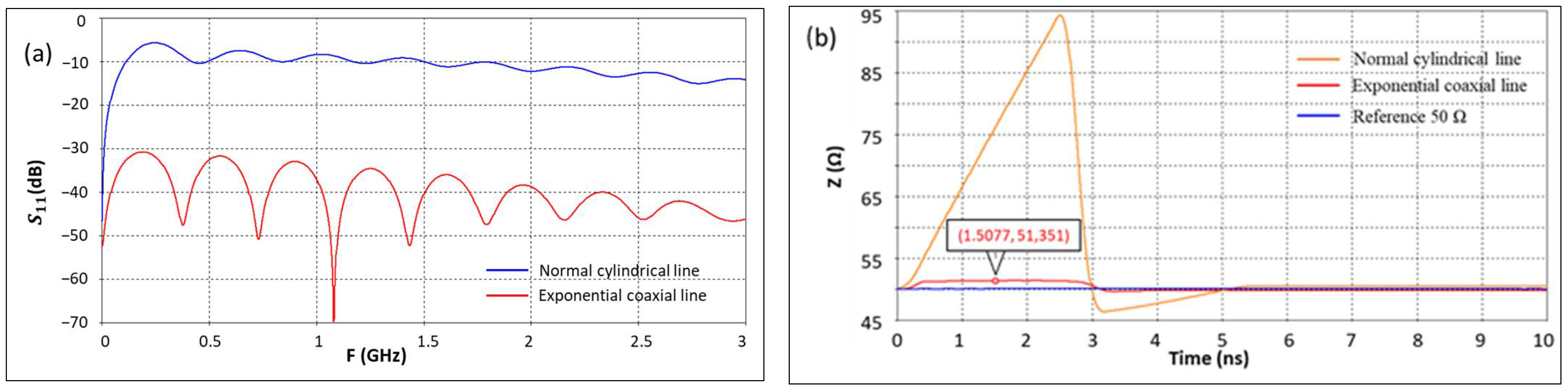
2.4. Electromagnetic Simulation of Exponential 50 Ω Load

The CST Microwave Studio® software is used to perform the electromagnetic modeling and the optimization of the 50 Ω load device based on the exponential profile of the shielding conductor given by Equation (8). To evaluate their differences, both a normal cylindrical profile as in Figure 4 and an exponential coaxial profile as in Figure 5 for the same resistor and the same insulating material are modeled. A 50 Ω tubular ceramic resistor 30 cm in length was modeled as the central conductor with an outer radius (a) of 12.7 mm. This resistor was put in a normal cylindrical coaxial line with an inner radius of the shielding aluminum conductor (c) of 42.55 mm, calculated to attain a 50 Ω characteristic impedance all along the resistor length with PTFE as the dielectric. Later, the exponential profile was modeled for the shielding conductor. The results of this modeling in terms of reflection coefficient and Time-Domain Reflectometry (TDR) response are presented in Figure 6a and Figure 6b, respectively.
The modeling results presented in Figure 6 prove the better matching capabilities of the 50 Ω load based on exponential geometry, which is a key requirement for the accurate and precise measurements of the pulses through the pulse measurement systems. In light of the superior quality of the frequency adaptation results obtained from the modeling of the exponential geometry, a coaxial 50 Ω load device is fabricated and characterized. The characterization results will be presented in the Section 4, after the development of the load connection devices shown in Section 3.

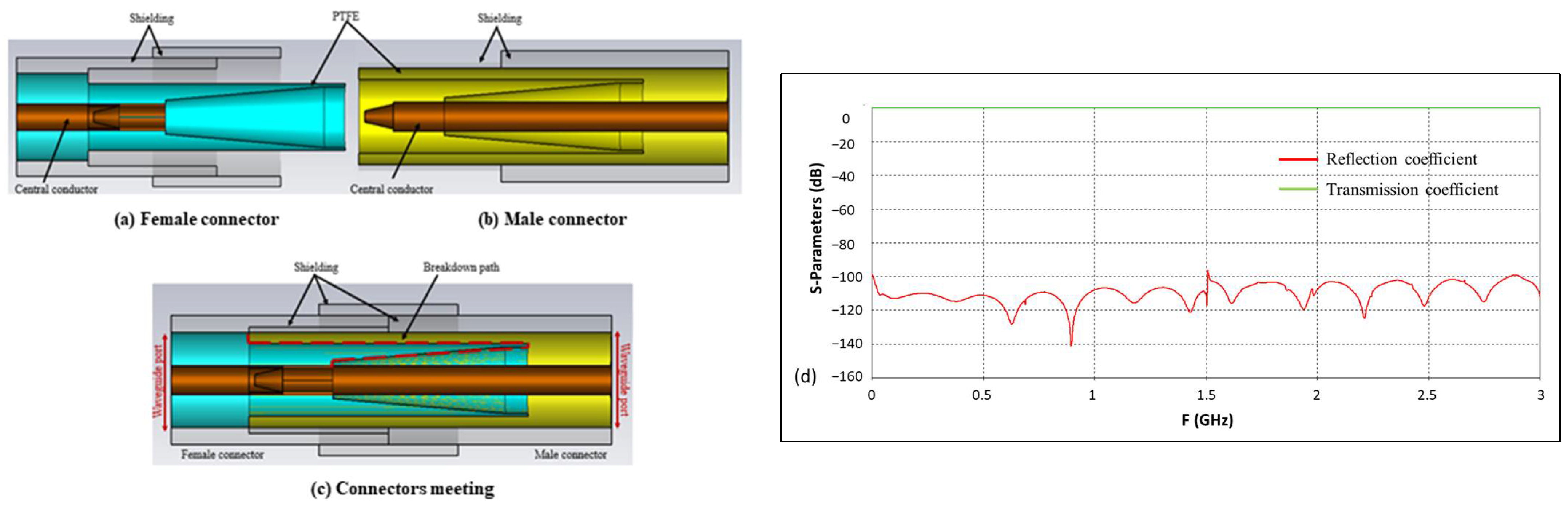
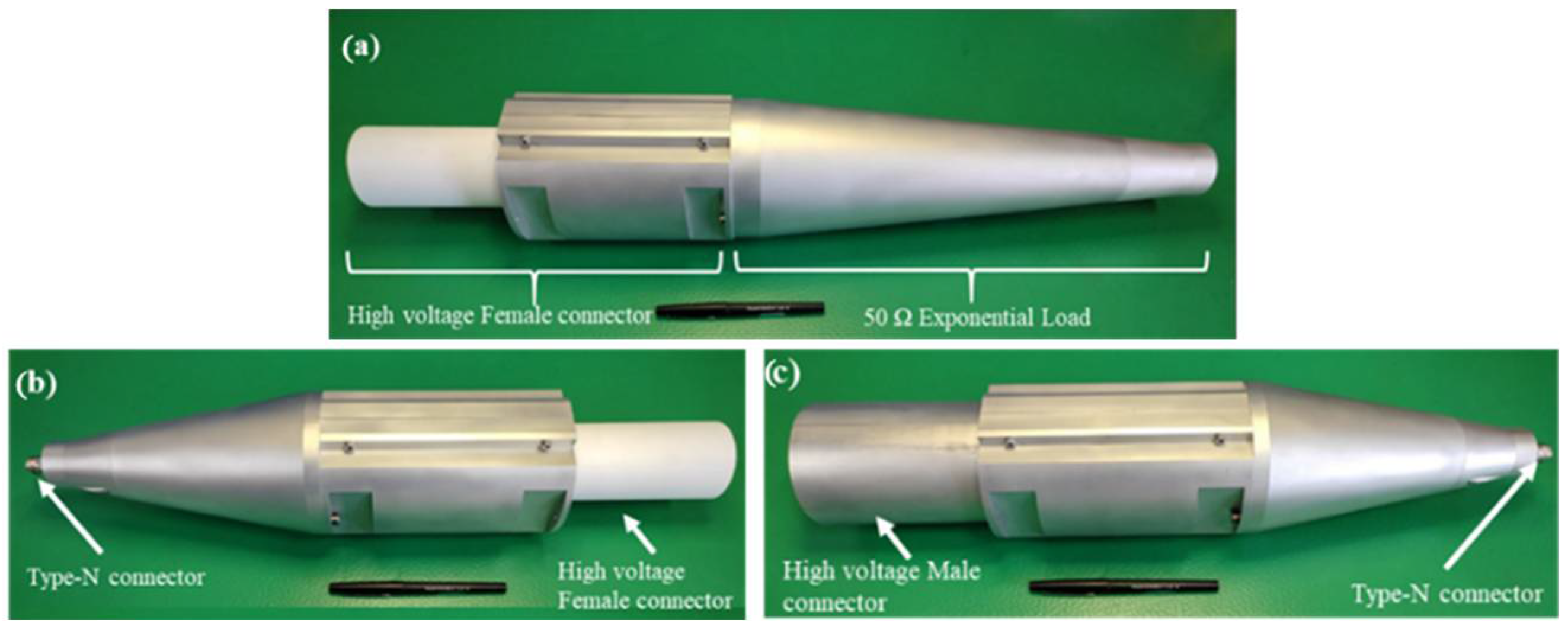
3. Development of High-Voltage Connectors and Transition Cones
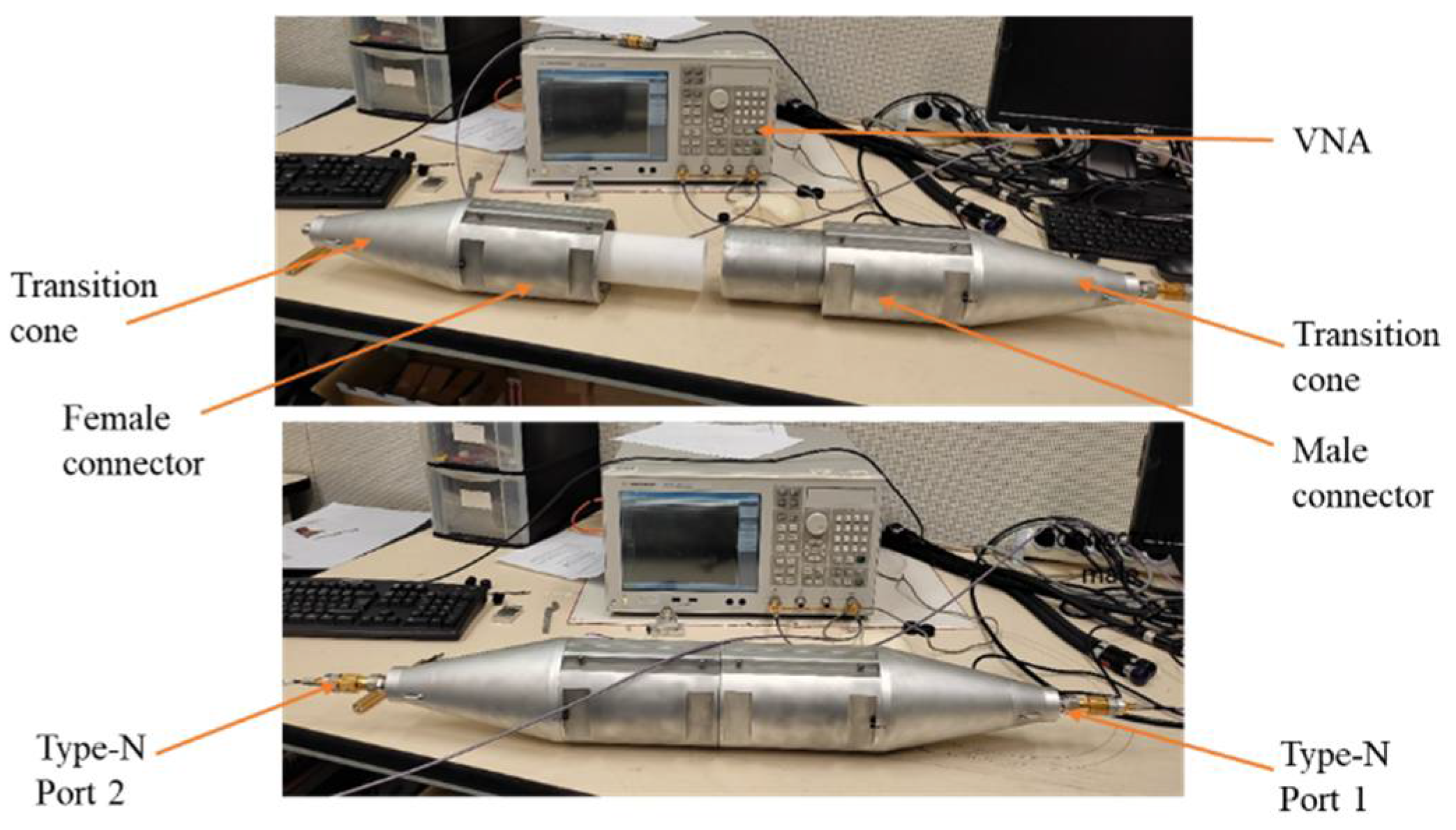
The connectors are necessary to connect the different elements of a measurement system together, such as the load to the voltage probes and even the complete measurement system to the PP generator for measurements. In the best-case scenario, to avoid any further adaptations and mismatching problems, their dimensions and the characteristic impedance should be equivalent to that of the elements they would connect together. However, connectors capable of withstanding voltage peaks of 500 kV are unavailable in the market. The geometry of the female and male connectors developed in this work are presented in Figure 7a and Figure 7b, respectively. They possesses a 50 Ω characteristic impedance and are capable of providing good insulation to the voltage amplitudes at least up to 500 kV for nanosecond and sub-nanosecond pulses.
Sufficient security measures against flashovers and dielectric breakdown are taken in the design of these connectors. This is principally due to the meeting surfaces of the dielectric in the connector which could cause flashovers if they are not designed properly with respect to the dielectric breakdown strength of the air. The Breakdown path is mentioned in Figure 7c. Hence, the breakdown path for the connectors is designed to be 27 cm with 10 cm of margin from the actual length needed.
The mating geometry of the connectors, presented in Figure 7c, is modeled on the CST software using real material properties, such as aluminum for the shielding, PTFE as the dielectric and copper as the central conductor. The waveguide ports are placed at the extremities and the results obtained in terms of the reflection coefficient (S11) and the transmission coefficient (S21), presented in Figure 7d, are analyzed. Extremely low values of around −100 dB are obtained for the reflection coefficient, whereas the transmission coefficient values were found to be around 0 dB for frequencies up to 10 GHz, proving that the integration of these connectors in the measurement system to connect different components together would have negligible effects on the measured waveform. Furthermore, these connectors can be easily adapted to be inserted in any coaxial device through adaptors that can be easily designed.
To facilitate the VNA characterization of the exponential 50 Ω load, transition cones with progressively varying diameters are developed to keep a constant characteristic impedance while ensuring a transition between the dimensions of the high-voltage connectors and the Type-N connectors, which are present at the input of the VNA. These VNA characterizations are performed in terms of S-parameters at low power levels. The transition cones possess male or female high-voltage connectors at one end, and Type-N connectors at the other end. Photographs of the fabricated 50 Ω load device and transition cones are presented in Figure 8.

4. Characterization

During the first phases of validation and testing, each of the developed components, such as the 50 Ω exponential load, high-voltage male and female connectors and the transitions cones, are tested mechanically for their final dimensions and integration into each other. After these mounting tests, each of them are characterized separately, thanks to the connectors developed, in order to measure their frequency responses from tens of kilohertz to a few gigahertz in terms of S-parameters through a VNA. These results are then compared to results obtained from the EM modeling of the same components using CST Microwave studio®. On the other hand, the high-voltage characteristics of the 50 Ω exponential load are confirmed through the heat dissipation properties of the 50 Ω bulk ceramic resistor and through the calculation of the temperature rise in such by the passage of a modeled 500 kV pulse.
An Agilent VNA E5071C [49] with a frequency bandwidth ranging from 9 kHz to 4.5 GHz is used for the S-parameter measurements. Prior to the measurements, the VNA is calibrated to remove the systematic errors terms: directivity, source match, reflection tracking, transmission tracking and load match. This calibration is performed through the “unknown thru method” [50]. This method is based on the use of three impedance standards (open, short and 50 Ω loads) and an additional unknown thru connection. This latter is a transmission line for which the characteristics are determined during the calibration process.

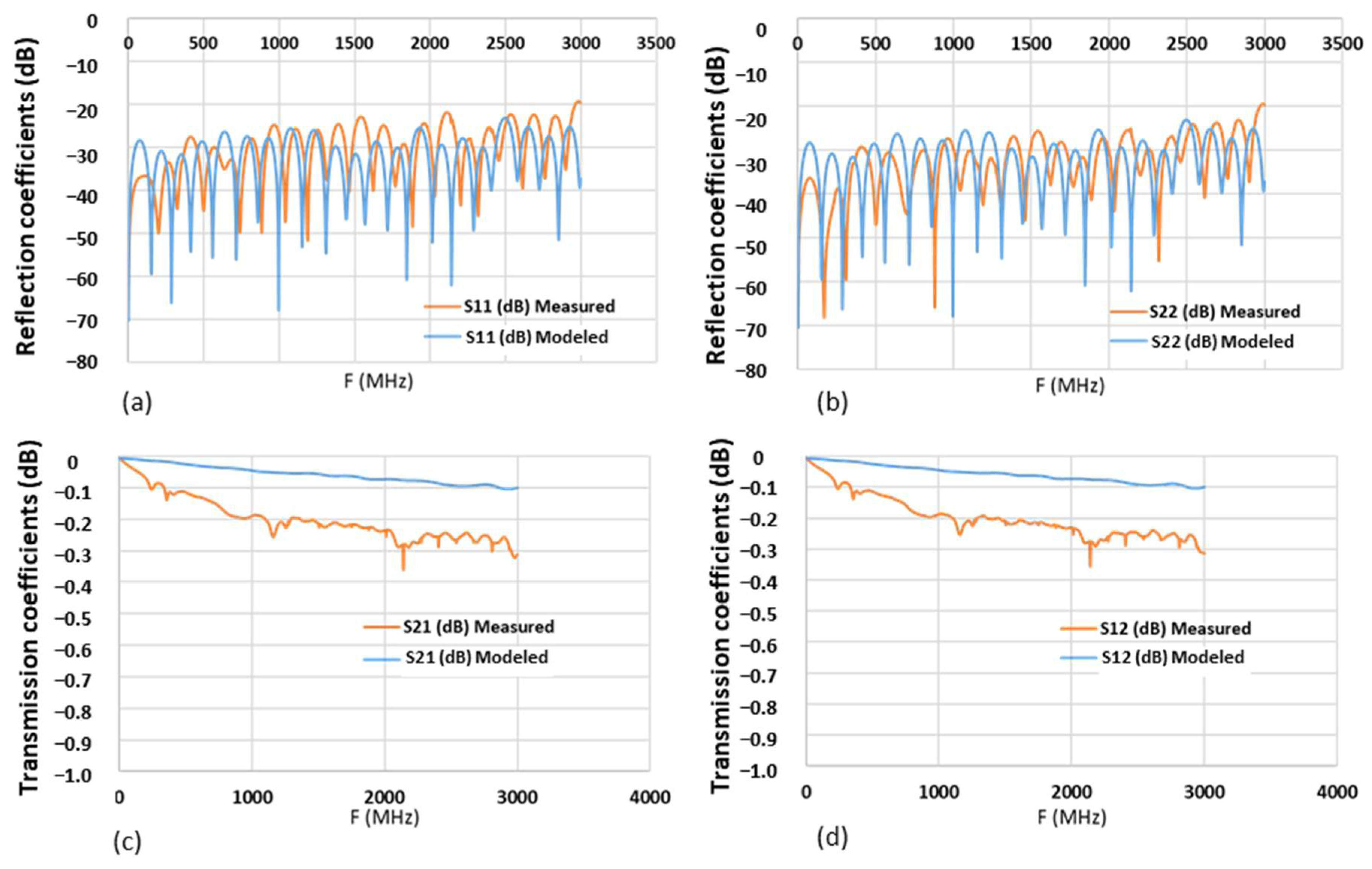
4.1. Characterization of Connectors and Transition Cones

The frequency responses in terms of S-parameters of the high-voltage connectors with the transitions cones are measured through the calibrated VNA to evaluate their footprints. The two-port measurement setup is presented in Figure 9, where the two Type-N output connectors of the transition cones are connected to the VNA inputs. A comparison between the moduli of the S-parameters obtained through these measurements and the CST modeling up to 3 GHz is presented in the Figure 10.
It can be observed from Figure 10 that the reflection coefficients (S11 and S22) are in very good agreement between the modeled and the fabricated transition cones with high-voltage connectors. However, a small difference can be noticed in the comparisons between the measured and modeled transmission coefficients (S12 and S21). This is principally due to the mechanical imperfections in the realization of the conical cavity, for the central conductor, of the PTFE dielectric used in the transitions. Indeed, during the fabrication process, it was noticed that the 170 mm long conical cavity at the center of the PTFE cone presented some anomalies due to the passage of the drilling instrument and was not smooth. Taking into account the acceptable values of the measured transmission coefficient up to 2 GHz (−0.23 dB), it was decided to move forward with these imperfections.

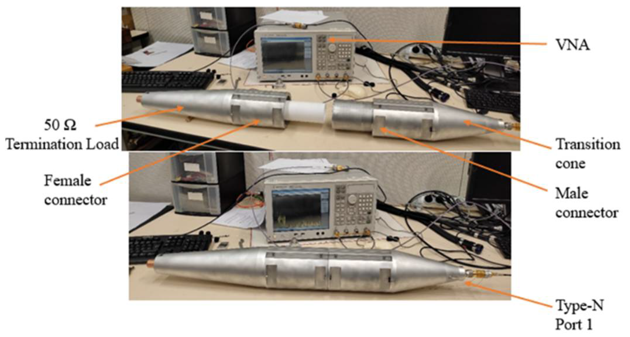
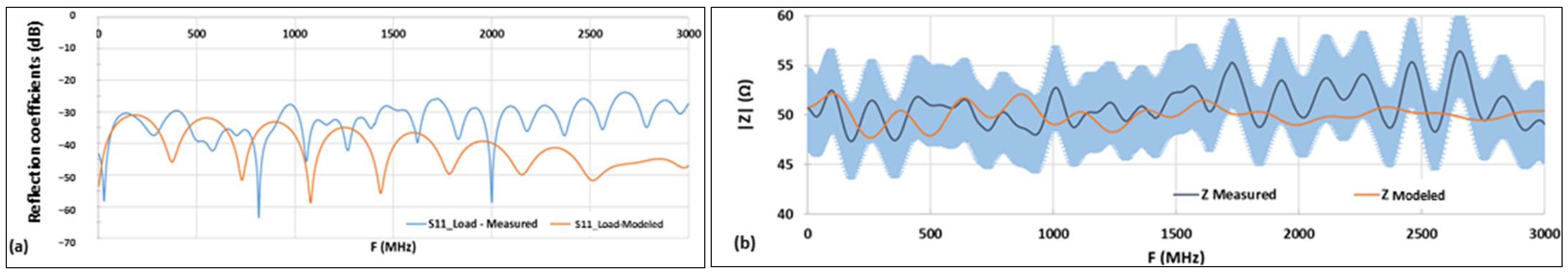
4.2. Characterization of 50 Ω Exponential Termination Load

The reflection coefficient of the fabricated 50 Ω exponential load is measured though the calibrated VNA. The one-port measurement setup is presented in Figure 11 and the comparison of measured and modeled results of the reflections coefficients and the modulus of the impedance (Z) at the input of the load are presented in Figure 12.
The results presented in the Figure 12 show that the measurements of the reflection coefficient of the 50 Ω exponential load are close to the modeling results, at least up to the concerned high-frequency limit of 2.5 GHz within the absolute measurement uncertainty of 5 Ω, obtained through statistical methods, with a coverage factor of 2. The maximum measured value of the reflection coefficient (S11) is found to be −27 dB up to 2.5 GHz. The small differences observed between the modeling and measurements are principally due to the mechanical tolerances that are necessary for the fittings of the different elements of the load and the high-voltage connector. Furthermore, these elements are of tens of centimeters in length, around 50 cm for the PTFE dielectric, for which the control and the corrections of the coaxiality are often difficult to perform.

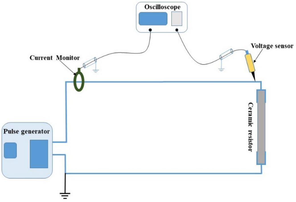
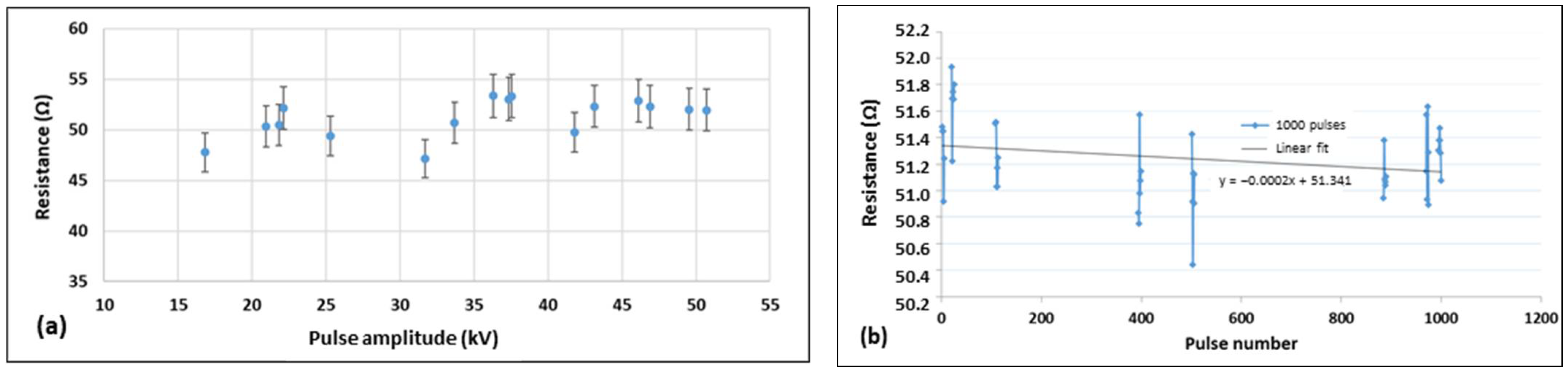
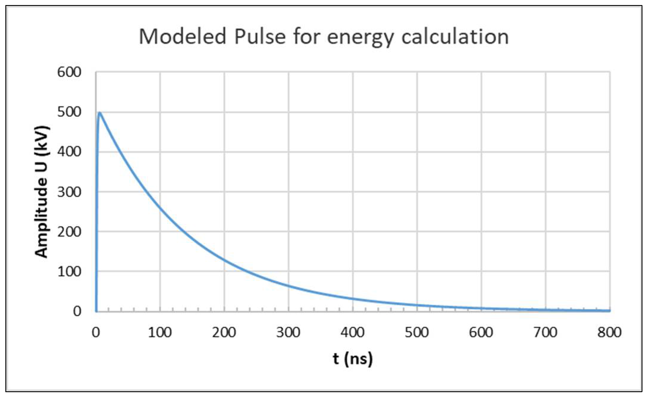
4.3. High-Voltage Characterization

A similar ceramic bulk resistor (889SP500) as mentioned in Section 2.1 with 51.5 Ω DC resistance is tested with applications of different pulses to evaluate the deviation of its resistance value from the DC value independently of the high-frequency characteristics of the resistor. The schematic of the measurement setup is presented in Figure 13.
The current pulse converted to a voltage pulse by the current sensor and the voltage pulse at the extremities of the resistor are measured simultaneously on an oscilloscope. The output of the current sensor is further converted to obtain the peak current value I p e a k and, through the voltage peak value measured by the voltage sensor V p e a k , the value of the resistance ( V p e a k / I p e a k ) is calculated. Pulses of voltage amplitudes varying from 17 kV to 50 kV with a rise time of 230 ns and a duration of 25 µs are generated from a high-power pulse generator and were applied to the ceramic resistor. These pulses, at a 50 kV voltage level, represent around three times the total pulse energy of a 500 kV pulse with a rise time of 1 ns and a duration of 100 ns. The resistance value is presented in Figure 14a as a function of the pulse amplitude. It can be noticed that the measured values of the resistance are in agreement with the DC value within the evaluated absolute measurement uncertainty of 2 Ω with a coverage factor of 2. In addition, to evaluate the heating effect of the resistor, 1000 continuous pulses at an interval of 1 s with pulses of 12 kV voltage amplitude and a rise time of 1.2 µs with a duration of 50 µs were applied to the ceramic resistor and the resistance values were calculated in the same way. These results are presented in Figure 14b, and demonstrate that the measured values are still in good agreement with the DC value of the resistance within the same measurement uncertainty value as above.
Furthermore, the temperature rise of the same resistor during the application of a 500 kV pulse is also calculated to evaluate the deviation of the resistance value with respect to the temperature coefficient of the resistor. The temperature coefficient announced by the constructor is between +0.2%/°C and −0.08%/°C. The local rise in temperature T of the resistor is calculated with the help of Equation (9).
T = E m C P
where:
  • E: total energy dissipated in the resistor;
  • m: mass of the resistor;
  • C P : specific heat of the resistor.
From the dimensions and the mass density of the resistor, the mass m was calculated to be 163.3 g and the specific heat indicated by the constructor was 0.25 cal/(g.°C), which can be written as 1.046 J/(g.°C). The energy accumulated in the resistor at a given time t is calculated by the following equation:
E = 0 t U t 2 R   d t
where R is the load resistance value of 50 Ω and U ( t ) represents the waveform of the input pulse. As an example, a double exponential pulse is considered which is defined by the following:
U t = A U e α t e β t
Using Equation (10), a 500 kV pulse is modeled with a rise time of around 5 ns and full-width at half maximum (FWHM) value of almost 100 ns that is also called the pulse duration. These pulse characteristics are the upper limits of the incident pulse in terms of peak voltages and temporal parameters, which are intended to be measured in this work. The parameters used to model this pulse are A = 1.0372, U = 500 kV, α = 7   µ s 1 and β = 1000   µ s 1 . The pulse waveform obtained through (11) is presented in Figure 15.
From Equations (10) and (11), the total pulse energy at a given time t is calculated by the following equation:
E = A 2 U × 10 3 2 R   1 2 α e 2 α t 1 + 1 2 β e 2 β t 1 + 2 α + β e α + β t 1  
Using (12), the value of the total energy E for the pulse presented in Figure 15 for FWHM of t = 100 ns is around 330 J, which represents a 2 °C rise in the resistor temperature calculated through Equation (9). This rise in temperature, for a 50 Ω resistor, represents a variation from 0.2 Ω to 0.08 Ω using the temperature coefficient values announced by the constructor. These relatively small variations in the value of the considered resistor are considered negligible.

5. Discussion

The main challenge in the development of a high-voltage UWB coaxial load device is the tradeoff between two domains that are exactly opposite to each other, namely, high voltage and high frequency. Indeed, the high-voltage domain dictates the principle of incompressible separations between conducting elements having a potential difference, whereas the high-frequency domain require extremely small dimensions compared to the wavelength for the conducting elements to avoid propagation effects. These requirements become more predominant as voltage amplitude and frequency are increased. The work presented in this article demonstrates a successful practical solution to the abovementioned issue. The exponential geometry and the components used to develop the 50 Ω load allow this device to be compatible with both domains. The results presented in Section 4.2 and Section 4.3 prove that the UWB and high-voltage-withstanding properties are simultaneously obtained for the load device.
A critical designing process was used in the development of the exponential 50 Ω load device. The theoretical approach behind the exponential geometry of the load device is validated through electromagnetic modeling with real material properties fed into the model. The load device is then fabricated following the dimensions used in the modeling. The results obtained from the VNA characterization and the electromagnetic modeling are compared, and good agreement is obtained between both results. The theoretical analysis of the load device and the measurements carried out on the 50 Ω resistor in Section 4.3 prove that the developed exponential load device is very capable of withstanding voltage peaks as high as 500 kV for nanosecond and sub-nanosecond pulses. Based on the theoretical analysis, the authors are confident that the UWB 50 Ω load device presented in this paper is capable of withstanding voltage peaks even higher than the 500 kV levels for nanosecond and sub-nanosecond pulses.

6. Conclusions and Outlook

In this article, a new UWB high-voltage 50 Ω dummy load for nanosecond and sub-nanosecond pulse measurement systems up to 500 kV is presented. High-voltage and high-bandwidth characteristics have been demonstrated simultaneously for this dummy load. Such properties are almost nonexistent for a single device in the literature. The S-parameter measurements through a calibrated VNA are compared to the EM simulations in the concerned frequency domain and are found to be in good agreement. The main features of the matched load are the capability of withstanding pulse voltage peaks up to at least 500 kV and a maximum reflection coefficient (S11) of −27 dB for frequencies up to 2.5 GHz, which guarantees a negligible amount of interference for the measured pulses at the output of the measurement systems for high levels of accuracy. Other components that are unavailable in the market for these voltage levels, such as high-voltage male and female connectors and transitions cones, are also developed. The factors affecting the frequency responses of these components and, even more importantly, their voltage-withstanding capabilities for voltage peaks up to 500 kV are discussed. Another important aspect of this work is that the dummy load can be easily mounted to any pulse measurement system of 50 Ω characteristic impedance through these connectors with the help of adaptors that can be easily designed for this purpose. Furthermore, following the same design, other dummy loads with different impedance values can be developed as required.
This work paves the first step toward the accurate and precise measurements of high-voltage pulses in the nanosecond and sub-nanosecond domain, constituting the key element of the PP systems. Indeed, the characterization of these high-voltage fast pulses with low levels of uncertainty will help National Metrology Institutes (NMIs) to respond to the need for the metrological traceability to the International Systems of units (SI) of PP in the nanosecond and sub-nanosecond range, which is almost absent today.

Author Contributions

Conceptualization, M.S.K., M.A. and Y.L.B.; methodology, M.S.K., M.A. and Y.L.B.; validation, M.S.K., M.A. and Y.L.B.; formal analysis, M.S.K., M.A. and Y.L.B.; investigation, M.S.K., M.A. and Y.L.B.; data curation, M.S.K.; writing—original draft preparation, M.S.K.; writing—review and editing, M.A. and Y.L.B. All authors have read and agreed to the published version of the manuscript.

Funding

This research received no external funding.

Data Availability Statement

The data supporting the presented results are publicly available online in the achieved Ph.D. thesis at https://theses.hal.science/tel-04032644, published on 16 March 2023.

Acknowledgments

The authors would like to thank Tony Delauney, Michael Coince, Camus Morris, Fabrice Becuwe and Thierry Cernic (LNE) for their valuable advices in the mechanical conception of the devices developed in this work.

Conflicts of Interest

The authors declare no conflicts of interest.

References

  1. Prather, W.D.; Baum, C.E.; Torres, R.J.; Sabath, F.; Nitsch, D. Survey of Worldwide High-Power Wideband Capabilities. IEEE Trans. Electromagn. Compat. 2004, 46, 335–344. [Google Scholar] [CrossRef]
  2. Mesyats, G.A.; Korovin, S.D.; Rostov, V.V.; Shpak, V.G.; Yalandin, M.I. The RADAN Series of Compact Pulsed Power Generators and Their Applications. Proc. IEEE 2004, 92, 1166–1179. [Google Scholar] [CrossRef]
  3. Deng, Z.; Yuan, Q.; Chang, R.; Ding, Z.; Ding, W.; Ren, L.; Wang, Y. High Voltage Nanosecond Pulse Generator Based on Pseudospark Switch and Diode Opening Switch. Rev. Sci. Instrum. 2023, 94, 024703. [Google Scholar] [CrossRef] [PubMed]
  4. Liu, H.; Zhao, Y.; Yao, C.; Schmelz, E.M.; Davalos, R.V. Differential Effects of Nanosecond Pulsed Electric Fields on Cells Representing Progressive Ovarian Cancer. Bioelectrochemistry 2021, 142, 107942. [Google Scholar] [CrossRef]
  5. Scholtz, V.; Khun, J.; Šerá, B. Nonthermal Plasma for Food Quality and Safety. J. Food Qual. 2019, 2019, e6468018. [Google Scholar] [CrossRef]
  6. Yokoo, T.; Saiki, K.; Hotta, K.; Jiang, W. Repetitive Pulsed High-Voltage Generator Using Semiconductor Opening Switch for Atmospheric Discharge. IEEE Trans. Plasma Sci. 2008, 36, 2638–2643. [Google Scholar] [CrossRef]
  7. Namihira, T.; Tsukamoto, S.; Wang, D.; Katsuki, S.; Hackam, R.; Akiyama, H.; Uchida, Y.; Koike, M. Improvement of NOX Removal Efficiency Using Short-Width Pulsed Power. IEEE Trans. Plasma Sci. 2000, 28, 434–442. [Google Scholar] [CrossRef]
  8. Mizuno, A.; Clements, J.S.; Davis, R.H. A Method for the Removal of Sulfur Dioxide from Exhaust Gas Utilizing Pulsed Streamer Corona for Electron Energization. IEEE Trans. Ind. Appl. 1986, IA-22, 516–522. [Google Scholar] [CrossRef]
  9. Rukin, S.N. Pulsed Power Technology Based on Semiconductor Opening Switches: A Review. Rev. Sci. Instrum. 2020, 91, 11501. [Google Scholar] [CrossRef]
  10. Carin, L.; Sichina, J.; Harvey, J.F. Microwave Underground Propagation and Detection. IEEE Trans. Microw. Theory Tech. 2002, 50, 945–952. [Google Scholar] [CrossRef]
  11. Martin, K.; Carsten, R. 3D Reconstruction of Buildings and Vegetation from Synthetic Aperture Radar (SAR) Images. IAPR Workshop Mach. Vis. Appl. MVA 1998, 228–231. [Google Scholar]
  12. Vitebskiy, S.; Carin, L.; Ressler, M.A.; Le, F.H. Ultra-Wideband, Short-Pulse Ground-Penetrating Radar: Simulation and Measurement. IEEE Trans. Geosci. Remote Sens. 1997, 35, 762–772. [Google Scholar] [CrossRef]
  13. Looker, Q.; Wood, M.G.; Lake, P.W.; Kim, J.K.; Serkland, D.K. GaAs X-ray Detectors with Sub-Nanosecond Temporal Response. Rev. Sci. Instrum. 2019, 90, 113505. [Google Scholar] [CrossRef] [PubMed]
  14. Martin, B.; Raymond, P.; Wey, J. New Model for Ultracompact Coaxial Marx Pulse Generator Simulations. Rev. Sci. Instrum. 2006, 77, 43505. [Google Scholar] [CrossRef]
  15. Nollet, J.-A. Recherches Sur Les Causes Particulières Des Phénomènes Électriques, Et Sur Les Effets Nuisibles Ou Avantageux Qu’on Peut En Attendre; Guerin, C.H.L., Delatour, L.F., Eds.; Legare Street Press: London, UK, 1749. [Google Scholar]
  16. Sale, A.J.H.; Hamilton, W.A. Effects of High Electric Fields on Microorganisms: I. Killing of Bacteria and Yeasts. Biochim. Biophys. Acta BBA Gen. Subj. 1967, 148, 781–788. [Google Scholar] [CrossRef]
  17. Geboers, B.; Scheffer, H.J.; Graybill, P.M.; Ruarus, A.H.; Nieuwenhuizen, S.; Puijk, R.S.; van den Tol, P.M.; Davalos, R.V.; Rubinsky, B.; de Gruijl, T.D.; et al. High-Voltage Electrical Pulses in Oncology: Irreversible Electroporation, Electrochemotherapy, Gene Electrotransfer, Electrofusion, and Electroimmunotherapy. Radiology 2020, 295, 254–272. [Google Scholar] [CrossRef] [PubMed]
  18. Okino, M.; Mohri, H. Effects of a High-Voltage Electrical Impulse and an Anticancer Drug on In Vivo Growing Tumors. Jpn. J. Cancer Res. GANN 1987, 78, 1319–1321. [Google Scholar]
  19. Kotnik, T.; Miklavcic, D. Theoretical Evaluation of Voltage Inducement on Internal Membranes of Biological Cells Exposed to Electric Fields. Biophys. J. 2006, 90, 480–491. [Google Scholar] [CrossRef]
  20. Staderini, E.M. UWB Radars in Medicine. IEEE Aerosp. Electron. Syst. Mag. 2002, 17, 13–18. [Google Scholar] [CrossRef]
  21. Zhang, Q.; Barbosa-Cánovas, G.V.; Swanson, B.G. Engineering Aspects of Pulsed Electric Field Pasteurization. J. Food Eng. 1995, 25, 261–281. [Google Scholar] [CrossRef]
  22. Dyatlov, N.S.; Epifantsev, K.A.; Skorobogatov, P.K. Automation of Pulse Electric Strength Test of Electronic Component Base. Russ. Microelectron. 2019, 48, 340–345. [Google Scholar] [CrossRef]
  23. Ekdahl, C.A. Voltage and Current Sensors for a High-Density Z-Pinch Experiment. Rev. Sci. Instrum. 1980, 51, 1645–1648. [Google Scholar] [CrossRef]
  24. Huiskamp, T.; Beckers, F.J.C.M.; van Heesch, E.J.M.; Pemen, A.J.M. B-Dot and D-Dot Sensors for (Sub)Nanosecond High-Voltage and High-Current Pulse Measurements. IEEE Sens. J. 2016, 16, 3792–3801. [Google Scholar] [CrossRef]
  25. Brady, M.M.; Dedrick, K.G. High-Voltage Pulse Measurement with a Precision Capacitive Voltage Divider. Rev. Sci. Instrum. 1962, 33, 1421–1428. [Google Scholar] [CrossRef]
  26. Edson, W.A.; Oetzel, G.N. Capacitance Voltage Divider for High-Voltage Pulse Measurement. Rev. Sci. Instrum. 1981, 52, 604–606. [Google Scholar] [CrossRef]
  27. Jayaram, S.; Xu, X.; Cross, J.D. High Divider Ratio Fast Response Capacitive Dividers for High Voltage Pulse Measurements. In Proceedings of the IAS’95 Conference Record of the 1995 IEEE Industry Applications Conference Thirtieth IAS Annual Meeting (IEEE), Orlando, FL, USA, 8–12 October 1995; Volume 2, pp. 1201–1205. [Google Scholar]
  28. Liu, J.-L.; Ye, B.; Zhan, T.-W.; Feng, J.-H.; Zhang, J.-D.; Wang, X.-X. Coaxial Capacitive Dividers for High-Voltage Pulse Measurements in Intense Electron Beam Accelerator with Water Pulse-Forming Line. IEEE Trans. Instrum. Meas. 2009, 58, 161–166. [Google Scholar] [CrossRef]
  29. Ulmaskulov, M.R.; Shunailov, S.A.; Sharypov, K.A.; Ulmaskulov, E.M. Picosecond High-Voltage Pulse Measurements. Rev. Sci. Instrum. 2021, 92, 034701. [Google Scholar] [CrossRef]
  30. Cadilhon, B.; Pecastaing, L.; Reess, T.; Silvestre de Ferron, A.; Pignolet, P.; Vauchamp, S.; Andrieu, J.; Lalande, M. High Pulsed Power Sources for Broadband Radiation. IEEE Trans. Plasma Sci. 2010, 38, 2593–2603. [Google Scholar] [CrossRef]
  31. Liu, K.; Hu, Q.; Qiu, J.; Xiao, H. A High Repetition Rate Nanosecond Pulsed Power Supply for Nonthermal Plasma Generation. IEEE Trans. Plasma Sci. 2005, 33, 1182–1185. [Google Scholar] [CrossRef]
  32. Pecastaing, L.; Paillol, J.; Reess, T.; Gibert, A.; Domens, P. Very Fast Rise-Time Short-Pulse High-Voltage Generator. IEEE Trans. Plasma Sci. 2006, 34, 1822–1831. [Google Scholar] [CrossRef]
  33. Lyubutin, S.K.; Rukin, S.N.; Slovikovsky, B.G.; Tsyranov, S.N. High-Power Ultrafast Current Switching by a Silicon Sharpener Operating at an Electric Field Close to the Threshold of the Zener Breakdown. IEEE Trans. Plasma Sci. 2010, 38, 2627–2632. [Google Scholar] [CrossRef]
  34. Pokryvailo, A.; Yankelevich, Y.; Shapira, M. A Compact Source of Subgigawatt Subnanosecond Pulses. IEEE Trans. Plasma Sci. 2004, 32, 1909–1918. [Google Scholar] [CrossRef]
  35. Ryu, S.-K.; Kim, Y.-H. Coaxial Termination Load for High-Voltage Fast Transient Pulse Measurement. IEEE Trans. Plasma Sci. 2013, 41, 528–539. [Google Scholar] [CrossRef]
  36. Li, Z. Improved CuSO4 HV Pulse Divider. Rev. Sci. Instrum. 1988, 59, 1244–1245. [Google Scholar] [CrossRef]
  37. He, W.; Yin, H.; Phelps, A.D.R.; Cross, A.W.; Spark, S.N. Study of a Fast, High-Impedance, High-Voltage Pulse Divider. Rev. Sci. Instrum. 2001, 72, 4266–4269. [Google Scholar] [CrossRef]
  38. Wagoner, T.C.; Stygar, W.A.; Ives, H.C.; Gilliland, T.L.; Spielman, R.B.; Johnson, M.F.; Reynolds, P.G.; Moore, J.K.; Mourning, R.L.; Fehl, D.L.; et al. Differential-Output B-Dot and D-Dot Monitors for Current and Voltage Measurements on a 20-MA, 3-MV Pulsed-Power Accelerator. Phys. Rev. Spec. Top. Accel. Beams 2008, 11, 100401. [Google Scholar] [CrossRef]
  39. Ryu, J.; Kwon, H.-O.; Park, S.H.; Yim, D.W. A Square Patch Capacitive Voltage Divider for Measuring High-Voltage Ultrawideband Pulses in a Coaxial Pulse Forming Line. IEEE Trans. Instrum. Meas. 2016, 65, 680–684. [Google Scholar] [CrossRef]
  40. Huiskamp, T.; Höft, H.; Kettlitz, M.; Pemen, A.J.M.G. Visualization of a Spark Discharge Driven by a High-Voltage Pulse with Sub-ns Rise-Time at Atmospheric Pressure. IEEE Trans. Plasma Sci. 2014, 42, 2414–2415. [Google Scholar] [CrossRef]
  41. Novac, B.M.; Ganciu, M.; Enache, M.C.; Smith, I.R.; Stewardson, H.R.; Vadher, V.V. A Fast Electro-Optic High-Voltage Sensor. Meas. Sci. Technol. 1995, 6, 241. [Google Scholar] [CrossRef]
  42. Novac, B.M.; Xiao, R.; Huiskamp, T.; Pecastaing, L.; Wang, M.; Senior, P.; De Ferron, A.S.; Pemen, A.J.M.; Rivaletto, M. Theoretical and Experimental Studies of off-the-Shelf V-Dot Probes. IEEE Trans. Plasma Sci. 2018, 46, 2985–2992. [Google Scholar] [CrossRef]
  43. Nicolson, A.M.; Ross, G.F. Measurement of the Intrinsic Properties of Materials by Time-Domain Techniques. IEEE Trans. Instrum. Meas. 1970, 19, 377–382. [Google Scholar] [CrossRef]
  44. Jargon, J.A.; Cho, C.; Williams, D.F.; Hale, P.D. Physical Models for 2.4 mm and 3.5 mm Coaxial VNA Calibration Kits Developed within the NIST Microwave Uncertainty Framework. In Proceedings of the 2015 85th Microwave Measurement Conference (ARFTG), Phoenix, AZ, USA, 22 May 2015; pp. 1–7. [Google Scholar]
  45. Hoffmann, J.P.; Ruefenacht, J.; Wollensack, M.; Zeier, M. Comparison of 1.85 mm Line Reflect Line and Offset Short Calibration. In Proceedings of the 2010 76th ARFTG Microwave Measurement Conference, Clearwater Beach, FL, USA, 30 November–3 December 2010; pp. 1–7. [Google Scholar]
  46. Harris, I.A. The Theory and Design of Coaxial Resistor Mounts for the Frequency Band 0–4000 Mc/s. Proc. IEE Part C Monogr. 1956, 103, 1–10. [Google Scholar] [CrossRef]
  47. Tag, A.; Leinhos, J.; Hechtfischer, G.; Leibfritz, M.; Eibert, T. Design, Simulation, and Fabrication of Broadband Coaxial Matched Loads for the Frequency Range from 0 to 110 GHz. Int. J. Microw. Wirel. Technol. 2014, 6, 297–304. [Google Scholar] [CrossRef]
  48. Kohn, C. The Radio Frequency Coaxial Resistor Using a Tractorial Jacket. Proc. IRE 1955, 43, 951–960. [Google Scholar] [CrossRef]
  49. E5071C ENA Vector Network Analyzer. Available online: https://www.keysight.com/hk/en/product/E5071C/e5071c-ena-vector-network-analyzer.html (accessed on 14 September 2020).
  50. Ferrero, A.; Pisani, U. Two-Port Network Analyzer Calibration Using an Unknown “Thru”. IEEE Microw. Guid. Wave Lett. 1992, 2, 505–507. [Google Scholar] [CrossRef]
Figure 1. Longitudinal cross section of a load device with probable presence of air at the resistor and insulator interface.
Energies 17 00166 g001
Figure 2. Coaxial waveguide with a PTFE sample for S-parameter measurements.
Energies 17 00166 g002
Figure 3. Measured values of the properties of the main line PTFE insulator up to 1 GHz; (a) real part of the complex permittivity ε 1 ; (b) loss tangent tan δ.
Energies 17 00166 g003
Figure 4. (a) Modeled normal cylindrical high-voltage 50 Ω coaxial load; (b) incident and reflected signals of the modeled geometry.
Energies 17 00166 g004
Figure 5. Exponentially tapered profile of the inner radius of the shielding as defined by Equation (5). The vertical hatched line shows an example of the reflection-free condition, where the characteristic impedance of the line Z Z   is equal to the remaining ohmic resistance R(z) at this longitudinal cross section.
Energies 17 00166 g005
Figure 6. Comparisons between the responses of the two geometries of the load; (a) reflection coefficient (S11) and (b) TDR responses.
Energies 17 00166 g006
Figure 7. Modeling of the connectors; (a) female connector; (b) male connector; (c) meeting of male and female connectors; (d) reflection and transmission coefficients of the connector assembly as shown in (c).
Energies 17 00166 g007
Figure 8. (a) The 50 Ω exponential load; (b) transition cone with high-voltage female connector and (c) transition cone with high-voltage male connector.
Energies 17 00166 g008
Figure 9. S-parameter measurement setup for transition cones and high-voltage connectors.
Energies 17 00166 g009
Figure 10. Comparisons of measured and modeled moduli of the S-parameters of the assembly of the transition cones with high-voltage connectors up to 3 GHz; (a,b) reflection coefficients, (c,d) transmission coefficients.
Energies 17 00166 g010
Figure 11. Reflection coefficient measurement setup for the 50 Ω transmission line termination load.
Energies 17 00166 g011
Figure 12. Measurements of the 50 Ω exponential load compared to the modeled load, (a) reflection coefficients, (b) impedance at the input of the load, shaded space represents the absolute measurement uncertainty of 5 Ω with a coverage factor of 2.
Energies 17 00166 g012
Figure 13. Measurement setup of the pulse behavior testing of the 50 Ω ceramic resistor.
Energies 17 00166 g013
Figure 14. (a) Resistance values measured by the applications of 230 ns/25 µs pulses of 17 kV to 50 kV levels of voltage amplitudes; (b) resistance values measured at different time intervals during the application of 1000 pulses of 12 kV amplitude.
Energies 17 00166 g014
Figure 15. Modeled 500 kV double exponential nanosecond pulse for energy calculations.
Energies 17 00166 g015
Disclaimer/Publisher’s Note: The statements, opinions and data contained in all publications are solely those of the individual author(s) and contributor(s) and not of MDPI and/or the editor(s). MDPI and/or the editor(s) disclaim responsibility for any injury to people or property resulting from any ideas, methods, instructions or products referred to in the content.

