Article

Comparative Evaluation of Common-Ground Converters for Dual-Purpose Application

by
Tala Hemmati Shahsavar
1,
Saeed Rahimpour
1,
Naser Vosoughi Kurdkandi
1,2,
Artem Fesenko
3,
Oleksandr Matiushkin
1,
Oleksandr Husev
1 and
Dmitri Vinnikov
1,*
1
Department of Electrical Power Engineering and Mechatronics, School of Engineering, Tallinn University of Technology, 12616 Tallinn, Estonia
2
Department of Electrical and Computer Engineering, College of Engineering, San Diego State University, San Diego, CA 92182, USA
3
Department of Radiotechnic and Embeded Systems, Chernihiv Polytechnic National University, 14027 Chernihiv, Ukraine
*
Author to whom correspondence should be addressed.
Energies 2023, 16(7), 2977; https://doi.org/10.3390/en16072977
Submission received: 28 February 2023 / Revised: 13 March 2023 / Accepted: 21 March 2023 / Published: 24 March 2023
(This article belongs to the Section A1: Smart Grids and Microgrids)

Abstract

:
The focus of this paper is to provide a comparative analysis of various common-ground converters that serve as dual-purpose power electronic interfaces. These interfaces are designed to be used in both DC and single-phase AC grids, utilizing the same terminals for both modes of operation. The idea lies in the utilization of the same semiconductors in the DC-DC and DC-AC configurations, resulting in minimal redundancy. Particular attention is focused on the comparative evaluation approach. A novel Flying Inductor (FI)-based converter was selected for experimental verification. The design example and experimental prototype of a dual-purpose DC-DC/AC power electronic converter is capable of providing 2 kVA of power in AC mode and 4 kW in DC mode. The experimental results indicate that the converter can operate in both AC and DC grids according to their respective modes. The conclusion of the study highlights the potential applications and main benefits of this technology.

Graphical Abstract

1. Introduction

The ever-increasing energy needs of humanity are intensifying the exploration and development of new energy sources. Electrical energy consumption is expected to be doubled by 2050 [1]. Sustainable energies such as solar power, wind power, and other forms of Renewable Energy Sources (RESs) must contribute a noticeable percentage of electrical energy demand. Most RESs generate DC voltage. Among them, solar energy through Photovoltaic (PV) panels is one of the most important sustainable energy sources with DC nature. Power injection from RESs to the conventional AC grid is faced with certain problems. The concept of energy storage has become more important as a result of the increasing penetration of RESs. They can balance the grid. Energy storage is mostly carried out with DC voltage. A rechargeable battery is the main storage form. The DC form of RESs and the storage batteries revive the topic of DC microgrids [2,3] and make them a modern trend [4,5,6]. They do not have conventional issues of the AC grid such as harmonics, reactive power control, frequency stability, etc. Taking into account both technical and economic factors, the most suitable DC voltage level appears to be 326 V [7]. However, other research indicates that a voltage level between 350 V and 380 V could become a standard in the future [8]. A three-wire DC grid configuration is proposed, consisting of +350 V, −350 V, and a neutral point. Additionally, a 700 V DC grid is being considered as a microgrid for integrating renewable energy sources (RESs). While DC grids have advantages in terms of efficient energy transfer, they may not be compatible with most household devices as most infrastructure is based on alternating current (AC). Therefore, it can be concluded that implementing DC technology rapidly is limited by the need for AC-based power electronics infrastructure.
The lack of a viable business model is another hurdle that must be overcome in order to implement a DC grid. Power electronics manufacturers are hesitant to produce DC appliances and promote the growth of the DC market, while investors are not yet convinced of the potential demand for DC technology. This uncertainty about the DC market is discouraging large market players from investing in DC solutions.
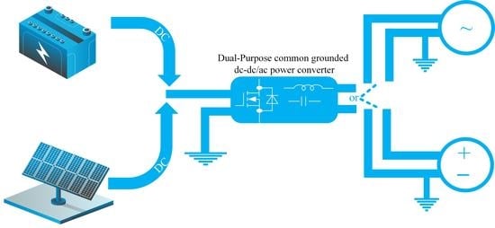
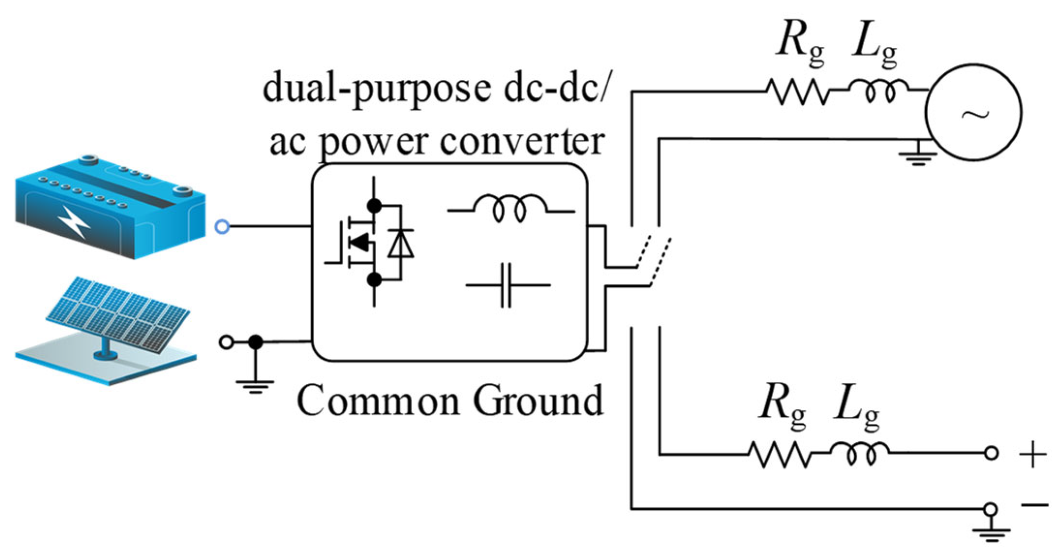
In light of the advantages of DC technology and the challenges associated with its implementation, it is believed that power electronic converters capable of functioning in both DC and AC applications could be a promising solution. The dual-purpose DC-DC/AC approach offers a means to minimize investment risks in DC infrastructure and provide greater flexibility for consumers. This concept is illustrated in Figure 1 and has been explored in several sources, including [9,10,11,12].
Design, implementation, and efficient operation of DC infrastructures are topics of discussion. They should be considered in dual-purpose DC-DC/AC power converters as well. One of the key issues to be taken into consideration is protection [13], and corrosion is one of its important aspects. It results from the electro-chemical process in a concrete structure such as a building. Concrete contains salt. The DC leakage current is conducted by metal and makes it anodic. The reaction between the anodic metal and the existing salt leads to the production of oxygen which makes the environment corrosive. Therefore, the metal slowly corrodes and dissolves the reinforcement. One solution to tackle leakage current is an earth leakage circuit breaker. This can switch off the installation if the leakage current reaches a certain value. In other words, if the leakage current stays below the specified value, the circuit breaker does not operate, and the metal reinforcement is in danger. Even several milliamperes of DC leakage current can create a corrosive environment. The damage of a DC leakage current is 100 times higher than the damage of an AC leakage current of the same size. Hence, using an earth leakage current circuit breaker is not an appropriate idea. Corrosion problems can be solved if leakage currents are prevented from flowing through the earthing facilities. In order to achieve this goal, sources are earthed indirectly through a capacitor diode network. The diodes block the leakage currents as long as the applied voltage remains below the diode voltage. The number of capacitor diode networks depends on the number of decentralized sources. In the case of several decentralized sources, a single ground point is not sufficient. This affects the system grounding configuration, and consequently a greater number of capacitor diode networks is required. Moreover, this solution is suitable for DC power systems. If the dual-purpose DC-DC/AC power converter operates in an AC power grid, another approach is required to suppress AC leakage. This burdens the system.
In most cases, there are numerous methods available for designing the grounding system in an electrical power network, and each of these approaches can lead to varying levels of performance outcomes [14]. It is important to note that the primary purposes of grounding are for identifying ground faults and ensuring the safety of personnel and equipment [15]. Low-Voltage (LV) DC microgrids can be grounded through high resistance or low resistance. The ground can be connected either to one of the poles or to the middle point if it is available. Low-resistance grounding means that the grounded wire has a very similar potential to AC grids. The opposite case in DC systems requires only high-resistance grounding and cannot eliminate leakage current, which in turn leads to corrosion problems.
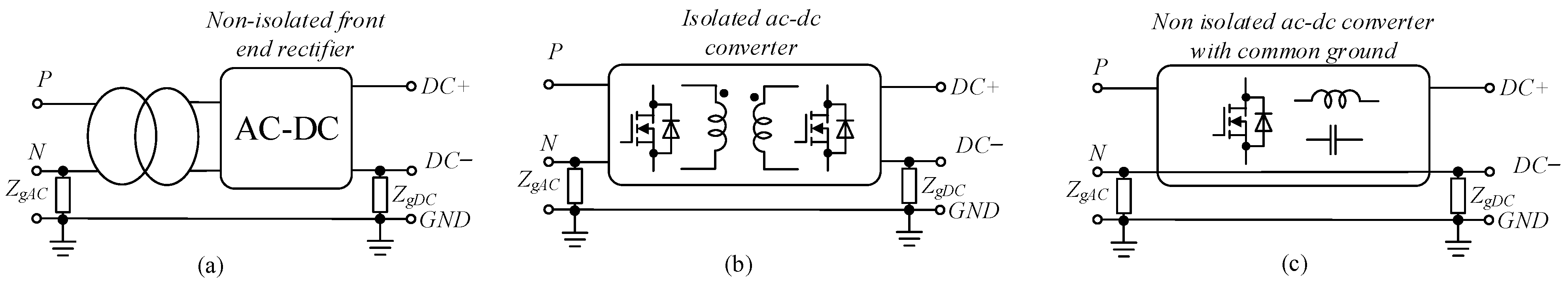
The way of grounding depends on the interconnection between AC and DC grids. Figure 2 shows different scenarios of DC grids where the grounding can be realized by low impedance on both sides. First of all, power flow between AC and DC microgrids can be provided by low-frequency transformers and non-isolated front-end rectifiers (Figure 2a). Figure 2b shows an isolated ac-DC converter. Finally, Figure 2c shows a non-isolated power electronics interface. The last solution does not have any redundancy. Moreover, it requires DC-AC energy conversion with common ground. The used transformers in the first two solutions impose a high volume to the system and decrease its efficiency. The common-ground architecture is a suitable approach for DC and AC systems in terms of full elimination of the DC and AC leakage currents. It could be a suitable candidate for dual-purpose DC-DC/AC power converters. Furthermore, such types of converter can be used as interfaces between DC and AC grids.
There are many DC-AC converters with common-ground architecture [16,17,18,19,20,21,22,23,24]. They also have the capability of dual-purpose DC-DC/AC operation. The Switched-Capacitor (SC) or Flying Capacitor (FC) solutions [16,17] and their derivatives [18] have common-ground features. However, they cannot realize a boost mode and suffer from inrush current.
Multilevel SC-based structures are presented in [19,20,21,22,23,24]. These structures can also inject power to the grid at an input voltage lower than the peak grid voltage; however, their main shortcoming is inrush currents. Moreover, their voltage-boosting factor is constant.
Meantime, several novel common-ground solutions suitable for dual-purpose application have been already presented [25,26,27].
The main goal of this work is to provide comparative analysis of common-ground solutions suitable for dual-purpose DC-DC/AC applications. Prior to previously presented dual-purpose solutions, the novel common-ground Flying Inductor (FI) DC-AC converter [28] is selected for design and experimental verification for dual-purpose application. The selected DC-DC/AC power converter is evaluated and compared with existing dual-purpose DC-DC/AC power converters.
The paper is organized as follows. Section 2 is devoted to the comparison between existing solutions. Section 3 describes the operation principle of the selected FI solution. Section 4 is devoted to the components’ design guidelines example. Section 5 is devoted to the prototype description and experimental verification. Finally, the main design challenges and conclusions are presented and discussed in Section 6 and Section 7, respectively.

2. Comparison Study

In this section, the aim is to compare dual-purpose DC-DC/AC power converters with common-ground features.
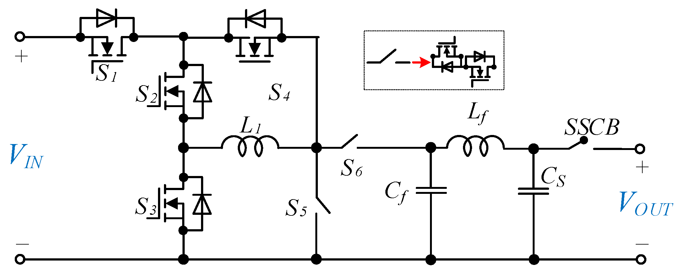
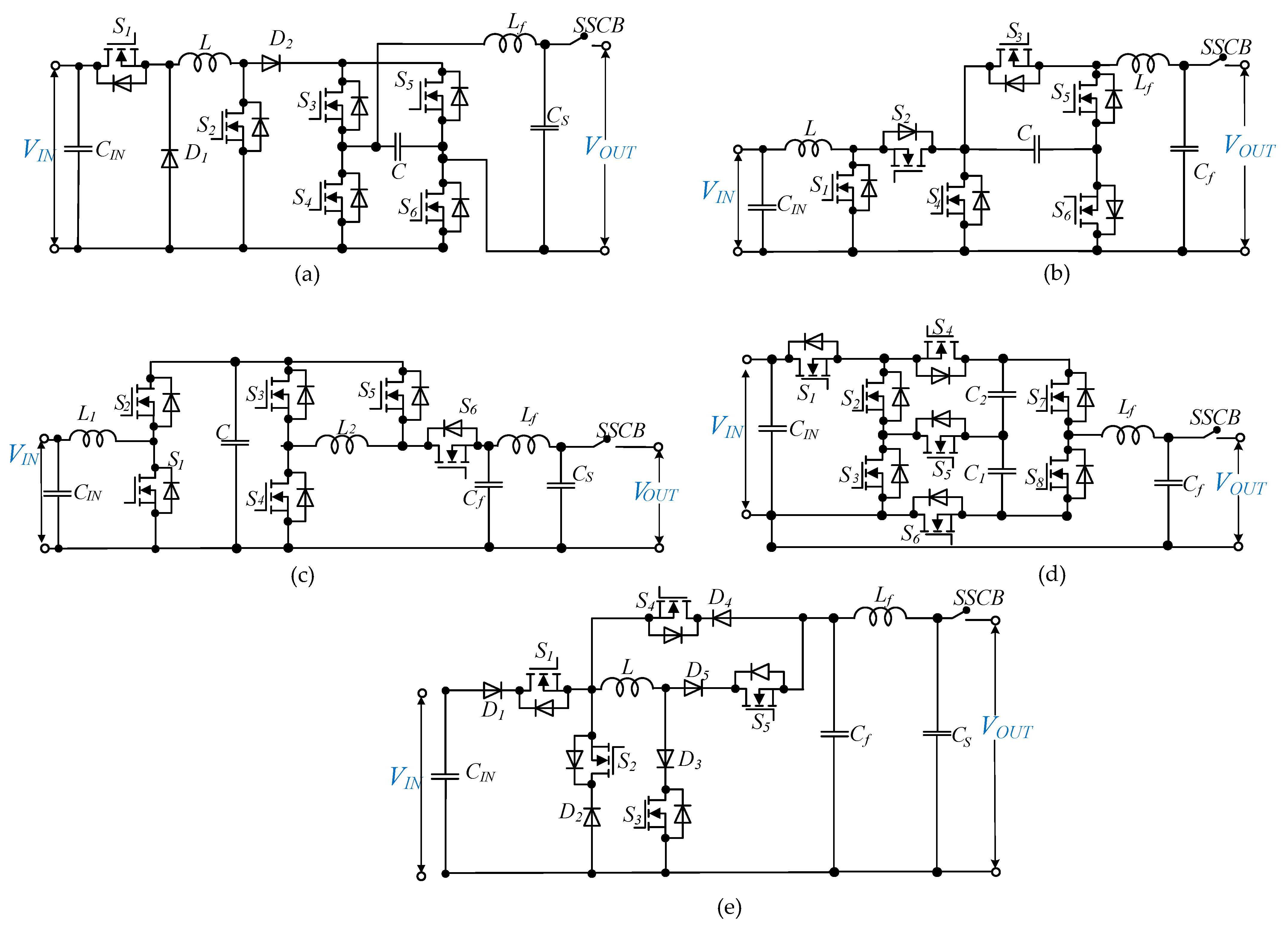
Figure 3 shows the circuit of an FI DC-AC converter presented in [28], as one of the novel family of FI inverters. By means of this example, we demonstrate that many solutions with additional suppressor capacitor CS and Solid-State Circuit Breakers (SSCB) for very fast disconnection in case of any emergency can be used for dual-purpose applications. It was shown in [9].
To compare different solutions for dual-purpose DC-DC/AC power conversion, the unfolding circuit with a buck–boost converter from [9] is used as a reference solution. Other options that are specifically designed for this purpose include the FC power converter in [25] and the FI-based power converter in [27]. In addition, many of the latest inverters and multilevel inverters are capable of operating in both DC-DC and DC-AC modes. For the purposes of comparison, the five-level SC-based inverter from [24] and the FI-based power converter from [29] are also evaluated. The schematics of these solutions are shown in Figure 4. All of the solutions are common ground, except for the buck–boost converter and the unfolding circuit from [9]. While the unfolding circuit can significantly reduce leakage current, it cannot eliminate it entirely.
In [25], a dual-purpose power converter is introduced. It is based on the FC circuit and operates as a three-level inverter. During DC-DC and DC-AC conversion, a capacitor is used to pump energy into the negative output voltage. On the other hand, the inverter in [24] is based on the SC circuit and uses two capacitors as voltage sources in the negative half cycle. Although the virtual voltage source concept is used in [24,25], they differ in terms of capacitor charging. In [25], the capacitor charges smoothly through a charging inductor, while in [24], the capacitors charge directly from the voltage source at the switching frequency, resulting in current spikes. In contrast, the unfolding circuit in [9] uses a virtual capacitor that functions as a current source.
Similar to the selected dual-purpose FI power converter, the introduced power converters in [27,29] are based on FI circuits, and the required energy is pumped from the inductors to the output. Among the compared topologies, the SC power converter in [24] has a fixed double-voltage boosting capability, while other solutions can operate under a wide range of input voltages.
It is aimed to discuss the advantages and disadvantages of each structure. To reach this goal, it is important to pay attention to the point that each structure is designed, built, and tested under different conditions; hence, it is not possible to make a fair comparison. However, the fundamental waveforms of a typical converter are independent of the component type and electric parameters (e.g., switching frequency and selected semiconductors). To put it differently, the primary wave forms are produced through the fundamental modulation method, which establishes certain overall requirements for component sizing. These requirements involve estimating passive component values, which can be achieved by considering equal current ripples in the inductors and identical voltage ripples across the capacitors.
In (1) and (2) the maximum accumulated energy inside a capacitor and an inductor are calculated, respectively. According to these equations, the volume of a core of an inductor as well as the volume of a capacitor can be estimated:
V o l C W C = i = 1 N C C i . v ^ C i 2
V o l L W L = i = 1 N L L i . i ^ L i 2
In (1), Ci and NC are the capacitance of the ith capacitor and the number of capacitors, respectively. Furthermore, v ^ C i represents the peak voltage of the ith capacitor. In (2), Li and NL are the inductance of the ith inductor and the number of inductors, respectively. In addition, i ^ L i is the peak inductor current.
The losses of conductivity in relation to the switch current are directly proportional to the square of the current, and are independent of semiconductors. Total conduction losses can be obtained by (3):
P C O N i = 1 N S i ˜ S i 2
Finally, we can estimate the Total Standing Voltage (TSV) across the semiconductors:
T S V i = 1 N S V ^ S i
Based on the above-mentioned points, we provided the same condition for all the selected topologies in the PSIM environment under equal conditions as the following.
The inductors were selected to have a current ripple equal to 20% of their current ratings. With this assumption, the used charging inductor in [9,25] is 3.3 mH, the two inductors in the flying inductor power converter in [27] are 1 mH, the inductor in the flying inductor power converter in [29] is 1.1 mH, and the inductor in the selected dual-purpose DC-DC/AC power converter is 1 mH.
The capacitors were selected to have a voltage ripple equal to 10% of their voltage ratings. With this assumption, the used capacitor is 10 uF in the FC-based power converter in [25], is 2 uF in the buck–boost and unfolding circuit in [9], is 300 uF in the FI-based power converter in [27], and is 1600 uF for C1 and 680 uF for C2 in the SC-based inverter in [24].
The output filter for the selected dual-purpose DC-DC/AC power converter, the FI-based power converter in [27], the FI-based power converter in [29], and the buck–boost and unfolding circuit in [9] is a CL type. The output filter for the FC-based power converter in [25] and the switched-capacitor inverter in [24] is a CL type. In all the compared topologies, the output filter capacitor is 3.3 uH. It should be noted that the used capacitor in the unfolding circuit acts as the output filter capacitor and is equal to 2 uF. There is no additional output filter capacitor in this topology. In the selected topology, the inductance of the output filter inductor is 500 uH. It results in 2.53% Total Harmonic Distortion (THD) in the output current. Hence, the output filter inductors are selected to have the same THD in the output current. Based on this assumption, the output filter inductor is 750 uH for the buck–boost and unfolding circuit in [9], is 1700 uH for the FC-based power converter in [25], is 1 uH for the FI-based power converter in [27], is 700 uH for the FI-based power converter in [29], and is 2000 uH for the SC-based power converter in [24].
The parameters in Table 1 were considered for all the compared topologies to simulate the same conditions.
The power switches in the circuit were assumed to have an on-state resistance of 0.028 Ω, which is the internal resistance of the NVHL020N120SC1 switch, a type of N-channel MOSFET power switch with a body diode. In contrast, the power switches used in a previous power converter design (referenced as [29]) were Insulated Gate Bipolar Transistor (IGBT) power switches without body diodes, which limit the current to flow in only one direction. MOSFETs, on the other hand, have bidirectional current flow capability inherently. To account for the unidirectional current flow in the IGBT-based design, a diode was added in series with the power switch in the simulation. For power diodes, the on-state resistance (Ron,D) was assumed to be 0.05 Ω, and the forward voltage (Vfw,D) was assumed to be 0.65 V in the circuit models.
The comparison between different circuit designs focused on several key factors, including the accumulated energy of capacitors (WC), the accumulated energy of inductors (WL), the Total Standing Voltage (TSV) of the semiconductors, conduction losses of the semiconductors (PCON), and the number of power switches used (NSW). It has been previously discussed in reference [25] that a smaller number of power switches does not necessarily result in higher efficiency, and this issue will also be explored in the current discussion.
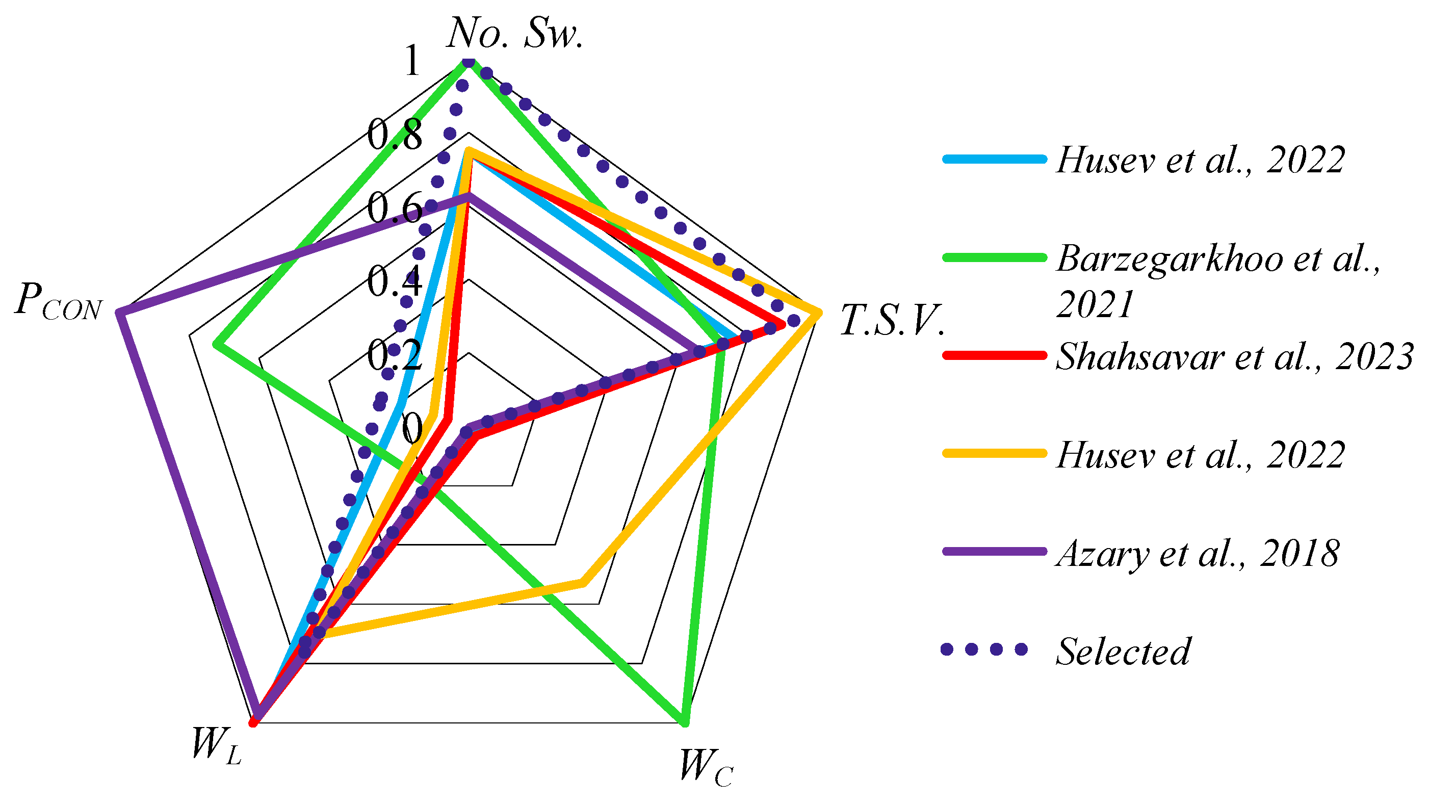
Figure 5 presents a radar chart comparing the different circuit topologies based on their calculated parameters shown in per unit values. The inverter introduced in reference [24] uses an SC circuit and has the highest capacitor value among the compared designs, resulting in high accumulated energy in the capacitors. However, this topology also has significant conduction losses. Switched-capacitor circuits are susceptible to current spikes that occur when the capacitors are being charged, causing inrush currents to pass through the power switches in the charging path, leading to higher current stress and power losses. As the output power increases, the magnitude of these current spikes becomes higher, potentially damaging the power switches. Therefore, SC-based solutions are not suitable for high-power applications. The FI power converter in [29] has the highest value of conduction losses due to power losses across the series-connected power diodes with the power switches. In contrast, the selected dual-purpose DC-DC/AC power converter, the FC-based power converter in [25], and the buck–boost unfolding circuit in [9] have the lowest accumulated energy in the capacitors. The selected dual-purpose DC-DC/AC power converter and the introduced power converter in [29] use FI architecture, and the filter capacitor is the only capacitor used in their configuration. The dual-purpose converters in [9,25] use a pseudo DC-link approach, which significantly reduces the capacitor size while maintaining good grid current quality. In terms of accumulated energy inside the inductors, the selected dual-purpose power converter stands out among the compared topologies, while the FI-based power converter introduced in [29] ranks highest. Regarding TSV, the introduced flying inductor dual-purpose converter in [27] has the highest voltage stress across its power switches.

3. Introduction to the Selected Solution Based on an FI Circuit

The topology selected for this study, as depicted in Figure 3, is based on a Flying Inductor (FI) circuit. The FI circuit operates by receiving and storing electrical energy from the input source at one point in time and delivering it to the output at another point in time, in a periodic switching cycle. One significant advantage of this topology is that it eliminates leakage current completely, by directly connecting the negative polarities of the input voltage source and the output side. This enhances the quality of power injected into the AC grid and improves system efficiency. To handle the bidirectional voltage stress on switches S5 and S6, a back-to-back combination of MOSFET switches is employed. Additionally, to minimize conduction losses on the input side, switch S1 is utilized instead of a diode and functions as an active diode. In comparison to a previously introduced FI-based topology [30], the selected converter’s inductor current is bidirectional under a DC-AC operating mode. Moreover, the converter’s buck–boost capability enables power injection into the output grid over a broad range of DC input voltages.
The bi-directional nature of the selected dual-purpose DC-DC/AC power converter is especially valuable for energy storage systems that rely on batteries. It is particularly useful for home-scale storage systems that can charge batteries during low-consumption periods of the grid and discharge the stored energy into the grid during peak consumption periods using the selected dual-purpose DC-DC/AC power converter. The operation of the selected converter is examined below in both DC-AC and DC-DC modes.

3.1. Buck–Boost Operation Mode

In more technical terms, the selected dual-purpose DC-DC/AC power converter is capable of operating in two modes: buck–boost and buck. The buck–boost mode, which is characterized by symmetrical operation states, allows the converter to operate independently of the input voltage. This mode involves the storage of energy in the FI L1 during one time period, followed by the injection of this energy into the output filter and the grid during another time period. This cycle repeats periodically, ensuring a continuous flow of power.
  • Positive output voltage generation:
When the output voltage is positive, the selected dual-purpose DC-DC/AC power converter operates in two equivalent circuits, as shown in Figure 6a,b. In the first circuit, switches S1, S2, and S5 are turned on to allow current to flow through the input source and charge inductor L1, while the other switches are turned off. The output filter Lf’s current flows through capacitor Cf, creating a free-wheeling mode in the positive half cycle. The bi-directional SSCB switch remains operational in all modes, disconnecting the converter from the grid side in case of system errors to prevent voltage spikes. In the second circuit, switches S3 and S6 are turned on to transfer the stored energy in inductor L1 to the output filter and the grid, while other switches are off.
  • Negative output voltage generation:
To generate a negative output voltage, the buck–boost mode is employed in the selected power converter. In this mode, the direction of the current in inductor L1 is opposite to that of the positive output voltage generation. Switches S1, S3, and S4 are turned on, providing a charge path for L1. The current of the output filter Lf flows through the capacitor Cf. The equivalent circuit for this mode is depicted in Figure 6c.
The second equivalent circuit in case of negative output voltage generation is shown in Figure 6d. It can be called the active mode when switches S3 and S6 are turned on, and the stored energy in inductor L1 is pumped to the output.
In the selected converter, the currents of switches S3 and S6 are bidirectional, while the current of other switches is unidirectional. Furthermore, the charging path of inductor L1 is shown by a blue line in operating modes and the output current path is shown by a red line.

3.2. Buck Operation Mode

The selected converter has flexibility in the case of positive output voltage generation. It depends on the value of input voltage. If the input voltage is less than the output voltage, the operating modes of the converter will still be the same as in the buck–boost mode, which is that described in Figure 6a,b. However, when the value of the input voltage is greater than the instantaneous value of the output voltage, then the converter will operate in the buck mode. The first equivalent circuit of the buck mode is shown in Figure 7a. In this mode, unlike in the buck–boost state, the inductor L1 is used as a filter. This causes the current of inductor L1 to be less in the positive output voltage generation than in the negative half cycle. In this case, switches S1, S2, and S6 are conducting, and S4 and S5 are completely off. The second equivalent circuit of the second operating mode is shown in Figure 7b. In this case, switch S2 turns off and switch S3 turns on. In other words, switch S3 acts as a freewheeling switch. Furthermore, in this mode, although the current of switch S1 is zero, the pulse of this switch is still established. If the input DC voltage is higher than the peak value of output voltage, then only the buck mode can be utilized.
From that written above, it is possible to conclude that in the DC-AC mode, the converter can be operated in both buck–boost and buck modes, which depend on the value of the input voltage. In the DC-DC mode, if a positive voltage is required at the output terminals, the operating modes will be the same as in Figure 6a,b. Furthermore, if a negative voltage is required at the output, then the operating modes of the selected converter will be the same as in Figure 6c,d. Since the negative terminals at the input and output are interconnected, it is best to use a positive polarity in the DC-DC mode as in Figure 6a,b. Due to the symmetrical shape of the inductor current, the buck–boost mode can be called a symmetrical mode, while the combination of buck and buck–boost can be called asymmetrical.

4. Passive and Active Component Design Guidelines

In this section, the values of active and passive elements are designed. The used switches are selected based on the rate of voltage and current stress. In addition, the value of passive elements is calculated based on the amount of output power.

4.1. Design of the Flying Inductor L1

In this section, the value of the FI L1 is designed. The volt-second balance rule is applied for inductor L1 to calculate the inverter switching duty cycles as follows:
d ( t ) = v C f v C f + V I N
In (5), VIN and Vcf refer to the input voltage, and the voltage across output filter capacitor is Cf. The output filter inductor has a smaller value; hence, the voltage drop across this inductor is small at the grid frequency, causing the capacitor voltage Cf (VCf) to be almost equal to the output voltage. The output voltage is also expressed as follows:
v o u t ( t ) = V o , max sin ω t
In the above relation, Vo,max is the peak output voltage. By considering the equality of the output voltage and Vcf, and substituting (6) into (5), the inverter switching duty cycle is expressed as follows under the buck–boost mode:
d ( t ) = V o , max sin ω   t V o , max sin ω   t + V I N
The charging and discharging time of inductor L1, defined by Ton and Toff, is calculated as follows:
T o n = d ( t ) f S = V o , max sin ω   t f S V o , max sin ω   t + V I N
T o f f = 1 V o , max sin ω   t f S V o , max sin ω   t + V I N
Here, fS and TS are the switching frequency and switching time period of the inverter, respectively. The current ripple of inductor L1 is expressed as follows:
Δ I L 1 = 1 L 1 0 d T S v L 1 d t    
Taking d(t) from (7) and substituting it into (10), the inductance value of L1 is obtained as follows:
L 1 =   V o , max V I N sin ω   t Δ I L 1 f S V o , max sin ω   t + V I N
Given that the maximum ripple current of inductor L1 occurs at the peak voltage of the grid, the value of the inductor L1 is expressed as follows based on the maximum ripple current:
L 1 = V o , max V I N Δ I L 1 , max f S   V o , max + V I N
The value of inductor L1 in (12) is rewritten in (13) according to the average value of output power Pout, the average input voltage, the peak of output voltage, and the switching frequency, as follows:
L 1 = V 2 o , max V 2 I N f S P o u t   V o , max + V I N 2

4.2. Design of the Output Filter Inductor and Capacitor

The equation of the output load current or AC grid current in the unity power factor is expressed by the following relation:
i o u t ( t ) = I o , max sin ω t
During Ton, inductor L1 is charged from the input source and the current of the filter Lf passes through capacitor Cf. Therefore, the voltage ripple of this capacitor is expressed as follows:
Δ V C f = 1 C f 0 T o n I o , max sin ω t   d t = I g , max C f ω 1 cos ω T o n
Δ V C f = I g , max C f ω 1 cos ω T o n
By applying relation (8) to (16) and simplifying it, the capacitance of capacitor Cf can be calculated as follows:
C f = 2 P o u t 2 π f g Δ V C f V o , max 1 cos 2 π f g V o , max sin ω t f S V o , max sin ω t + V I N
Since the maximum voltage ripple of capacitor Cf occurs at the peak voltage of output, the capacity of this capacitor can be calculated based on the maximum voltage ripple, as follows:
C f = 2 P o u t 2 π f g Δ V C f V o , max 1 cos 2 2 π f g V r m s f S 2 V r m s + V I N
The value of the Lf filter inductor can be obtained based on the cut-off frequency of the output filter. For this purpose, the following relationship is established:
L f = 1 C f 2 π f C 2
In the above, fc is the corner frequency of the output filter.

4.3. Current and Voltage Stress of the Selected Topology

In the selected converter, at time Ton, inductor L1 is charged from the input source and delivers its energy to the output at the Toff interval. A part of the switches charges this inductor from the input source and another part discharges it by transferring energy to the output. Therefore, in this topology, all switches have the same current stress equal to the current passing through inductor L1. The current equation of inductor L1 based on the output current and the value of the switching duty cycle is expressed as follows:
i L 1 ( t ) = 1 1 d ( t ) i o ( t ) + Δ i L 1 ( t ) 2
The maximum duty cycle occurs at the peak output voltage and is expressed as follows:
D max = V o , max V o , max + V I N
Therefore, the peak current of inductor L1 is determined based on the peak value of output current, maximum ripple current, and maximum duty cycle, as follows:
I L 1 , p e a k = 2 V I N + V o , max P o u t V I N V o , max + V o , max V I N 2 L 1 f S   V o , max + V I N .
I L 1 , p e a k = 4 L 1 f S V I N + V o , max 2 P o u t + V 2 o , max V 2 I N 2 L 1 f S V I N V o , max   V o , max + V I N
The stress of all switches is equal to Equation (24). The voltage stress of the switches varies. For example, as long as the input voltage is less than the peak value of output voltage, then the voltage stress of switch S1 is as follows:
V S 1 = V o , max V I N
In addition, if the input voltage is higher than the peak value of output voltage, then the internal diode of switch S1 is always conducting and the voltage of this switch is zero. The voltage stress of other switches is also given below:
V S 2 = V S 5 = V o , max
V S 3 = V I N
V S 4 = V S 6 = V I N + V o , max

5. Experimental Verification

In this section, a number of experimental results of the selected converter are presented in order to evaluate its performance. The active and passive device components used in the practical results section are shown in Table 2.
The value of inductor L1 is also obtained from Equations (12) and (13) by considering the appropriate current ripple. The TMS320F28379D microcontroller is specifically designed for power electronic applications and features 24 Pulse Width Modulation (PWM) channels and four Analogue to Digital Converters (ADCs) with the ability to handle up to 12 external channels. Its primary function in this context is to control switches and SSCB relay and generate PWM pulses. If the selected topology’s requirements in terms of PWM and ADC channels can be met by a less expensive microcontroller, it can be substituted. The control system used for this converter is a Model Predictive Control (MPC) that has been investigated in a previous study (reference [31]). The input voltage source is a PV simulator type, which allows testing of the converter under real conditions when connected to a solar panel system. Experimental results have been obtained for both DC-AC and DC-DC modes. A laboratory prototype of the selected converter is shown in Figure 8. The converter has buck–boost capability, enabling it to operate over a wide range of input voltages, typically ranging from 100 to 400 V. In DC-AC mode, the output voltage is 230 V RMS, while in DC-DC mode, it is 350 V.
When operating in the buck or asymmetric mode, as shown in Figure 7, the current of inductor L1 is smaller than in the symmetric or buck–boost mode when the output power is held constant. This is primarily due to direct energy transmission from the input source to the output, with inductor L1 acting as a filter. In the symmetric or buck–boost mode, energy is first stored in inductor L1 and then delivered to the output, resulting in a higher inductor L1 current. As a result, the system efficiency is better in the asymmetric mode than in the symmetric mode, and the experimental results are therefore discussed more in the context of an asymmetric mode.

5.1. DC-AC Mode

The objective in the DC-AC mode is to produce a sinusoidal AC voltage at the converter’s output terminals, regardless of a wide range of variations in the input DC voltage. Figure 9a depicts the input current (Idc), FI current ( I L 1 ), input voltage (Vdc), and output voltage (VOUT) from top to bottom. The figure shows that the input voltage is 200 V DC, while the output voltage is 230 V RMS, with an output power of 1.5 kW.
As shown in this figure, the dual-purpose DC-DC/AC power converter operates in buck mode when the output voltage’s instantaneous value is less than the input voltage value, and it switches to buck–boost mode when the output voltage’s instantaneous value is greater than the input voltage value. From Figure 9a, it is evident that the current of inductor L1 is not symmetrical in the positive and negative half cycles. However, despite this asymmetry in the inductor current, the output voltage remains symmetrical.
Figure 9b displays Idc, I L 1 , Vdc, and VOUT per 2 kW output power. In this figure, the converter’s applied voltage is 400 V. As the input voltage is higher than the output voltage’s peak value, the dual-purpose DC-DC/AC power converter operates in buck mode during the positive half cycle and buck–boost mode during the negative half cycle. Inductor L1 acts as a filter during the positive half cycle, causing the current in this interval to be lower than that in the negative half cycle. Figure 9b also demonstrates that the input current in the positive half cycle is lower than that in the negative half cycle. Nevertheless, despite the asymmetric performance of the converter, the output voltage remains perfectly symmetrical. The converter’s efficiency can be enhanced by reducing the current in the positive half cycle or making the converter operate asymmetrically.
Figure 9c illustrates Idc and I L 1 at the moment when the converter changes from buck–boost to buck mode. As indicated by the figure, the input current ripple and inductor current L1 are lower in buck mode than in buck–boost mode. Moreover, the converter’s operation switches without a transient state, as demonstrated in the figure. Despite this change, the output voltage remains sinusoidal.

5.2. DC-DC Mode

This section discusses the experimental results of the selected converter in the DC-DC operation mode. The selected converter has a buck–boost capability, which enables it to operate over a wide range of input voltages. The objective is to generate a 350 V output DC voltage while varying the input voltage between 200 V and 400 V. The converter can produce both positive and negative polarity voltage at the output, but generating positive polarity voltage is preferred as the converter can also operate in the buck mode, leading to improved efficiency. Moreover, generating positive polarity voltage creates a common connection between the input and output terminals.
The information presented in Figure 10a illustrates the input current (Idc), FI current ( I L 1 ), output voltage (VOUT), and the input voltage (Vdc), from top to bottom. The input voltage depicted in this figure is 200 V, whereas the output voltage is 350 V, indicating that the power converter selected for this demonstration is in buck–boost mode with a duty cycle exceeding 0.5, as discernible from the waveform of inductor L1 current. Moreover, this figure shows that the output power is 2 kW. Figure 10b shows Idc, I L 1 , VOUT, and Vdc from top to bottom, respectively. In this figure, the input voltage is equal to 400 V and the output voltage is 350 V in its previous value. In addition, the output power is 2 kW. Due to the fact that in this figure the input voltage is more than the output voltage, the selected dual-purpose DC-DC/AC power converter operates under the buck mode. In this case, the duty cycle needs to be around 0.875. The L1 inductor current ripple verifies this issue. The performance of the selected converter at higher power is demonstrated in Figure 10c. At this level, the output power is approximately 4 kW, and the input voltage is 400 V. Similar to Figure 10b, the converter functions in buck mode in Figure 10c due to the output voltage being lower than the input voltage.
Based on the information presented in Figure 10, it can be inferred that the selected dual-purpose DC-DC/AC power converter has the capability to generate a constant DC voltage on the output terminal, even with a variable input voltage. This converter topology can be employed in DC grids. The selected converter utilizes two four-quadrant switches, and precise adjustment of the dead time is necessary in these switches. For instance, during the positive half cycle, the dead time must be accurately set between switches S5 and S6, and during the negative half cycle, it should be precisely adjusted between switches S4 and S6. Failure to fine-tune the dead time between the switches can result in increased losses and voltage spikes in the switches.
Figure 11a,b depicts the voltage stress on switch S4, current stress of inductor L1, and voltage stress on switches S5 and S6, respectively, from top to bottom. In Figure 11a, the dead time between the switches is appropriately adjusted, resulting in an acceptable voltage spike across the switches. Lower voltage spikes across the switches aid in reducing switching losses. In contrast, in Figure 11b, the dead time between the switches is not correctly adjusted. This leads to an increased voltage spike in the switches, resulting in higher switching losses. Additionally, an incorrect dead-time setting between the switches may cause the switches to malfunction, owing to the high voltage spikes. Figure 11c demonstrates the performance of the chosen converter during output power step changes. In this instance, the input voltage is 400 V, and the converter is in buck–boost or symmetrical operation mode. The output power has risen from 1 kW to 2 kW with the increase in load, doubling the input and inductor L1 current values. From Figure 11c, it is evident that the output voltage remains stable at the time of output load step changes, indicating that the converter can handle these conditions effectively.
Figure 12 is presented to demonstrate the performance of the chosen dual-purpose DC-DC/AC power converter under step-change conditions. The aim is to produce a step change in the peak output voltage, while the input voltage remains constant at 200 V. In Figure 12a, a step change is implemented in the reference value of the output voltage, with the intention of increasing the peak output voltage from 220 V to 325 V. As depicted in the figure, the output voltage follows the step change, and the output voltage of the selected converter remains stable. Furthermore, the output power increases from 0.5 kW to 1 kW in this figure. In Figure 12b, unlike Figure 12a, the objective is to decrease the peak value of the output voltage. In this figure, a step change is implemented at the output voltage, resulting in a reduction of the peak value of the output voltage from 325 V to 220 V. Additionally, the output power decreased from 1 kW to 0.5 kW. Figure 12c depicts I L 1 , output current (IOUT), Vdc, and VOUT from top to bottom, respectively. The input voltage is 400 V, and the output power is 1.5 kW. This figure is presented to illustrate the operation of the chosen converter in transient mode, from symmetric to asymmetric modes and vice versa. The symmetric and asymmetric operating modes are determined based on the flying inductor current value. As demonstrated in the figure, the output voltage remains constant in both symmetric and asymmetric operating modes. In other words, the control system maintains the output voltage at its nominal value.
The purpose of Figure 13a,b is to demonstrate the capability of the selected converter to control reactive power. This figure displays I L 1 , Vdc, VOUT, and IOUT when operating at leading and lagging power factors. It can be concluded from the figure that the dual-purpose DC-DC/AC power converter can effectively function at power factors other than unity. Figure 13c illustrates the voltage stress experienced by switches S1 to S3 in the converter. The input voltage is set at 200 V in this figure. It can be observed that the correct dead time between the switches has been set, as the spike voltage of the switches appears to be within normal range.
Figure 14a shows the input current, flying inductor current, input voltage, and output voltage from top to bottom, respectively. The purpose of this figure is to show the input voltage changes and to keep the output voltage constant for these changes. In Figure 14a, the converter’s input voltage is raised from 200 V to 400 V. The output voltage remains constant despite the increase in input voltage. This figure portrays how the control system operates when the input voltage changes while maintaining a constant output voltage. Additionally, the output power is maintained at 1 kW, which leads to a decrease in both the input current and flying inductor current as the input voltage increases. Figure 14b demonstrates that even when the input voltage is lowered from 400 V to 200 V, the control system maintains a constant output voltage. Moreover, since the output power is held constant at 1 kW in this figure, the reduction in input voltage causes an increase in both the input current and the flying inductor current. Figure 14c displays the output current, flying inductor current, input voltage, and output voltage in response to changes in output power. In this figure, the input voltage is 400 V, and the output power is increased from 1 kW to 2 kW. The figure indicates that increasing the output power from 1 kW to 2 kW results in an increase in both the output current and flying inductor current, while keeping the output voltage constant at its previous value.

6. Main Design Challenges

This section is devoted to the feasibility study of the selected converter for experimental verification. The unique feature of the FI power converter is that it has a continuous current in the inductor-charging path, unlike SC and FC power converters where the capacitor charge current is discrete. This requires the availability of a path to allow the inductor current to flow. Therefore, the biggest challenge in an FI converter is to ensure a smooth transition between the switches, which can be achieved through appropriate tuning of the dead time. This issue becomes more complicated when using a four-quadrant power switches arrangement, where the anti-parallel diode of each power switch is blocked by the other power switch.
If the dead time between the switches is too high, the inductor current will be obstructed for a brief period, leading to a substantial voltage surge across the switches. This surge will increase switching losses, decrease efficiency, and may harm the switches. To avoid this voltage spike issue, a snubber capacitor and varistor can be used as a solution, but this will add extra components, increase costs, and create additional losses. When the dead time between the switches is too low, the power switches will be in the on state, creating a quasi-short circuit. Although this limits the voltage surge across the switches, it also increases conduction losses and reduces efficiency, resulting in an increase in input current. Therefore, it is important to balance conduction losses and switching losses by finding an optimal dead-time value. This can be achieved by setting the dead time to different values and measuring efficiency using a power analyzer. Once the optimal point is found, the microcontroller can be used to adjust the dead time to the exact value.
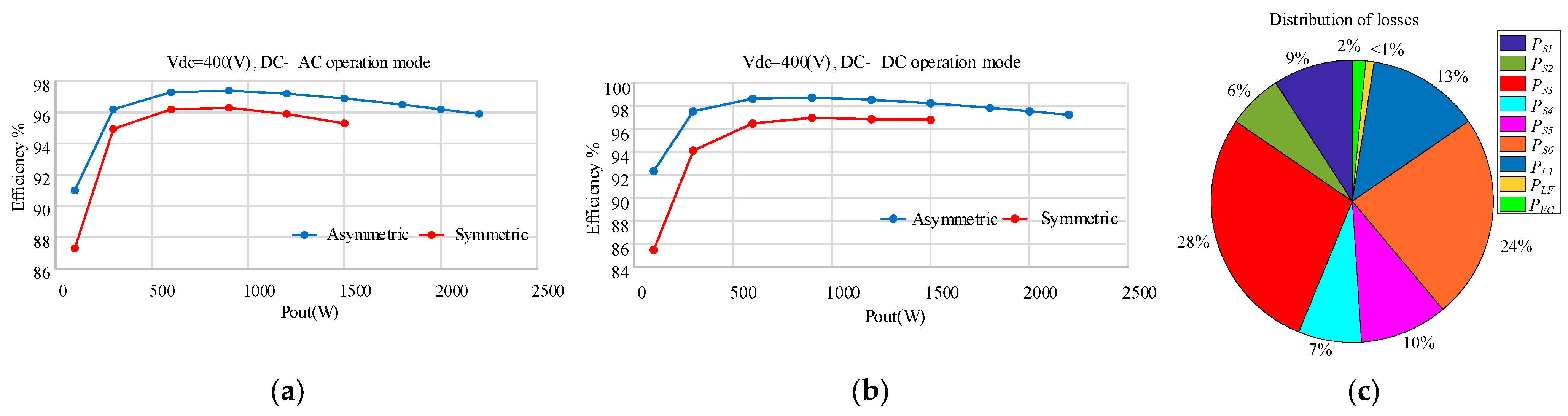
The efficiency curve of the dual-purpose DC-DC/AC power converter operating in DC-AC mode with a 400 V input voltage is depicted in Figure 15a. The efficiency diagram is presented in two modes: buck–boost (symmetric) and buck (asymmetric). From the figure, it is evident that the efficiency is higher in the buck mode compared to the buck–boost mode. By examining Figure 15a, it is apparent that the maximum efficiency for an output power of 0.8 kW is 97.5% in buck mode and 96.4% in buck–boost mode. In addition to Figure 15a, Figure 15b depicts the efficiency curves of the selected converter in DC-DC operating mode with a 400 V input voltage. It is evident from this figure that the maximum efficiency at an output power of 1 kW is approximately 98.6% for the buck operation state and about 97% for the buck–boost mode.
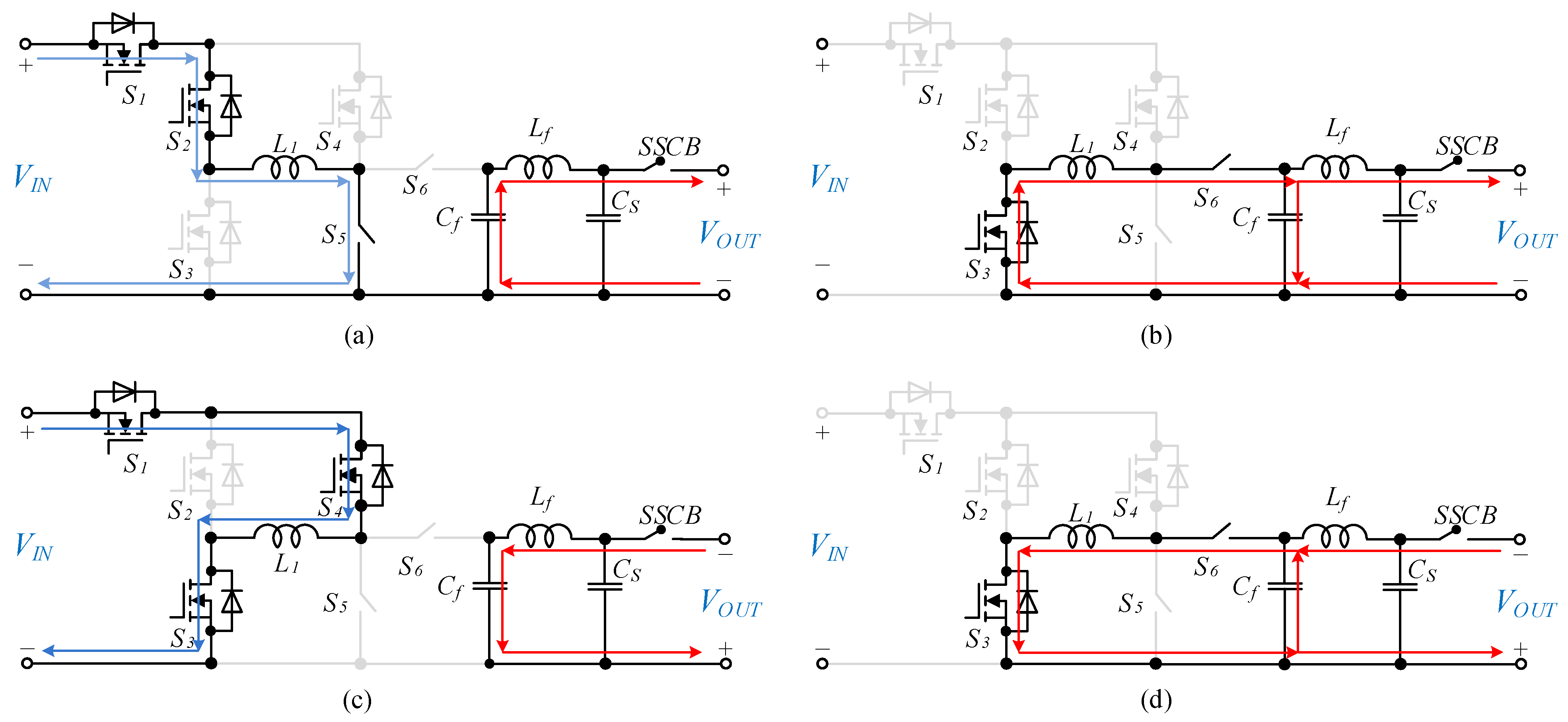
The recorded efficiency was based on the proper dead-time tuning. According to Figure 6, during the positive half cycle, the inductor undergoes a charging process via S5 and a discharging process via S6. In contrast, during the negative half cycle, the charging and discharging of the inductor are conducted through S4 and S6, respectively. To ensure that the current in the inductor is continuous while transitioning between the charging and discharging modes, it is imperative to establish an appropriate dead time between S5 and S6 and between S4 and S6. However, since the SiC power switches have inherent delays, as well as additional delays imposed by the gate driver, a dead time of zero is optimal for these mentioned power switches. On the other hand, the optimum dead time between other power switches has been determined to be 180 nS.
Figure 15c displays a pie chart indicating the percentage of losses for each converter element. The power losses of power switches are the sum of PCON (as written in (3)), and the switching losses (PSW) in (28) in which IS and Vs indicate the current and voltage stress of ith power switch, and N is the number of the used power switches. The conduction losses of the used inductors and the output filter capacitor are written in (29) and (30), respectively. In these equations, ESRL, Irms,L, ESRC, and Irms,C refer to the Equivalent Series Resistance of an inductor, RMS current of an inductor, the Equivalent Series Resistance of the filter capacitor, and RMS current of the filter capacitor, respectively. Table 3 gives additional information to calculate the power losses of each component.
P S W i = 1 N S i ^ S i . v ^ S i T .
P C o n , L = E S R L × I 2 r m s , L .
P C o n , C = E S R C × I 2 r m s , C .

7. Conclusions

In this paper, common-ground architecture was considered as a suitable solution for leakage current suppression in dual-purpose DC-DC/AC power converters. A comparative analysis was performed between several dual-purpose common-ground DC-DC/AC power converters. The comparison methodology was described comprehensively and the results were shown in the format of a radar chart illustrating the per unit values of WC, WL, TSV, PCON, and NSW of each structure. Each solution has pros and cons. At the same time, FI solutions have significant magnetics but small capacitors due to the single-stage conversion.
A recently introduced power converter, as a family of novel FI power converters, was selected to be discussed as a dual-purpose DC-DC/AC common-ground solution with experimental verification. It uses a FI to store energy and pumps it to the output and is capable of operating as a buck and buck–boost converter. The operating modes were analyzed and the components design was discussed. In order to evaluate and show the accuracy of the selected converter, the experimental results in DC-DC and DC-AC modes were presented and analyzed. Finally, the design challenges in the selected topology were considered, and the efficiency and the loss distribution were analyzed. As a conclusion, the research team recommends solutions presented in [9,25,27] for practical applications due to the absence of four-quadrant switches and decent figure of merit.

Author Contributions

Conceptualization, N.V.K. and O.H.; Methodology, T.H.S.; Software, O.M.; Validation, S.R., A.F. and O.M.; Formal analysis, T.H.S.; Investigation, S.R.; Resources, T.H.S.; Data curation, A.F.; Writing—original draft, T.H.S.; Writing—review & editing, O.H. and D.V.; Visualization, N.V.K.; Supervision, O.H.; Project administration, O.H.; Funding acquisition, D.V. All authors have read and agreed to the published version of the manuscript.

Funding

This work was supported by the Estonian Research Council grant PRG675. Work of D. Vinnikov was supported by the Estonian Research Council grant PRG1086.

Data Availability Statement

The data used in this study are publicly available and sources are referred.

Conflicts of Interest

The authors declare no conflict of interest.

References

  1. Novosel, D. More Power to the Future: Industry Trends in Electrical Power and Energy. IEEE Power Energy Mag. 2018, 16, 16–22. [Google Scholar] [CrossRef]
  2. Nan, J.; Yao, W.; Wen, J. Energy Storage-based Control of Multi-Terminal DC Grid to Eliminate the Fluctuations of Renewable Energy. J. Eng. 2019, 16, 991–995. [Google Scholar] [CrossRef]
  3. Zhang, L.; Sun, K.; Xing, Y.; Feng, L.; Ge, H. A Modular Grid Connected Photovoltaic Generation System Based on DC Bus. IEEE Trans. Power Electron. 2011, 26, 523–531. [Google Scholar] [CrossRef]
  4. Madduri, P.A.; Rosa, J.; Sanders, S.R.; Brewer, E.A.; Podolsky, M. Design and Verification of Smart and Scalable DC Microgrids For Emerging Regions. In Proceedings of the 2013 IEEE Energy Conversion Congress and Exposition, Denver, CO, USA, 15–19 September 2013; pp. 73–79. [Google Scholar]
  5. Lee, J.; Han, B.; Choi, N. DC Micro-Grid Operational Analysis with Detailed Simulation Model for Distributed Generation. In Proceedings of the 2010 IEEE Energy Conversion Congress and Exposition, Atlanta, GA, USA, 12–16 September 2010; pp. 3153–3160. [Google Scholar]
  6. Sannino, A.; Postiglione, G.; Bollen, M.H.J. Feasibility of A DC Network for Commercial Facilities. IEEE Trans. Ind. Appl. 2003, 39, 1499–1507. [Google Scholar] [CrossRef]
  7. Boroyevich, D.; Cvetkovic, I.; Dong, D.; Burgos, R.; Wang, F.; Lee, F. Future Electronic Power Distribution Systems a Contemplative View. In Proceedings of the 12th International Conference on in Proceedings of Optimization of Electrical and Electronic Equipment (OPTIM), Brasov, Romania, 20–22 May 2010; pp. 1369–1380. [Google Scholar]
  8. Carvalho, E.L.; Blinov, A.; Chub, A.; Emiliani, P.; de Carne, G.; Vinnikov, D. Grid Integration of DC Buildings: Standards, Requirements and Power Converter Topologies. IEEE Open J. Power Electron. 2022, 3, 798–823. [Google Scholar] [CrossRef]
  9. Husev, O.; Matiushkin, O.; Vinnikov, D.; Roncero-Clemente, C.; Kouro, S. Novel Concept of Solar Converter with Universal Applicability for DC and AC Microgrids. IEEE Tran. Ind. Electron. 2022, 69, 4329–4341. [Google Scholar] [CrossRef]
  10. Husev, O.; Vinnikov, D.; Kouro, S.; Blaabjerg, F.; Roncero-Clemente, C. Dual-Purpose Converters for DC or AC Grid as Energy Transition Solution: Perspectives and Challenges. IEEE Ind. Electron. Mag. 2023. early access. [Google Scholar] [CrossRef]
  11. Husev, O.; Matiushkin, O.; Jalakas, T.; Vinnikov, D.; Kurdkandi, N.V. Comparative Evaluation of Dual-Purpose Converters Suitable for Application in dc and ac Grids. IEEE J. Emerg. Sel. Top. Power Electron. 2023. early access. [Google Scholar] [CrossRef]
  12. Roncero-Clemente, C.; Husev, O.; Matiushkin, O.; Escalona, J.; Barrero-González, F.; Vinnikov, D.; Strzelecki, R. Feasibility Study of Three-Phase Modular Converter for Dual-Purpose Application in DC and AC Microgrids. IEEE J. Emerg. Sel. Top. Power Electron. 2023. early access. [Google Scholar] [CrossRef]
  13. Salomonsson, D.; Soder, L.; Sannino, A. Protection of Low-Voltage DC Microgrids. IEEE Trans. Power Deliv. 2009, 24, 1045–1053. [Google Scholar] [CrossRef]
  14. Paul, D. DC traction power system grounding. IEEE Trans. Ind. Appl. 2002, 38, 818–824. [Google Scholar] [CrossRef]
  15. IEEE Std. 946-2004; IEEE Recommended Practice for the Design of DC Auxiliary Power Systems for Generating Stations. IEEE: Piscataway, NJ, USA, 2004.
  16. Gu, Y.; Li, W.; Zhao, Y.; Yang, B.; Li, C.; He, X. Transformerless Inverter with Virtual DC Bus Concept for Cost-Effective Grid-Connected PV Power Systems. IEEE Trans. Power Electron. 2013, 28, 793–805. [Google Scholar] [CrossRef]
  17. Ardashir, J.F.; Sabahi, M.; Hosseini, S.H.; Blaabjerg, F.; Babaei, E.; Gharehpetian, G.B. A Single-Phase Transformerless Inverter with Charge Pump Circuit Concept for Grid-Tied PV Applications. IEEE Trans. Ind. Electron. 2017, 64, 5403–5415. [Google Scholar] [CrossRef]
  18. Siwakoti, Y.P.; Blaabjerg, F. Common-Ground-Type Transformerless Inverters for Single-Phase Solar Photovoltaic Systems. IEEE Trans. Ind. Electron. 2018, 65, 2100–2111. [Google Scholar] [CrossRef]
  19. Barzegarkhoo, R.; Siwakoti, Y.P.; Blaabjerg, F. A New Switched-Capacitor Five-Level Inverter Suitable for Transformerless Grid-Connected Applications. IEEE Trans. Power Electron. 2020, 35, 8140–8153. [Google Scholar] [CrossRef]
  20. Barzegarkhoo, R.; Siwakoti, Y.P.; Vosoughi, N.; Blaabjerg, F. Six-Switch Step-Up Common-Grounded Five-Level Inverter with Switched-Capacitor Cell for Transformerless Grid tied PV Applications. IEEE Trans. Ind. Electron. 2021, 68, 1374–1387. [Google Scholar] [CrossRef]
  21. Vosoughi, N.; Hosseini, S.H.; Sabahi, M. A New Transformer-Less Five-Level Grid-Tied Inverter for Photovoltaic Applications. IEEE Trans. Energy Convers. 2020, 35, 106–118. [Google Scholar] [CrossRef]
  22. Shaffer, B.; Hassan, H.A.; Scott, M.J.; Hasan, S.U.; Town, G.E.; Siwakoti, Y. A Common-Ground Single-Phase Five-Level Transformerless Boost Inverter for Photovoltaic Applications. In Proceedings of the 2018 IEEE Applied Power Electronics Conference and Exposition (APEC), San Antonio, TX, USA, 4–8 March 2018; pp. 368–374. [Google Scholar]
  23. Samizadeh, M.; Yang, X.; Karami, B.; Chen, W.; Blaabjerg, F.; Kamranian, M. A New Topology of Switched Capacitor Multilevel Inverter with Eliminating Leakage Current. IEEE Access 2020, 8, 76951–76965. [Google Scholar] [CrossRef]
  24. Barzegarkhoo, R.; Lee, S.S.; Khan, S.A.; Siwakoti, Y.P.; Lu, D.D. A Novel Generalized Common-Ground Switched-Capacitor Multilevel Inverter Suitable for Transformerless Grid-Connected Applications. IEEE Trans. Power Electron. 2021, 36, 10293–10306. [Google Scholar] [CrossRef]
  25. Shahsavar, T.H.; Kurdkandi, N.V.; Husev, O.; Babaei, E.; Sabahi, M.; Khoshkbar-Sadigh, A.; Vinnikov, D. A New Flying Capacitor Based Buck Boost Converter for Dual-purpose Applications. IEEE J. Emerg. Sel. Top. Ind. Electron. 2023. early access. [Google Scholar] [CrossRef]
  26. Kurdkandi, N.V.; Marangalu, M.G.; Husev, O.; Aghaie, A.; Islam, R.; Siwakoti, Y.P.; Muttaqi, K.M.; Hosseini, S.H. A New Seven-Level Transformer-Less Grid-Tied Inverter with Leakage Current Limitation and Voltage Boosting Feature. IEEE J. Emerg. Sel. Top. Ind. Electron. 2023, 4, 228–241. [Google Scholar] [CrossRef]
  27. Husev, O.; Kurdkandi, N.V.; Marangalu, M.G.; Hosseini, S.H.; Vinnikov, D. A New Single-Phase Flying Inductor-Based Common Grounded Converter for Dual-Purpose Application. IEEE Trans. Ind. Electron. 2022, 70, 7913–7923. [Google Scholar] [CrossRef]
  28. Kurdkandi, N.V.; Husev, O.; Matiushkin, O.; Vinnikov, D.; Siwakoti, Y.P.; Lee, S.S. Novel Family of Flying Inductor-Based Single-Stage Buck–Boost Inverters. IEEE J. Emerg. Sel. Top. Power Electron. 2022, 10, 6020–6032. [Google Scholar] [CrossRef]
  29. Azary, M.T.; Sabahi, M.; Babaei, E.; Meinagh, F.A.A. Modified Single-Phase Single-Stage Grid-Tied Flying Inductor Inverter with MPPT and Suppressed Leakage Current. IEEE Trans. Ind. Electron. 2018, 65, 221–231. [Google Scholar] [CrossRef]
  30. Chevinly, J.S.; Siwakoti, Y.P.; Forouzesh, M.; Blaabjerg, F. A Novel Single-Phase Flying-Inductor Buck-Boost Inverter. In Proceedings of the 2019 10th International Conference on Power Electronics and ECCE Asia (ICPE 2019-ECCE Asia), Busan, Republic of Korea, 27–31 May 2019. [Google Scholar]
  31. Matiushkin, O.; Husev, O.; Rodriguez, J.; Young, H.; Roasto, I. Feasibility Study of Model Predictive Control for Grid-Connected Twisted Buck-Boost Inverter. IEEE Trans. Ind. Electron. 2022, 69, 2488–2499. [Google Scholar] [CrossRef]
Figure 1. Dual-purpose DC-DC/AC power converter with common-ground architecture concept.
Energies 16 02977 g001
Figure 2. Schematics of existing solutions for power flow between AC and DC microgrids: (a) non-isolated front-end rectifier, (b) isolated ac-DC converter, and (c) non-isolated power converters with common-ground architecture.
Energies 16 02977 g002
Figure 3. FI-based universal DC-DC/AC interface converter [28].
Energies 16 02977 g003
Figure 4. Schematics of the compared topologies: (a) buck–boost and the unfolding circuit in [9], (b) FC power converter in [25], (c) FI power converter in [27], (d) SC power converter in [24], and (e) FI power converter in [29].
Energies 16 02977 g004
Figure 5. Radar chart of the compared topologies in [9,24,25,27,29].
Energies 16 02977 g005
Figure 6. Equivalent circuits of the selected topology in the buck–boost (symmetrical) mode: (a) first equivalent circuit during positive output voltage generation, (b) second equivalent circuit during positive output voltage generation, (c) first equivalent circuit during negative output voltage generation, and (d) second equivalent circuit during negative output voltage generation.
Energies 16 02977 g006
Figure 7. Equivalent circuits of the selected topology in the buck (asymmetrical) mode: (a) first operation mode—positive half cycle, and (b) second operation mode—positive half cycle.
Energies 16 02977 g007
Figure 8. Control and power boards of the selected topology’s laboratory prototype.
Energies 16 02977 g008
Figure 9. Experimental results in asymmetrical operation mode: Idc, I L 1 , Vdc, and VOUT from top to bottom, respectively; (a) at the input voltage of 200 V and output power of 1.5 kW, (b) at the input voltage of 400 V and output power of 2 kW, and (c) zoom mode of Idc and FI current at Vdc of 150 V and output power of 1 kW.
Energies 16 02977 g009
Figure 10. Experimental results in DC-DC operation modes: Idc, I L 1 , VOUT, and Vdc from top to bottom, respectively; (a) at the input voltage of 200 V and output voltage of 350 V and 2 kW, (b) at the input voltage of 400 V and the output voltage of 350 V and 2 kW, and (c) at the input voltage of 400 V and output voltage of 350 V and 4 kW.
Energies 16 02977 g010
Figure 11. Experimental results of voltage stresses of the switches: voltage stress of switch S4, FI current, voltage stress of switch S5, and voltage stress of switch S6 from top to bottom, respectively; (a) with precise adjustment of dead time between the switches, (b) without precise adjustment of dead time between the switches, and (c) the input current, FI current, input voltage, and output voltage at the step change of output power from 1 kW to 2 kW and with input voltage of 400 V.
Energies 16 02977 g011
Figure 12. Experimental results in transient conditions: I L 1 , Iout, Vdc, and VOUT from top to bottom at the input voltage of 200 V; (a) step change in peak value of output voltage from 220 V to 325 V and output power change from 0.5 kW to 1 kW, (b) step change in peak value of output voltage from 325 V to 220 V and output power change from 1 kW to 0.5 kW, and (c) Iout, I L 1 , Vdc, and VOUT from top to bottom with the input voltage of 400 V and output power of 1.5 kW in the transient condition from symmetric to asymmetric operation mode and vice versa.
Energies 16 02977 g012
Figure 13. Experimental results in reactive power modes: I L 1 , VOUT, IOUT, and Vdc from top to bottom at input voltage of 200 V and output apparent power of 1 kVA; (a) with power factor of 0.7 leading, (b) with power factor of 0.96 lagging, and (c) voltage stress of the switches S1, S2, and S3.
Energies 16 02977 g013
Figure 14. Experimental results in transient states: Idc, I L 1 , Vdc, and VOUT at output power of 1 kW; (a) changing in input voltage from 200 V to 400 V, (b) changing in input voltage from 400 V to 200 V, and (c) the output current, flying inductor current, input voltage, and output voltage at the input voltage of 400 V and step change at output power from 1 kW to 2 kW.
Energies 16 02977 g014
Figure 15. Experimental efficiency curves for 400 V input voltage: (a) DC-AC operation, (b) DC-DC operation, and (c) pie chart of the losses of each of the converter elements as a percentage.
Energies 16 02977 g015
Table 1. Simulation parameters.
ParametersValues
input voltage (VIN)200 V
peak value of the output voltage (Vout)325 V
switching frequency (fs)25 kHz
average output power (Pout)1 kW
Table 2. Passive elements and components used in the experimental results.
ElementTypeDescription
Power switchesNVHL020N120SC11200 V/103 A
FI L1Ferrite core407 uH
Output filter LfIron powder 100 uH
Input voltageDC100–400
Output voltageDC/AC350 V/230 V rms
Output filter CfFilm capacitor3.3 uF/400 V
MicrocontrollerTexas InstrumentTMS320F28379D
Switching frequency-25 kHz
Table 3. Parameters for power loss calculation.
ParametersValues
input voltage (VIN)200 V
peak value of the output voltage (Vout)325 V
switching frequency (fs)25 kHz
average output power (Pout)1 kW
on-state resistance of power switch0.028 Ω
equivalent series resistance of FI0.02 Ω
equivalent series resistance of output filter inductor0.01 Ω
equivalent series resistance of output filter capacitor0.01 Ω
Disclaimer/Publisher’s Note: The statements, opinions and data contained in all publications are solely those of the individual author(s) and contributor(s) and not of MDPI and/or the editor(s). MDPI and/or the editor(s) disclaim responsibility for any injury to people or property resulting from any ideas, methods, instructions or products referred to in the content.

