Article

A Common-Ground Bidirectional Hybrid Switched-Capacitor DC–DC Converter with a High Voltage Conversion Ratio

1
Electrical Engineering Department, Politehnica University Timișoara, 300223 Timișoara, Romania
2
Romanian Academy—Timișoara Branch, 300223 Timișoara, Romania
*
Author to whom correspondence should be addressed.
Energies 2023, 16(3), 1337; https://doi.org/10.3390/en16031337
Submission received: 20 December 2022 / Revised: 11 January 2023 / Accepted: 19 January 2023 / Published: 27 January 2023

Abstract

:
Electrical energy conversion and storage in DC systems, with increasing importance in industry, requires DC–DC power electronic converters with performances adapted to today’s requirements. In recent years, the applications of DC–DC converters have expanded, including energy storage management strategies, due to the use of supercapacitors for energy storage instead of—or together with—rechargeable batteries, in order to improve overall performance. This article presents a non-isolated, common-ground, bidirectional hybrid switched-capacitor DC–DC converter, which can be efficiently used for supercapacitor charging/discharging, due to its high voltage conversion ratio. The hybrid converter was obtained from the conventional bidirectional buck topology, inserting an “active” switched-capacitor cell. In addition to the high voltage conversion ratio, the switched-capacitor cell brings another important advantage: decreasing the values of all passive components without interrupting the input to the output ground path. All of these positive features were revealed through theoretical analysis and confirmed through digital simulations and experiments, proving that the hybrid converter performs well in both operating modes, with a smooth transition between them.

1. Introduction

DC–DC converters are of particular interest today, due to the strong development of several industrial fields, including renewable energies, electric and hybrid vehicles, energy conversion and storage, and smart grid technologies.
In many cases, in modern DC applications, classical converters (buck, boost, buck–boost, etc.) do not attain a high performance. Thus, in recent years, considerable research efforts have been devoted to the development of new DC–DC converter topologies with performances adapted to today’s requirements.
DC energy conversion and storage applications almost always require bidirectional operation to ensure the power flow between the various energy storage elements and other system components. As the importance of the supercapacitor technology is continuously increasing [1,2,3] in renewable energy, grid applications, and the powertrain and electrical engineering domains, the bidirectional DC–DC converters used for supercapacitor charging/discharging applications have to provide a high voltage conversion ratio. This is necessary because the supercapacitor voltage must change within wide limits to achieve good utilization of the stored energy. Therefore, if the ratio between the voltages at the two ports of the converter is increasing, the efficiency of the DC–DC conversion can drop considerably, while the volume and component stress increase. To avoid this, high (or wide) voltage conversion ratio topologies must be used, such as hybrid converters [4,5,6]. Multilevel [7] or quadratic [8] topologies can also be used in applications that require high voltage conversion ratios, but in comparison with them, hybrid converters usually have the advantages of a simpler structure and control. Bidirectional DC–DC converters with high voltage conversion ratios are used in electrical and hybrid vehicles [9,10,11,12], energy conversion and storage systems [13,14,15,16], and microgrids and distributed generation [17,18].
Most of the converters used are non-isolated [19,20], but even though isolated topologies [20,21] can have some advantages (e.g., simplicity in the case of the bidirectional flyback converter), they are generally avoided when isolation is not required, due to possible transformer difficulties at high frequencies. However, novel, isolated, bidirectional DC–DC converters with good performance and high voltage conversion ratios are still proposed in the literature. The topology presented in [22] has a lower switching device count than the double active bridge converter—considered to be the performance and flexibility standard for a bidirectional isolated DC–DC converter—albeit higher than that of a non-isolated bidirectional converter.
Soft switching techniques could be used to reduce switching losses and improve efficiency for a bidirectional, isolated DC–DC converter [23] that was intended only for battery power storage—not for supercapacitors. A symmetrical resonant circuit was employed to achieve zero voltage or current switching. Loss reduction was obtained by introducing additional components and by using a variable frequency control method, which is harder to implement than a simple, constant-frequency, PWM control signal. To achieve wide voltage operation, a transformer with a variable turns ratio was needed.
The importance of a hybrid energy storage system for energy storage applications is recognized in [24], where a dual-input bidirectional DC–DC converter is presented. One input is connected to a rechargeable battery and the other to a supercapacitor, which is used to increase the charging/discharging current rates of the system. The bidirectional converter decouples the battery and supercapacitor power flow controls. It has a simple structure, with identical legs for the two storage devices. Although it presents a very interesting research work, it seems that the article does not highlight the main characteristic of supercapacitor energy storage—that of the variation in the terminal voltage within wide limits—which could imply the need to choose a different converter topology for the supercapacitor.
This article is focused on a common-ground bidirectional switched–capacitor DC-DC converter (BHSC) with a high voltage conversion ratio that can be used in energy conversion and storage applications. The BHSC converter was compared with other bidirectional converters with high voltage conversion ratios [5,13,18,25,26,27,28,29], and also with the classical bidirectional buck–boost converter, which was used as a comparison basis. The results are presented in Section 4. The topology presented in [5] employed a simple switched-inductor cell to achieve a high voltage ratio, and it is suitable for supercapacitor energy storage applications. In [13], three proposed converters were presented—each obtained through integration of two classical topologies (i.e., boost + SEPIC; boost + Cuk; boost + buck–boost). Therefore, the high voltage gain characteristic was obtained by a different method compared with the hybrid converters. A hybrid convertor with a switched-capacitor cell, but in a different configuration, as presented in [18], was successfully tested for power flow management in a microgrid laboratory experimental model. The same topology was evaluated for electric vehicle applications [25]. A high voltage conversion ratio topology based on a modified version of the SEPIC converter presented in [26] was experimentally tested in laboratory for fixed voltage ratios, with good results. It is possible to obtain a high voltage conversion ratio by using split inductors or magnetically coupled inductors in the dual-half-bridge DC–DC converter [27]. Some converters derived through this method have the same voltage ratio as the hybrid topologies. Even higher voltage ratios can be obtained. Another non-isolated topology with a high voltage conversion ratio, which also has a common ground, is presented in [28]. Based on the traditional two-level bidirectional DC–DC quasi-Z-source converter, it has component counts close to those of hybrid converters, and it is suitable for the same applications. A good behavior as an interface converter between the high-voltage bus and battery/supercapacitor in an electrical vehicle was shown in [28]. A quadratic converter [29,30] was also taken into consideration for comparison. In general, the hybrid converters have advantages over the quadratic ones where a moderate-to-high voltage conversion ratio is required. The utilization of the quadratic converters is justified if a very high voltage ratio is needed. However, they can also be used in other applications, but other topologies—including the hybrid ones—are generally more suitable, due to their simpler structure or control.
The main contributions of this article are as follows: (i) the first experimental proven bidirectional operation of the presented, high voltage conversion ratio topology; (ii) theoretical analysis of the topology; (iii) stability analysis and digital control design; and (iv) converter design equations. The main advantages of the presented topology are as follows: (a) wide voltage operation range; (b) smaller converter volume, due to smaller passive components (c) a common ground between the two ports, meaning that it can be employed as a component for multilevel converters or in interleaved configurations; (d) the electromagnetic interferences are highly reduced in comparison with other high voltage conversion range converters, due to the common ground; (e) a simple control strategy, because a single PWM driving signal is used, even though there are five active switches in the schematic.

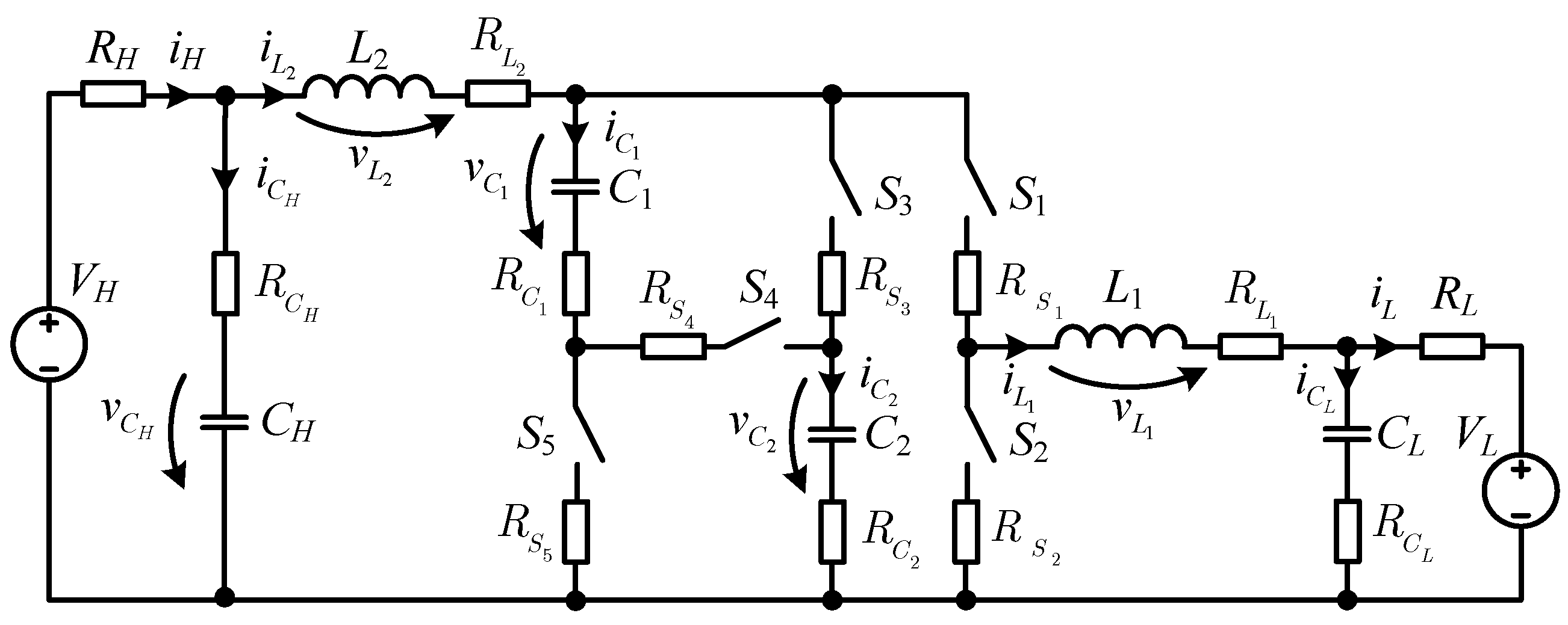
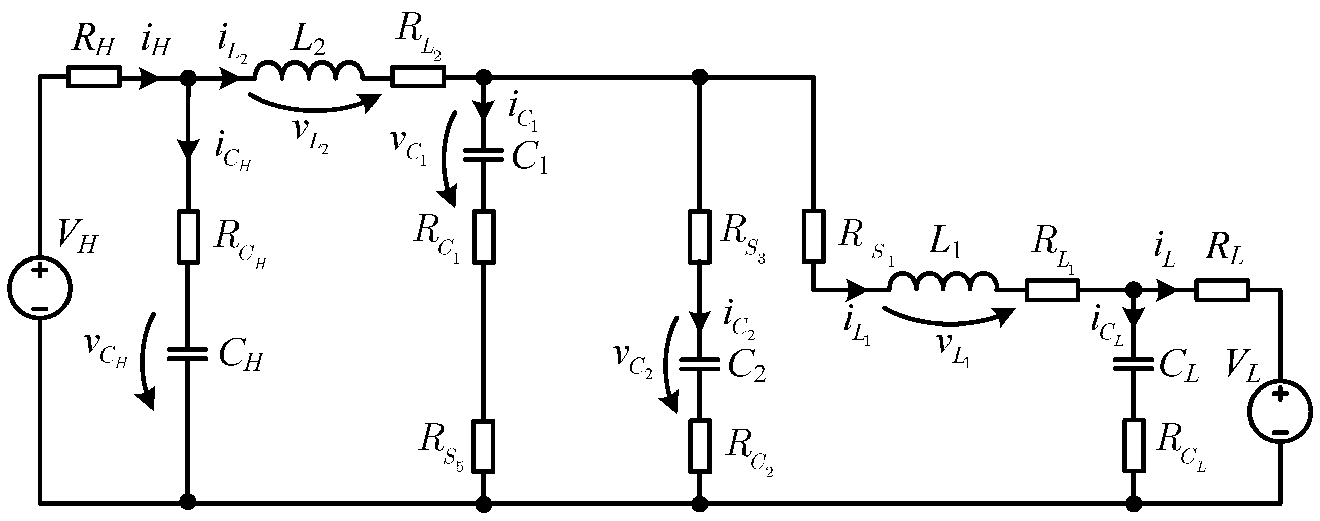
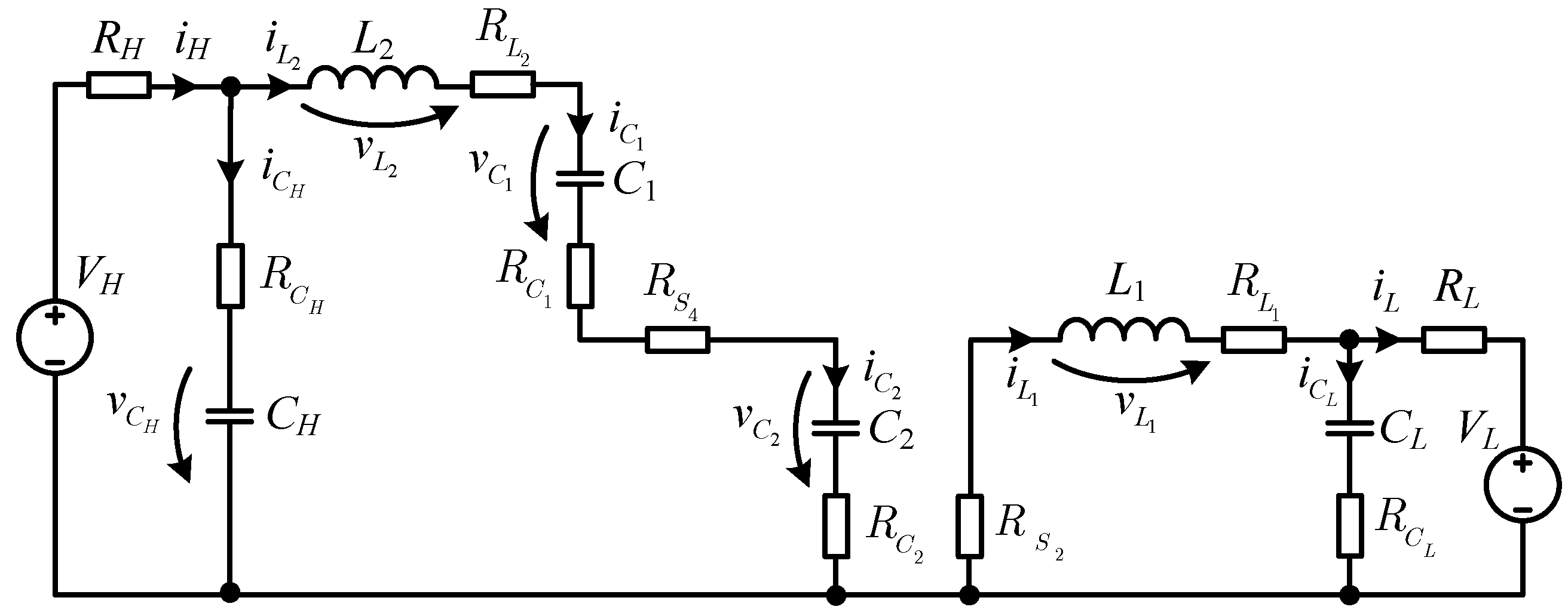
2. Hybrid Converter Topology and Theory of Operation
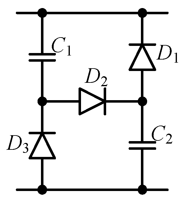
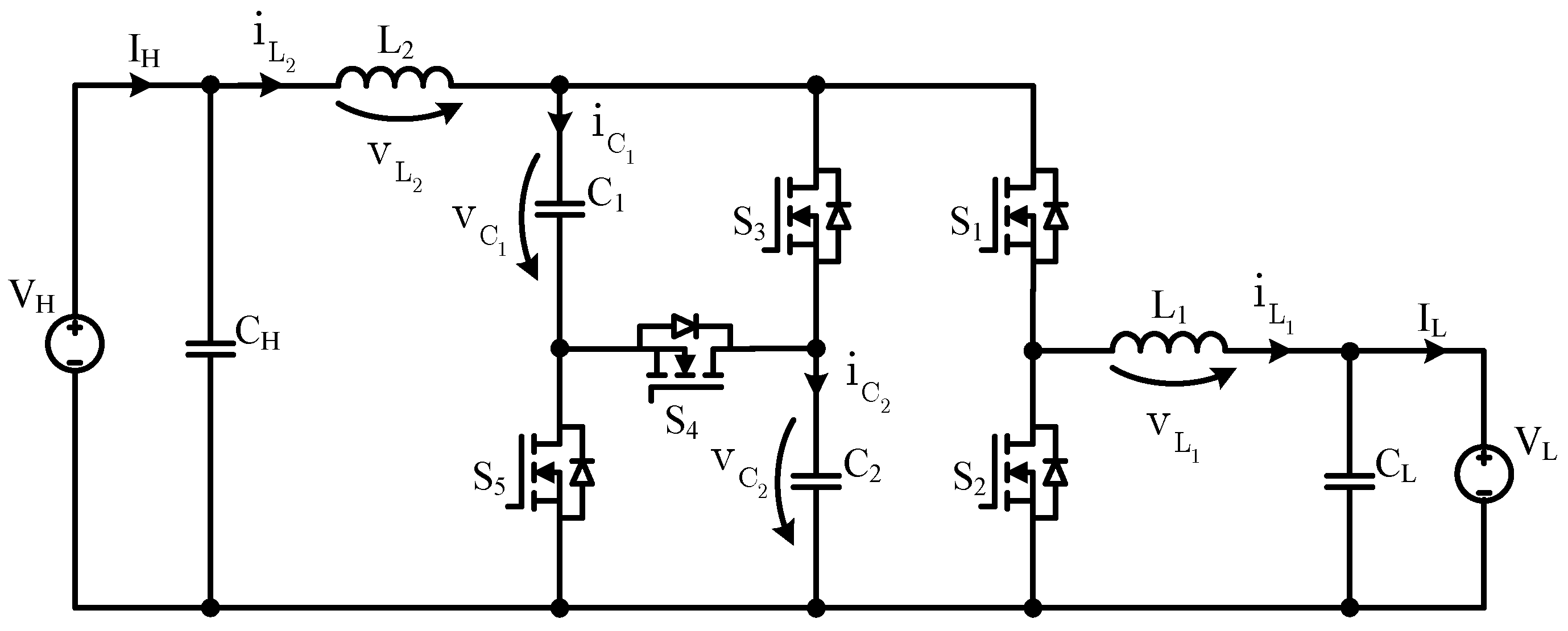
2.1. BHSC Topology

Hybrid converters are obtained from the conventional DC–DC converters by inserting switched-capacitor or switched-inductor cells in their structure [23]. Compared to the initial converter, a DC–DC hybrid converter has a higher voltage conversion ratio at the same duty cycle, being appropriate for applications where conventional DC–DC converters are operating with degraded performances due to very low or very high duty cycle values.
The step-down switched-capacitor cell described in [31] consists of two capacitors and three diodes—C1, C2, D1, D2, and D3—connected as shown in Figure 1.
A comparative evaluation of unidirectional step-down and hybrid switched-capacitor step-down DC–DC converters was presented in [32,33], based on comprehensive theoretical analysis and extensive experimental testing. This article investigates the characteristics, operation, and performance of the bidirectional hybrid switched-capacitor converter (BHSC), derived from the unidirectional hybrid step-down topology by replacing all diodes with transistors. Limited preliminary results were presented in [4].
The BHSC, presented in Figure 2, can be seen as a modified bidirectional step-down (buck) converter, with a bidirectional switched-capacitor cell inserted at the high-voltage side. Compared with other high voltage conversion ratio converters, such as those described in [33,34], the BHSC has a common ground—a direct galvanic connection between the input and output ports—which is an advantageous feature in many applications. In terms of the number of components, compared with other topologies [30,35] with the same conversion ratio, the BHSC has an additional transistor, but it provides the advantage of smaller passive components, as shown in the following sections.

2.2. BHSC Theory of Operation

The BHSC converter operates as a buck converter if it is supplied at the high-voltage (VH) side, or as a boost converter the energy is taken from the low-voltage (VL) side. The switched-capacitor cell is connected through L2 at the converter input if the BHSC operates as a step-down converter, or at the converter output if it operates as a step-up converter (in the other direction). The BHSC’s step-down operating mode is described in this article. The step-up operating mode is similar—the only difference between the two modes being the sign of the currents.
To explain the operation in the step-down operating mode, it is convenient to define the duty factor D for the steady state in relation to S1 (that is, in the position of the switch in the conventional buck converter). This also facilitates the comparison with the buck converter. Therefore, the duty cycle is as follows:
D = t o n , S 1 T = t o n f ,
where ton,S1—the time interval when S1 is in conduction—is shortened, for convenience, to ton.
Even if there are five transistors in the BHSC’s structure, there are only two converter states in one switching period T, due to the fact that only one driving signal is used, which is applied directly to S1, S3, and S5 and inverted to S2 and S4. The BHSC’s equivalent schematics for the two states, defined by the ton and toff time intervals, are shown in Figure 3 and Figure 4, respectively.
In step-down operating mode, during ton, the switched capacitors C1 and C2 are connected in parallel through S3 and S5. The current through L1 is positive and equal to the sum of the L2 current and the total discharging current of the switched-capacitor cell. During toff, C1 and C2 are connected in series through S4 and are charged with a current equal to the L2 current. L1 is decoupled from the switched capacitors, its positive current is decreasing, and a part of its energy is transferred at the low-voltage side.

2.3. Analytical Description

To simplify the analysis, we will consider the following assumptions to be valid:
(a)
The converter is operating in steady-state, continuous conduction mode (CCM);
(b)
All components are ideal;
(c)
The capacitances are large enough to achieve negligible voltage ripple; therefore, the voltage across each capacitor is considered constant;
(d)
The capacitors that form the switched-capacitor cell are considered identical (C1 = C2 = Csw).
In general, the equations for the voltages across the inductors L1 and L2, and for the currents through the switched capacitors C1 and C2 in the two states, are as follows:
t o n : v L 1 = V C 1 V L v L 2 = V H V C 2 i C 1 + i C 2 = i L 2 i L 1 t o f f : v L 1 = V L v L 2 = V H V C 2 V C 1 i C 1 = i C 2 = i L 2
Taking into consideration that the two switching capacitors are identical, Equations (2) can be simplified as follows:
t o n : v L 1 = V C V L v L 2 = V H V C 2 i C s w = i L 2 i L 1 t o f f : v L 1 = V L v L 2 = V H 2 V C i C s w = i L 2
The voltage-second balance equations for L1 and L2 are
V L 1 = D ( V C V L ) + ( 1 D ) ( V L ) = 0 V L 2 = D ( V H V C ) + ( 1 D ) ( V H 2 V C ) = 0
Equation (4) shows that the voltage across a switched capacitor can be written in two forms:
V C s w = V H 2 D V C s w = V L D
The relationship between VH and VL (i.e., the voltage conversion ratio, M), along with the duty cycle equation—both obtained from Equation (5)—are given as follows:
M = V L V H = D 2 D
D = 2 V L V H + V L = 2 M 1 + M
Equation (6) shows that the term (2-D) at the denominator yields up to twofold reduction in the voltage conversion ratio of the hybrid converter compared with a classical buck converter that operates at the same duty cycle—an important advantage for the hybrid topology.
From Equation (5), the following form of the capacitor voltage can be obtained, showing that in steady-state operation it is only dependent on the two input voltages:
V C = V H + V L 2
The key theoretical waveforms of the BHSC for the steady-state, step-down operating mode are presented in Figure 5. The relationships between the inductor currents iL1 and iL2, the inductor voltages VL1 and VL2, and the switched capacitor currents in the two switching states are in evident concordance with the above explanations and equations. The input and output voltage ripples (ΔVCH, ΔVCL) are represented considering ideal capacitors and constant current at the two ports.

3. Sizing of BHSC Components

An important aspect of any converter design, with impact on the stability, is the sizing of its components, which is addressed in this section.

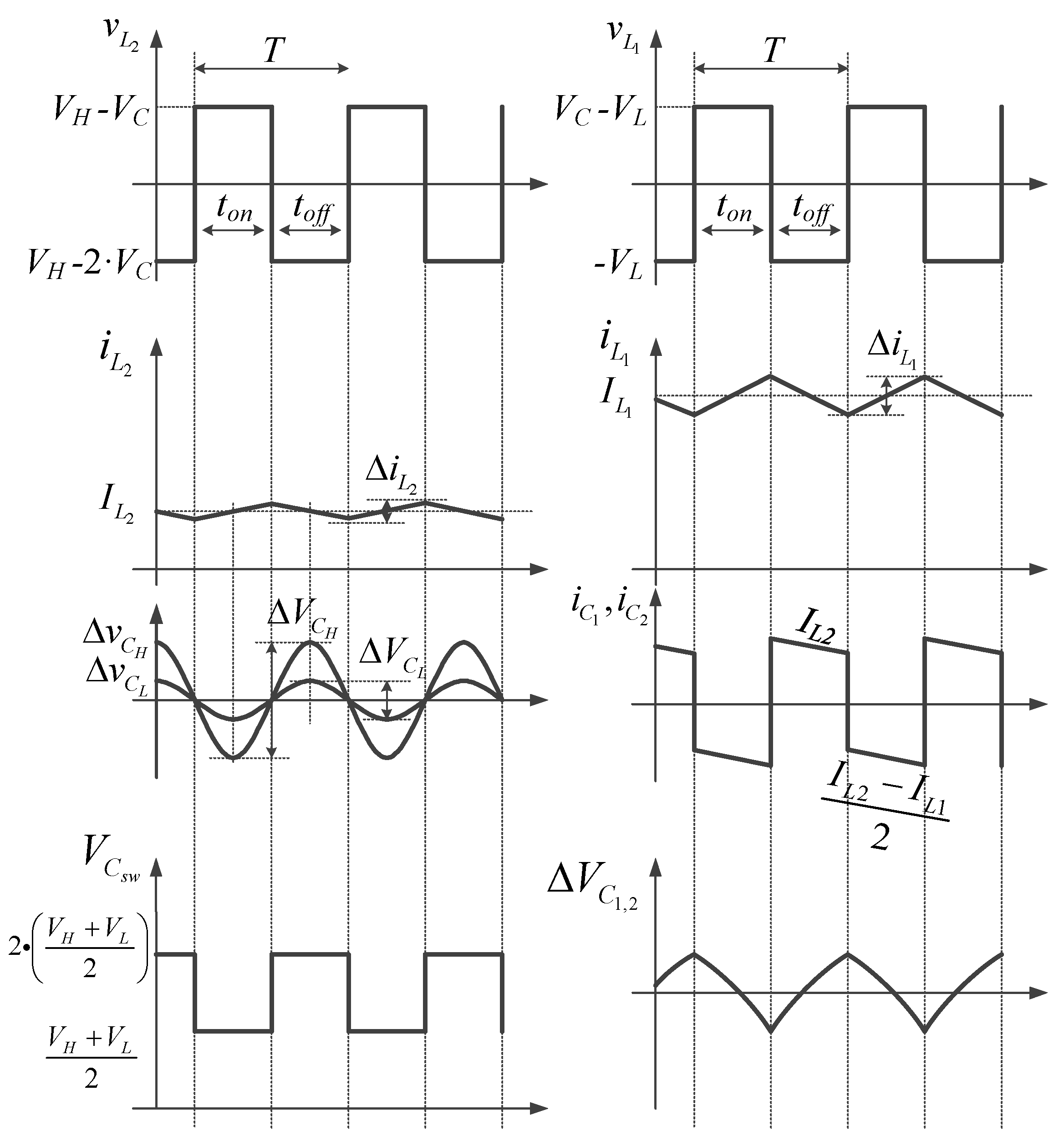
3.1. Inductor Sizing

Starting from Equation (3), the inductance value of each inductor can be calculated using the value of the ton time interval and a chosen value for the inductor current ripple. Therefore, with the assumption of linear inductor current variation, Equation (3) can be rewritten as follows:
t o n : L 1 d i L 1 d t = V C s w V L L 1 Δ i L 1 t o n = V C s w V L L 2 d i L 2 d t = V H V C s w L 2 Δ i L 2 t o n = V H V C s w
The inductance values from Equation (9) can be rewritten as follows:
L 1 = D T ( V C s w V L ) Δ i L 1 L 2 = D T ( V H V C s w ) Δ i L 2
To compare the BHSC topology with other similar converters, the passive components were calculated allowing for a percentage current ripple (ri [%])—the same for each of the compared converters. The real values of the inductor current ripples are
Δ i L 1 = r i I L 1 Δ i L 2 = r i I L 2
Using Equations (5), (6), (10), and (11), the following equations for the calculation of inductance values were obtained:
L 1 = V L ( V H V L ) r i f I L 1 ( V H + V L ) L 2 = V H ( V H V L ) r i f I L 2 ( V H + V L )
These equations show that the inductance values depend only on the operating point (through VL, VH, and the average input and output currents IL1 and IL2) and on the chosen value for ri.

3.2. Capacitor Sizing

Capacitor sizing was performed in a similar way, starting from the equations that show the dependency between the capacitor currents (expressed using the capacitances and the voltage derivatives) and the inductor currents.
C s w d v C s w d t = i L 2 i L 1 2 C L d v C L d t = i L 1 I L 1 C H d v C H d t = i L 2 I L 2 ,
Equation (13) can be rewritten as follows:
C s w = 1 2 Δ v C s w 0 t o n ( i L 2 i L 1 ) d t C L = 1 Δ v C L t o n / 2 t o n + t o f f / 2 ( i L 1 I L 1 ) d t C H = 1 Δ v C H t o n / 2 t o n + t o f f / 2 ( i L 2 I L 2 ) d t
A percentage voltage ripple was allowed for the voltages across the capacitors. The real values of the capacitor voltage ripples can be calculated using the imposed percentage voltage ripple (rv[%]):
Δ v C = r v V C s w Δ v C L = r v V C L Δ v C H = r v V C H
The final form of the capacitance values, given in Equation (16), was obtained taking into account Equations (14) and (15), along with the waveforms from Figure 5.
C s w = 2 I L V L ( V H V L ) r v f V H ( V H + V L ) 2 C L = r i I L 8 r v f V L C H = r i I L V L 8 r v f V H 2
An important aspect related to the capacitance values derived from Equation (16) is that, under certain conditions, when using capacitors with these values, instabilities may occur during the operation of the converters. If necessary, adjustments of these values can be carried out to ensure the system’s stability. However, the values given by Equation (16) were used for comparison with other topologies, as the adjustments for each of the compared converters are difficult to take into account.

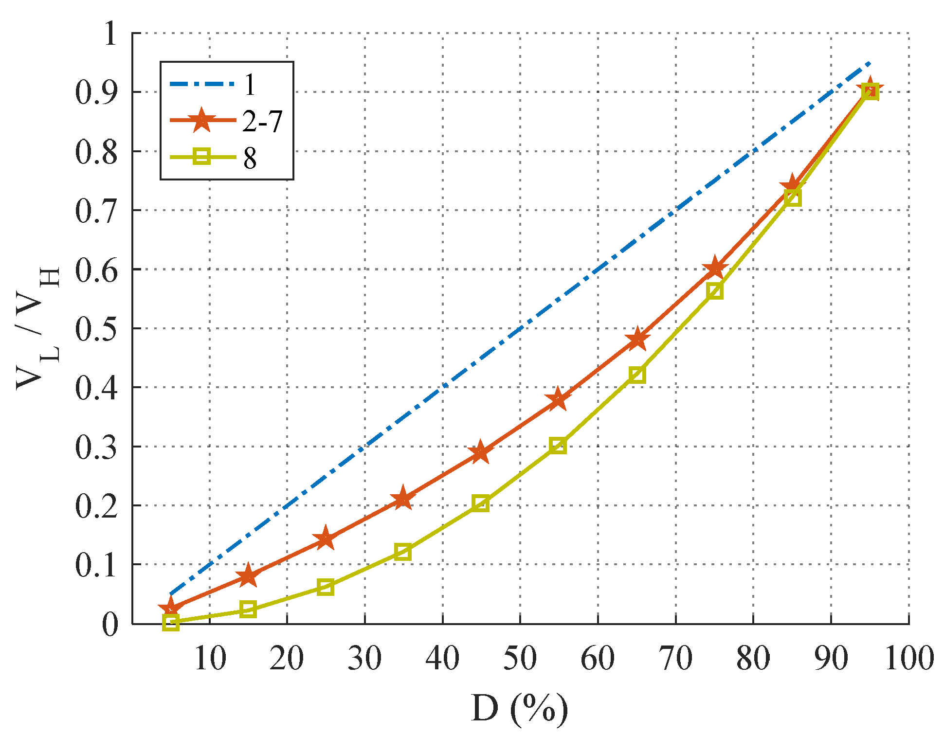
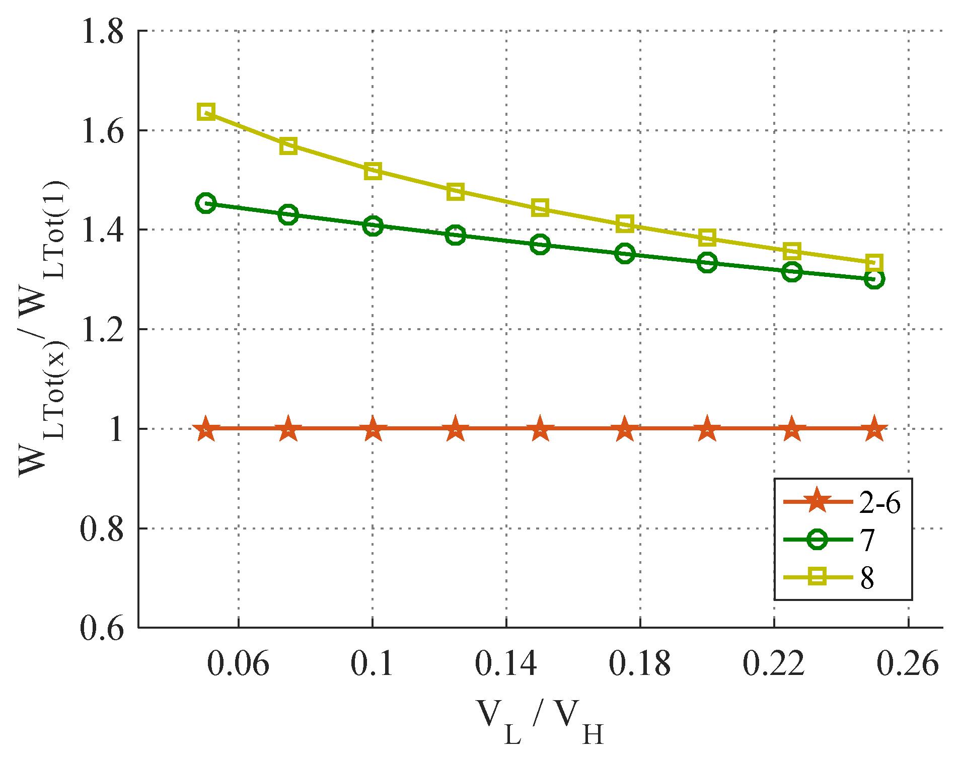
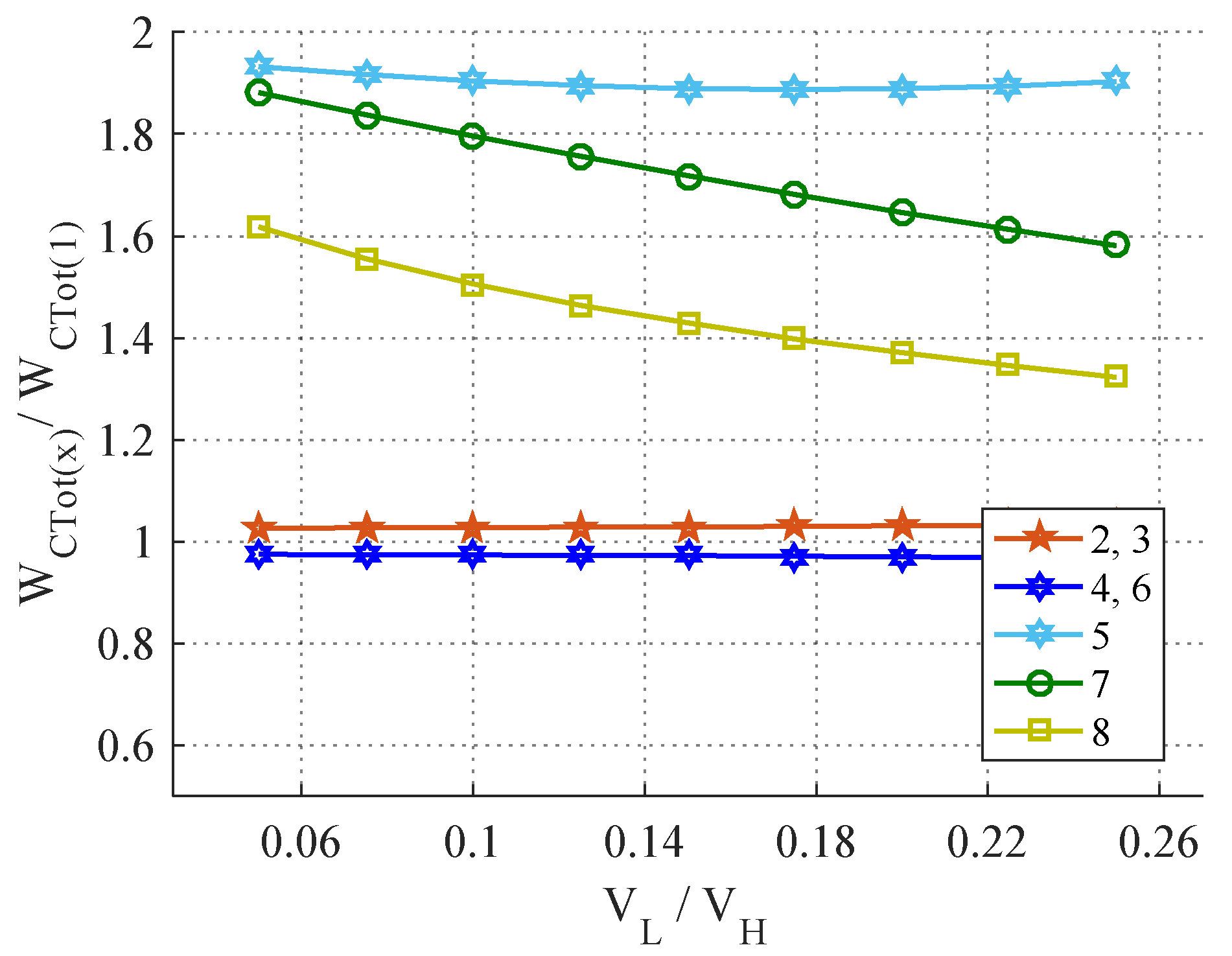
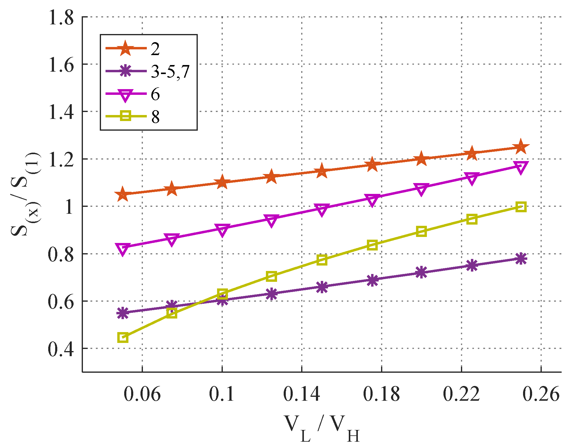
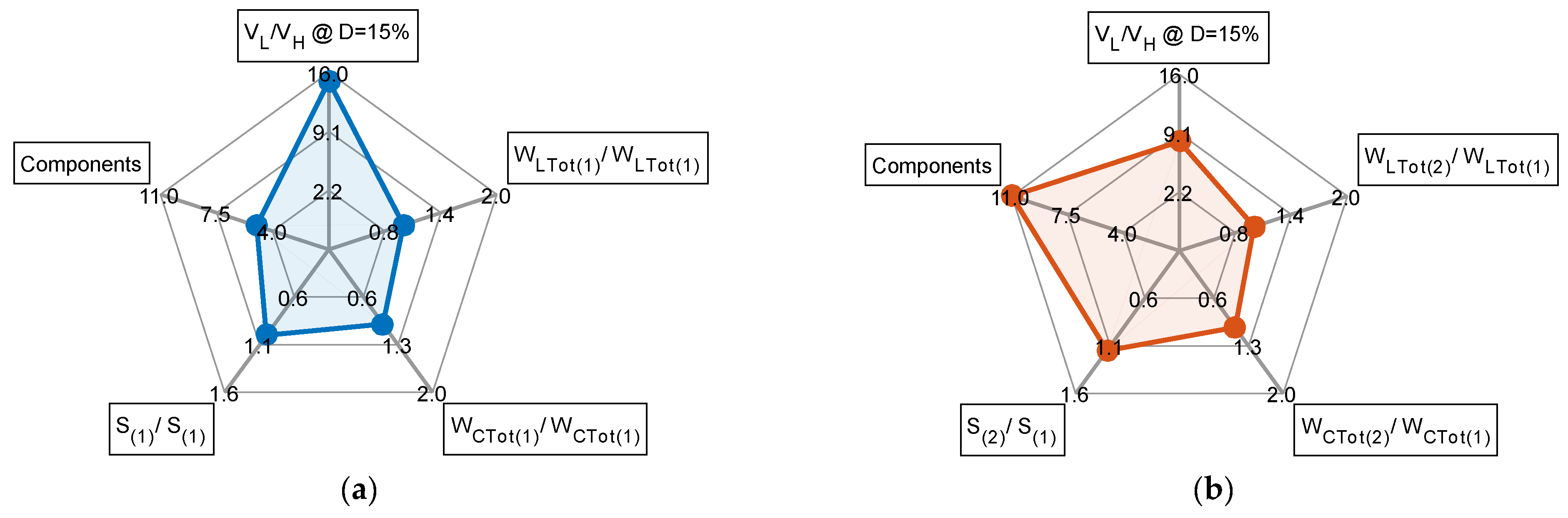
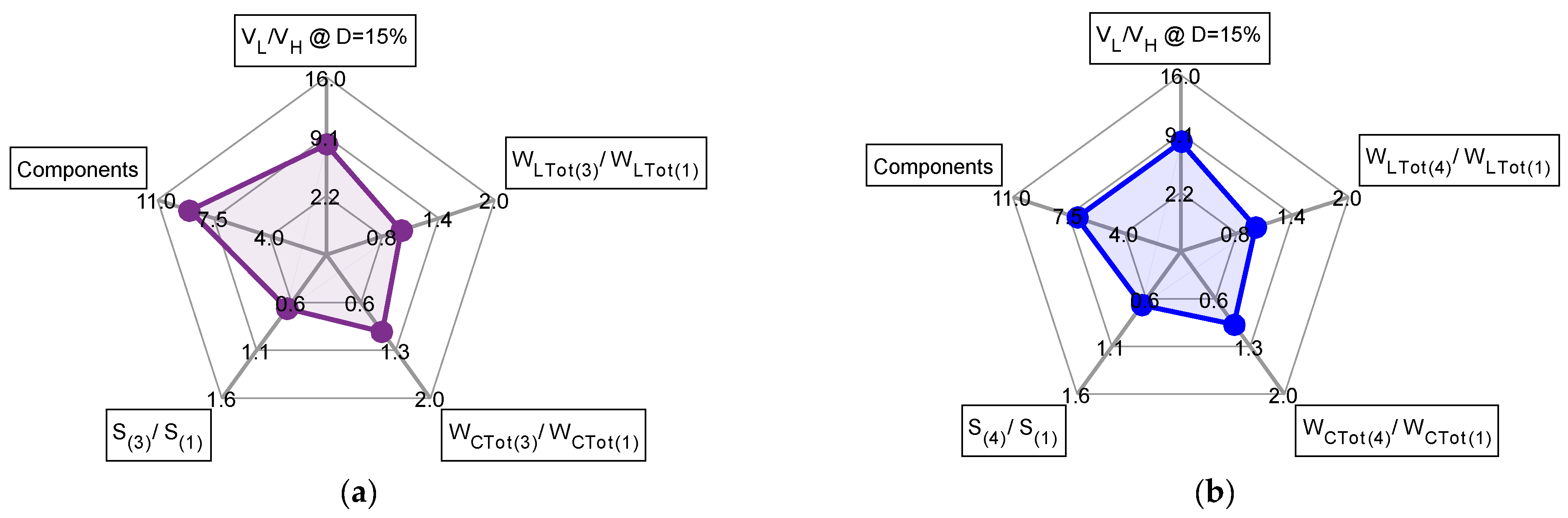
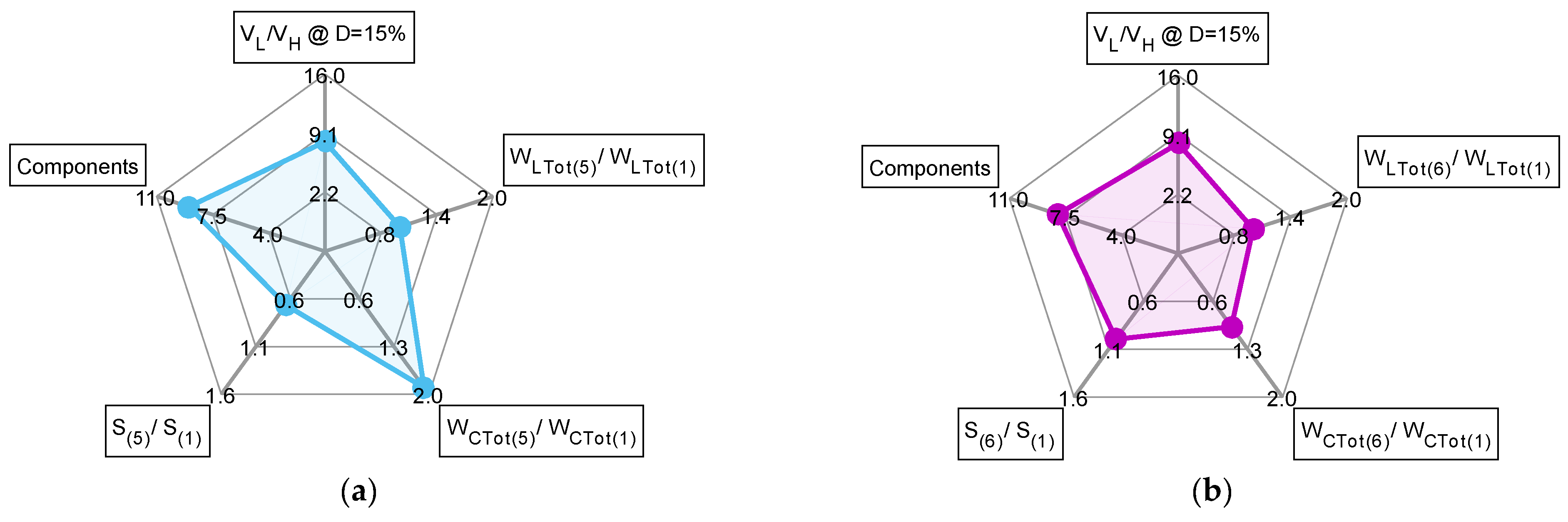
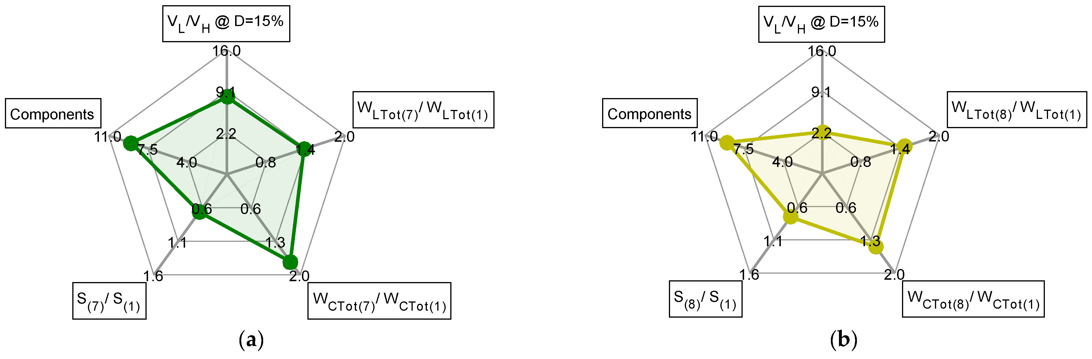
4. Comparison with Other Converters

To compare the BHSC with other similar converters, the total energy of the inductors, the total energy of the capacitors, and the total switch stress were used as metrics. The total energy of the passive components is roughly proportional to the cost and the volume of a DC–DC converter. On the other hand, the total switch stress of a converter is related to the cost of the switches and the switch losses; therefore, it shows the impact of the switches on the total cost and on the converter’s efficiency.
The energy of each inductor is calculated as shown in Equation (17). The total energy of the converter inductors is given in Equation (18).
W L 1 = L 1 I L 1 2 2 = I L V L ( V H 2 V L 2 ) r i f ( V H + V L ) W L 2 = L 2 I L 2 2 2 = I L V L 2 ( V H V L ) 2 r i f V H ( V H + V L )
W L T o t = W L 1 + W L 2 = I L V L ( V H V L ) 2 r i f V H
The energy stored in each capacitor is calculated using Equation (19), with the final expression as shown in Equation (20). The capacitors connected at the two ports (CH and CL) have equal stored energy, due to having the same parameter values and sizing equations.
W C s w = C s w V C s w 2 2 W C L = C L V L 2 2 W C H = C H V H 2 2
W C s w = I L V L ( V H V L ) 4 r v f V H W C L = W C H = r i I L V L 16 r v f
The total energy of the converter capacitors is given in Equation (21). Using Equation (20), it can be written as shown in Equation (22).
W C T o t = 2 W C s w + W C L + W C H
W C T o t = I L V L ( V H ( 4 + r i ) 4 V L ) 4 r v f V H
The total switch stress of the converter is obtained by summing the products between the maximum voltage and maximum current of each switching device, as shown in Equation (23).
S T o t a l = j = 1 5 V S j I S j
The maximum values for the voltage and the current of each switching device are given in Equation (24).
V S 1 = V H + V L V S 2 = V S 3 = V S 4 = V H + V L 2 I S 1 = I S 2 = I L I S 3 = I S 5 = I H I L 2 I S 4 = I H
Using Equation (24), a simple expression is obtained for the total switch stress of the converter:
S T o t a l = 2 I L V H + V L
We used Equations (18), (22), and (25) to compare the BHSC with other topologies. The voltage conversion ratios are shown in Figure 6. The values of each compared converter were divided by the corresponding values of the conventional buck converter, and they are graphically represented in Figure 7, Figure 8 and Figure 9.
The voltages selected for comparison were VH = 400 V and VL = 20 V…100 V, in order to achieve a conversion ratio (VL/VH) between 5% and 25%. A common value for the inductor current ripple percentage was chosen, i.e., ri = 20%, or other optimal values can be used. Other topologies were selected for comparison, most with the same voltage conversion ratio together with a quadratic converter; their characteristics are presented in Table 1. From these results, it can be noticed that the BHSC converter achieves a conversion ratio between that of the conventional buck–boost converter (1) and the quadratic converter (8). In order to achieve this conversion ratio, the BHSC requires the same inductive and capacitive energies as the conventional converter, but lower compared with other topologies. The cost of achieving a common ground between inputs is seen in the total stress on the active switches, which is slightly higher compared with the selected topologies. The main characteristics of the selected converters are also presented in Figure 10, Figure 11, Figure 12 and Figure 13 in a more concise representation. The voltage conversion ratio VL/VH is multiplied with 100 in these figures.

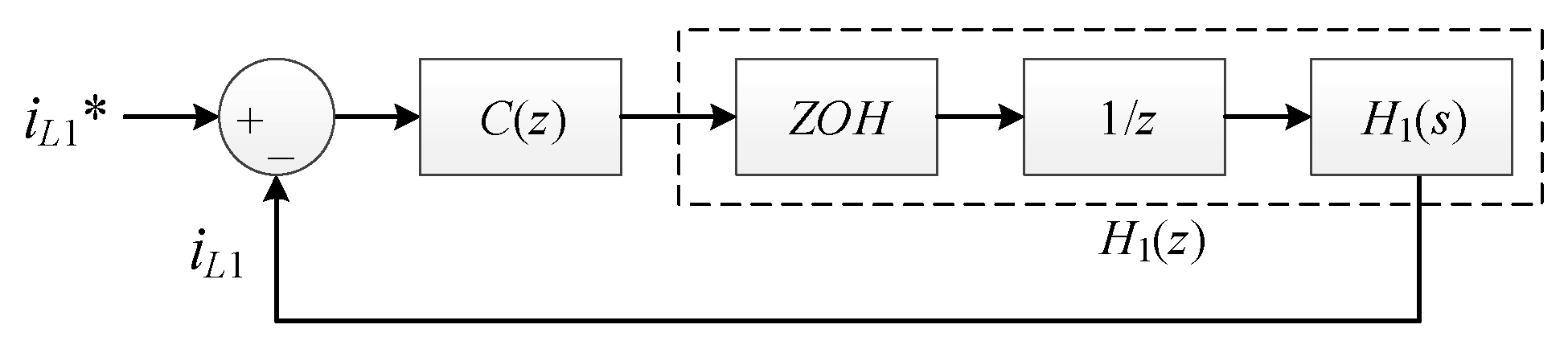
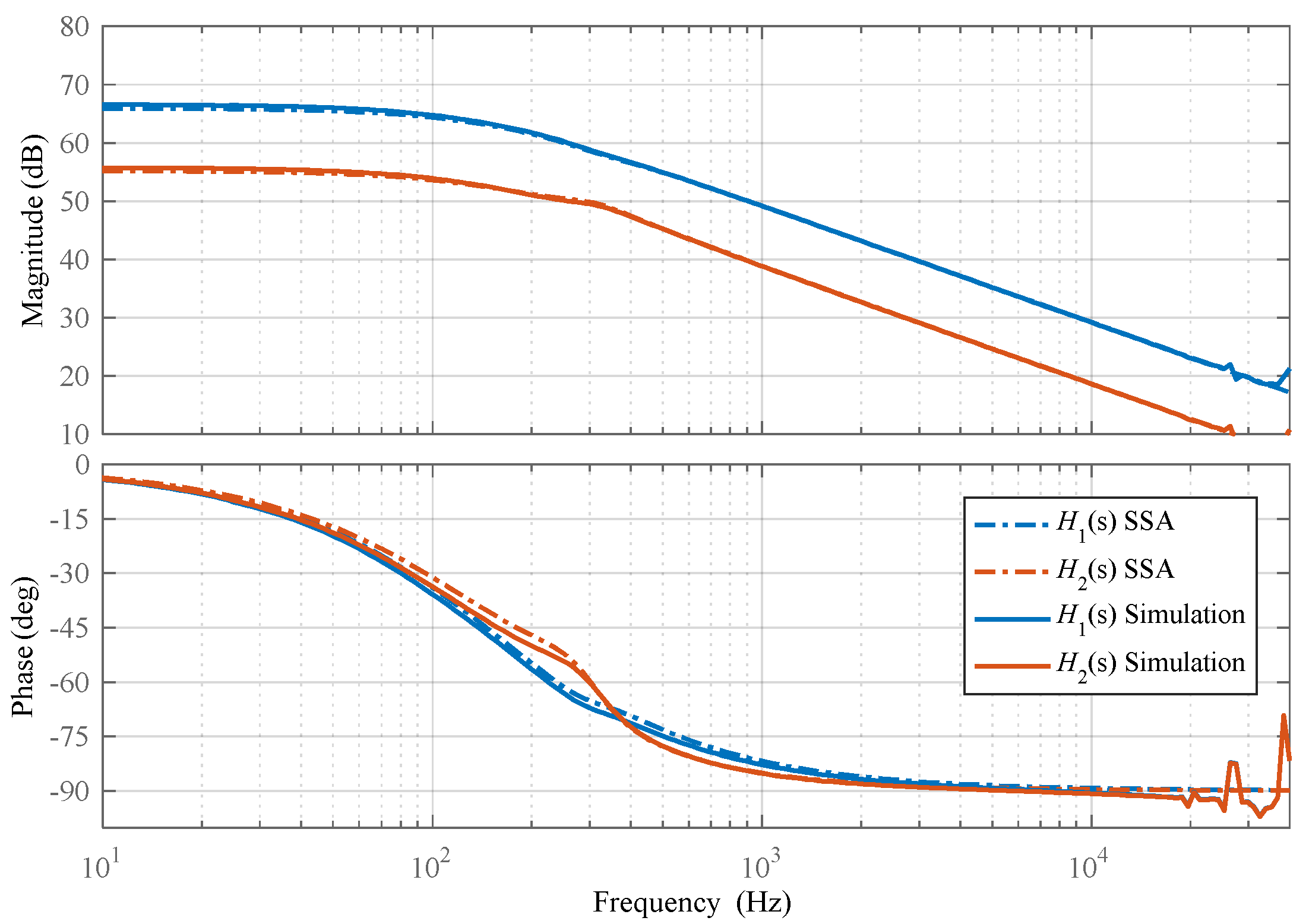
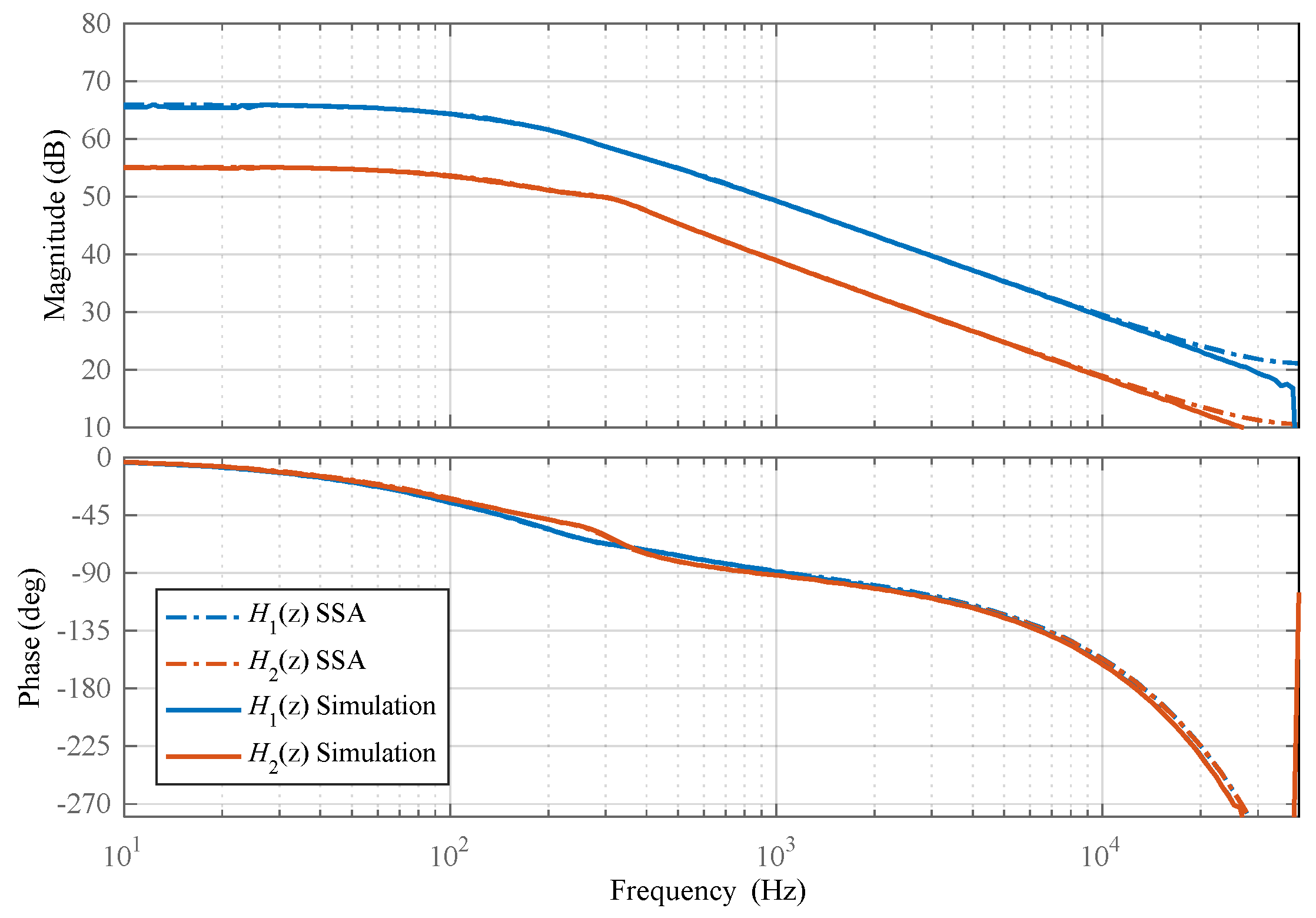
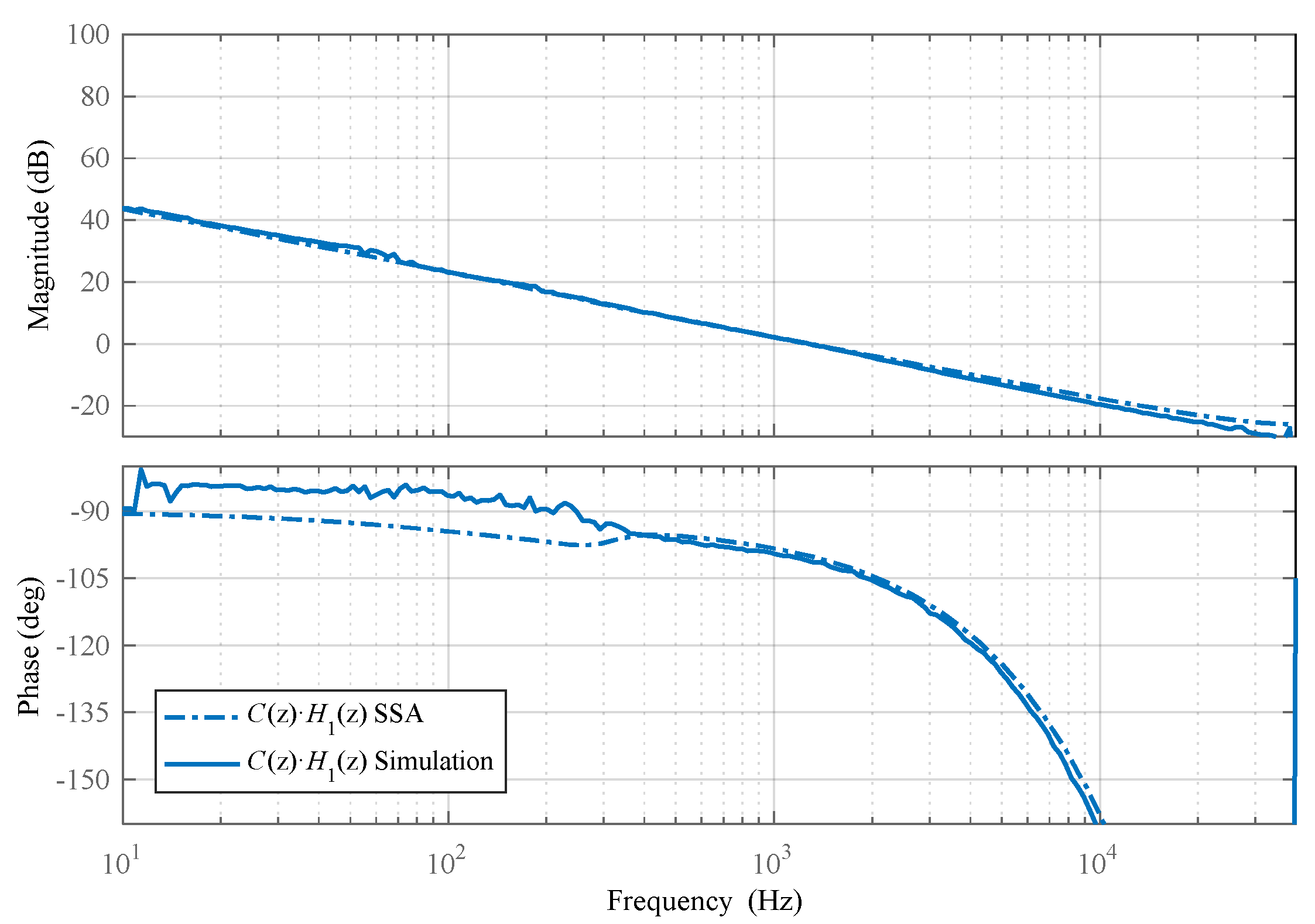
5. Stability Analysis

In this section, the BHSC’s stability is investigated using the state-space averaging (SSA) method, in order to obtain the necessary information for current controller design, which guarantees the converter’s operation without undamped oscillations or instability phenomena.
The following hypotheses are considered valid for stability analysis:
(a)
The power switching devices S1–S5 are ideal switches in series with parasitic resistances rS1 = … = rS5 = rS;
(b)
VL and VH have constant values during one switching period T;
(c)
L1 and L2 have the parasitic series resistances rL1 and rL2, respectively;
(d)
C1 and C2 have equal parasitic series resistances; rC1 = rC2 = rc;
(e)
CL and CH have the parasitic series resistances rCL and rCH, respectively.
To assess stability, SSA first assembles a continuous-time averaged model of the converter, which contains the contributions of all operating states that are contained within a switching period.
All of the parasitic resistances of the active passive components have to be introduced in the BHSC schematic, in order to correctly assess the converter and the system stability. Due to the relatively high number of passive components, the converter could behave like a high-order system, with possible well-known stability problems for such systems. However, it has been shown in other articles [36] that under some circumstances the effects of inductors and capacitors cancel one another out, resulting in lower-order system behavior. It is the responsibility of the designer to decide on the values of the parasitic components so as to reduce the order of the equivalent average model of the converter. Figure 14 presents the converter schematics, prepared for stability analysis, and the equivalent BHSC circuits for ton and toff are presented in Figure 15 and Figure 16, respectively.
The input and input vector are defined as follows:
x T = i L 1 i L 2 v C s w v C L v C H , u = V L V H .
The state-space representation for ton and the corresponding matrices are given in Equations (27)–(29).
x ˙ = A 1 x + B 1 u
A 1 = R C s w 2 + R L 1 + R S 1 + R S 3 2 + R C L · R L R C L + R L L 1 R C s w 2 + R S 3 2 L 1 1 L 1 R C L R C L + R L 1 L 1 0 R C s w 2 + R S 3 2 L 2 R C s w 2 + R L 2 + R S 3 2 + R C H · R H R C H + R H L 2 1 L 2 0 R C H R C H + R H 1 L 2 1 2 · C s w 1 2 · C s w 0 0 0 R L C L · ( R C L + R L ) 0 0 1 C L · ( R C L + R L 0 0 R H C H · ( R C H + R H ) 0 0 1 C H · ( R C H + R H )
B 1 = R C L L 1 ( R C L + R L 0 0 R C H L 2 ( R C H + R H ) 0 0 1 C L ( R C L + R L ) 0 0 1 C H ( R C H + R H )
The state-space representation for toff and the corresponding matrices are given in Equations (30)–(32).
x ˙ = A 2 x + B 2 u
A 2 = R L 1 + R S 2 + R C L · R L R C L + R L L 1 0 0 R C L R C L + R L 1 L 1 0 0 2 · R C s w + R L 2 + R S 4 + R C H · R H R C H + R H L 2 2 L 2 0 R C H R C H + R H 1 L 2 0 1 C s w 0 0 0 R L C L · ( R C L + R L ) 0 0 1 C L · ( R C L + R L 0 0 R H C H · ( R C H + R H ) 0 0 1 C H · ( R C H + R H )
B 2 = R C L L 1 ( R C L + R L 0 0 R C H L 2 ( R C H + R H ) 0 0 1 C L ( R C L + R L ) 0 0 1 C H ( R C H + R H )
According to SSA method, the state-space representation of the equivalent average model of the system is given as follows:
x ˙ = A x + B u ,
where the matrices A, B, and C are obtained from Ai, Bi, and Ci (i = 1; 2) through a weighted summation:
A = A 1 D + A 2 ( 1 D ) B = B 1 D + B 2 ( 1 D )
The average converter model whose state equations are described in Equations (33) and (34) is also valid if the duty cycle changes slightly around the steady-state value D. In this case, D is replaced by d = D +in Equation (34). The system in Equation (35), which represents the converter response at small signal variation, is obtained by linearization around a steady-state duty cycle D. The equivalent matrixes Ae and Be are expressed in Equation (36).
x ˜ ˙ = A e x ˜ + B e d ˜ y ˜ = C e x ˜
A e = ( A 1 D + A 2 ( 1 D ) ) B e = [ ( A 1 A 2 ) X + ( B 1 B 2 ) u ]
From Equation (35), the equation of the control variable (also a state variable of the average system) as a function of the small variation of the duty cycle is obtained:
y ˜ = C e ( s I A e ) 1 B e d ˜
Due to the bidirectional nature of the converter, any of the two inductor currents—iL1 or iL2—can be used as a control variable. It is useful to investigate both transfer functions and eventually to choose the most convenient approach for stability. The equivalent matrices for iL1 or iL2 are as follows:
C e = [ 1 0 0 0 0 ] , i L 1
C e = [ 0 1 0 0 0 ] , i L 2
The transfer functions of the inductor currents are as follows:
H 1 ( s ) = y ˜ 1 ( s ) d ˜ ( s ) = i ˜ L 1 ( s ) d ˜ ( s ) , H 2 ( s ) = y ˜ 2 ( s ) d ˜ ( s ) = i ˜ L 2 ( s ) d ˜ ( s ) ,
which were obtained from Equation (37), taking into account Equations (38) and (39), respectively.
The block diagram of the control loop is presented in Figure 17. The Bode diagrams of H1(s) and H2(s) are presented in Figure 18. The transfer functions are discretized with the ZOH method, and a supplementary time delay is added to account for both PWM and ADC delay. The discrete transfer functions H1(z) and H2(z) are presented in Figure 19. The diagrams of the transfer functions obtained through the SSA method are compared with the diagrams obtained through digital simulations carried out on a BHSC switching model, including the digital controller (TMS320F28379D) for Figure 18, resulting in unnoticeable differences between them.
The component values and the parasitic resistance values used in the calculation of the two transfer functions are given in Table 2 and they are the data catalogue values of the real components used for the BHSC prototype presented in the following section. As can be noted from Figure 18 and Figure 19, the frequency response is characteristic of a first-order system for both currents, even though the number of passive components is high. The current through iL1 was chosen as a control variable, as it has larger values than iL2. The poles and zeros of the two transfer functions are given in Table 3.
A digital current controller was designed for overall system stability (BHSC + controller), based on the H1(z) transfer function. Its transfer function is given as follows:
C ( z ) = 0.0044281 ( z 0.9865 ) z 1
The Bode diagram of the transfer function of the BHSC convertor with the controller is presented in Figure 20. The frequency response of C(z)∙H1(z) shows good stability, due to the displayed phase margin of 80 degrees at a 1.29 kHz crossover frequency.
Digital simulations were carried out to check the stability of the system under various conditions. Selected waveforms are presented in Figure 21 and Figure 22. In Figure 21, a step change in the reference current from +50 A to −50 A was applied to test the behavior of the system under large step variation. The controlled current has no overshoot, and only low oscillations are present in the current of the other current. Small oscillations are also present in the voltages across the switched capacitors. In Figure 22, a step change in the reference current from +10 A to −10 A was applied, and a similar behavior can be observed. It is important to note that the transition from one operating mode to the other is very smooth.

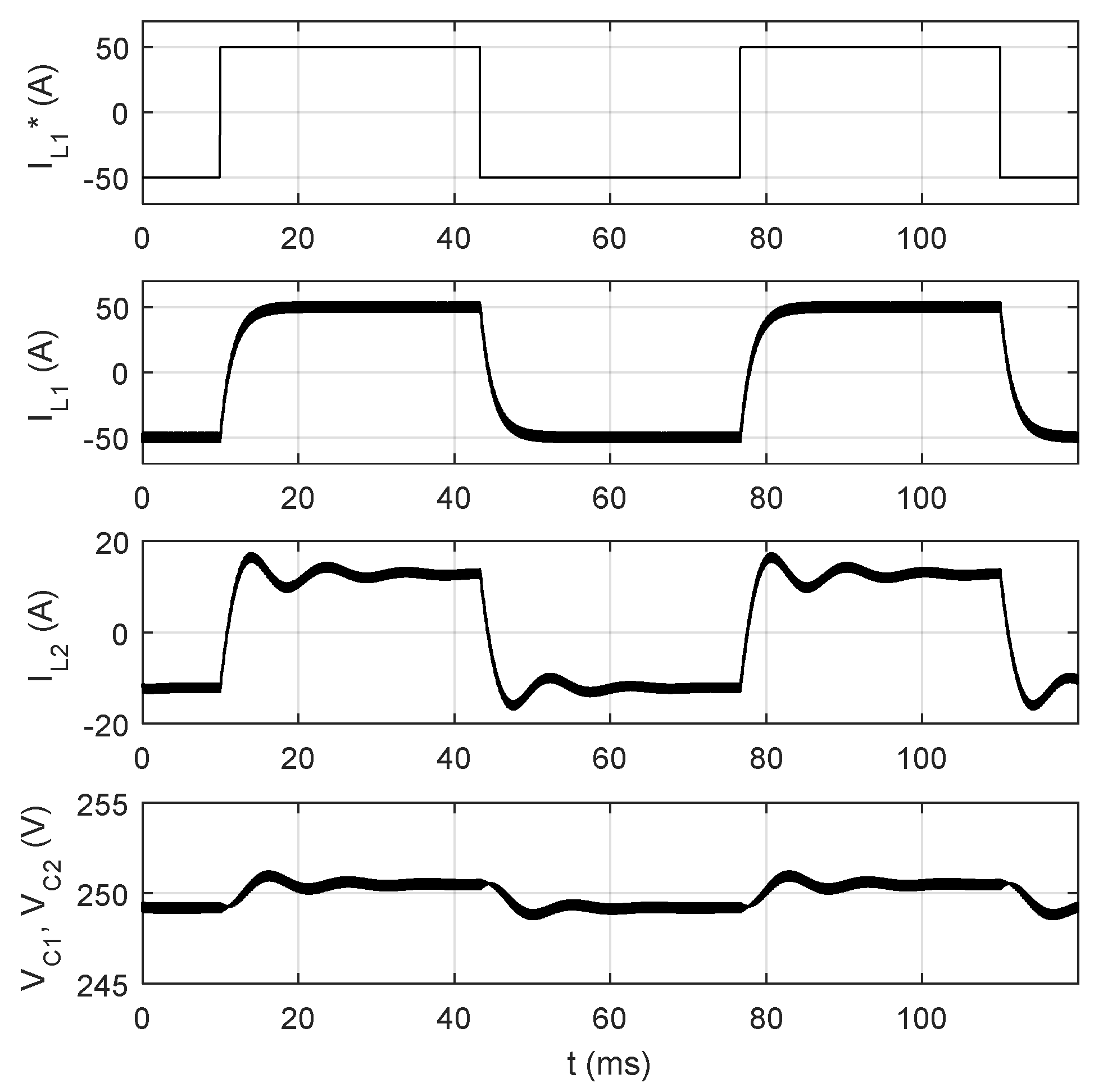
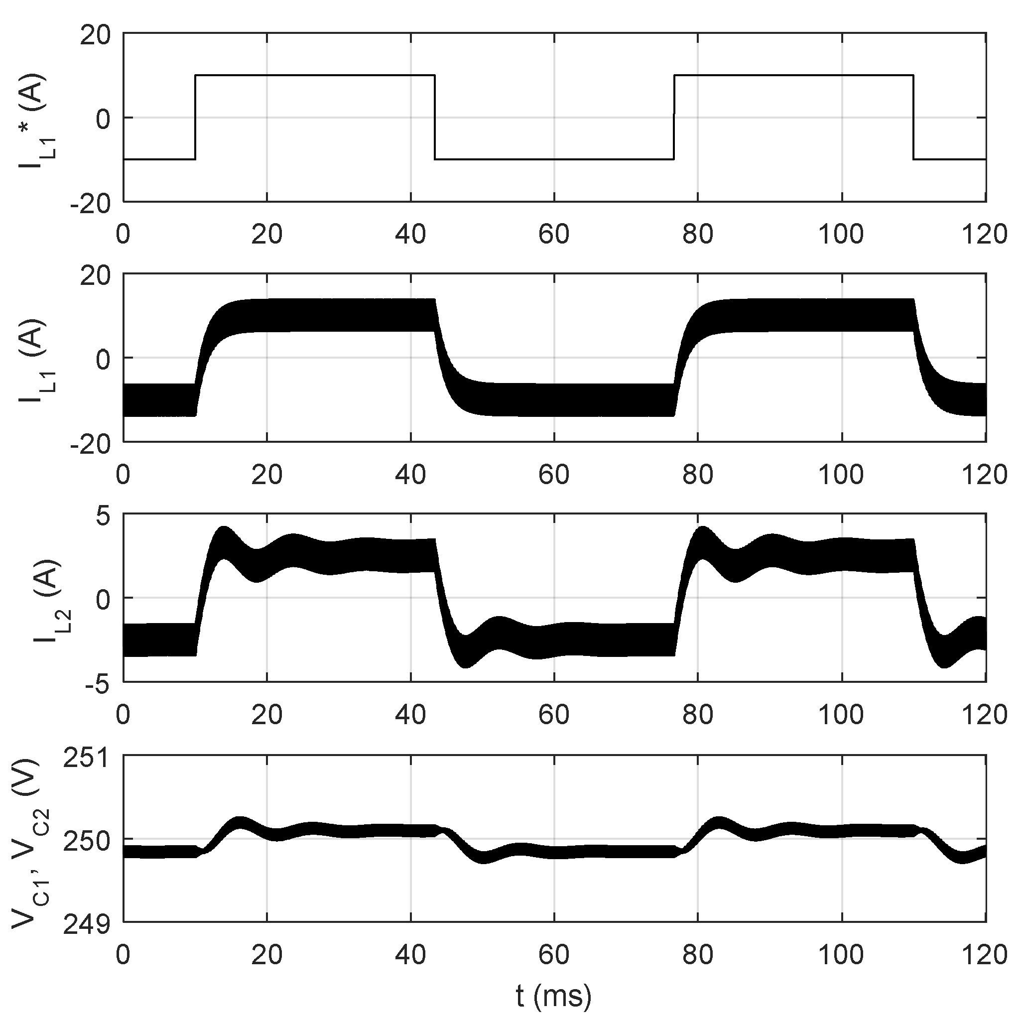
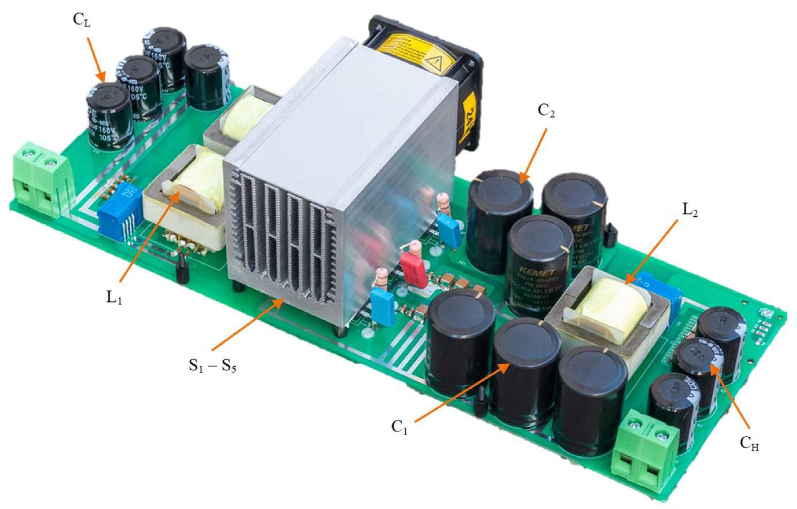
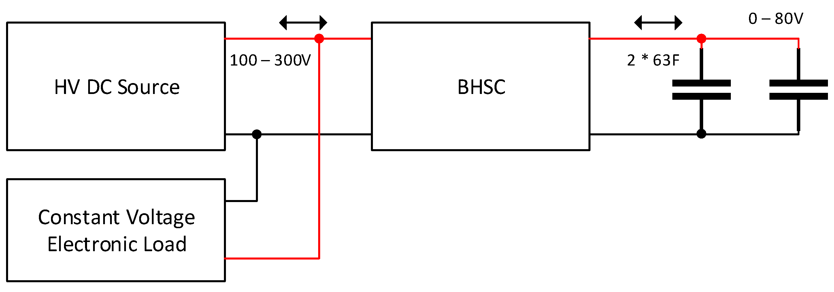
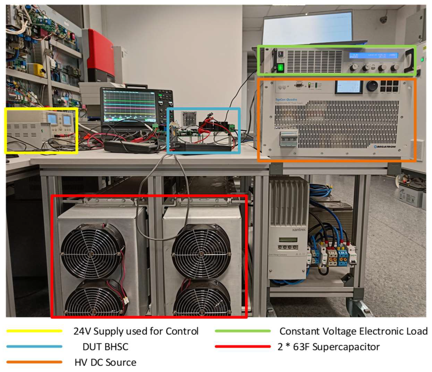
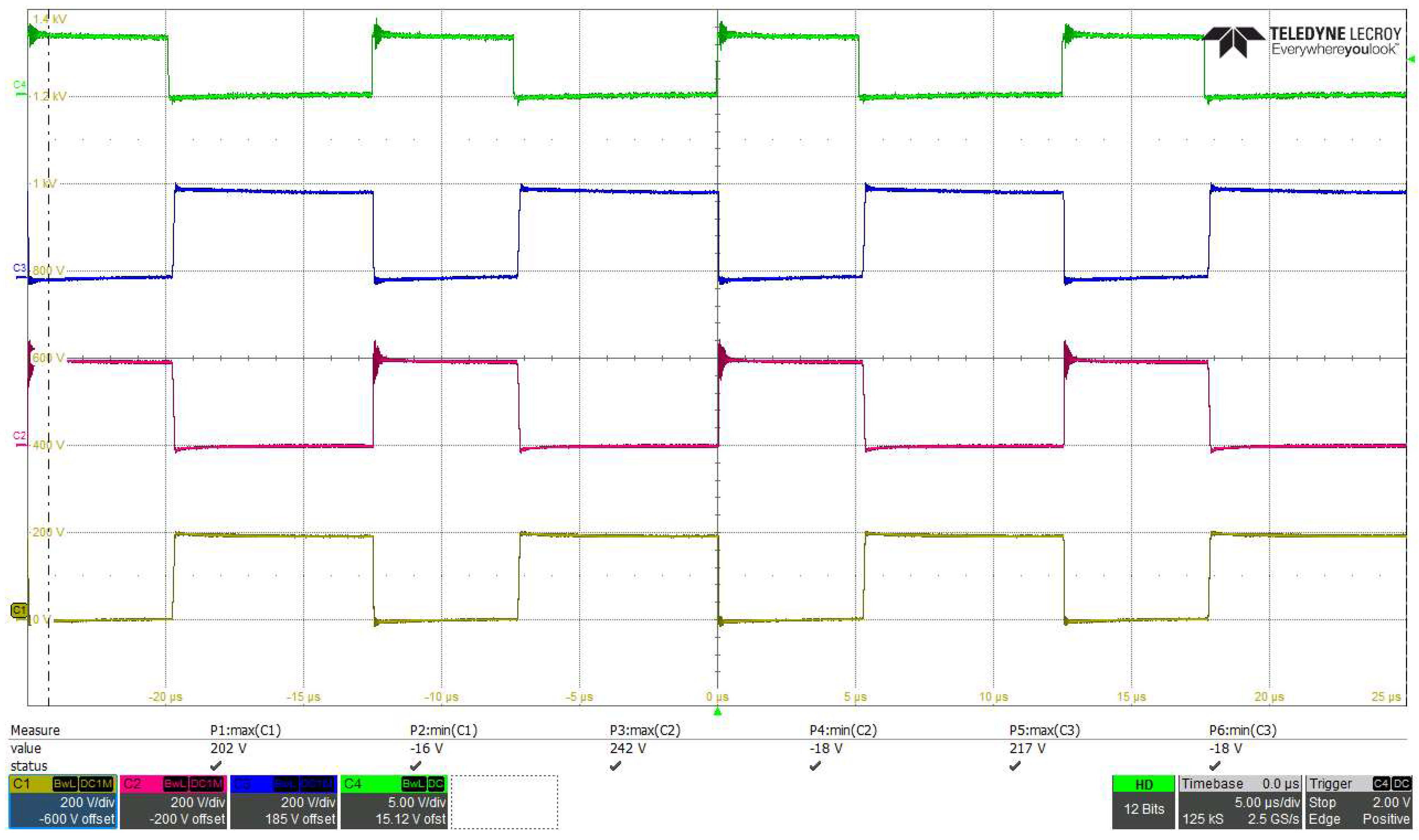
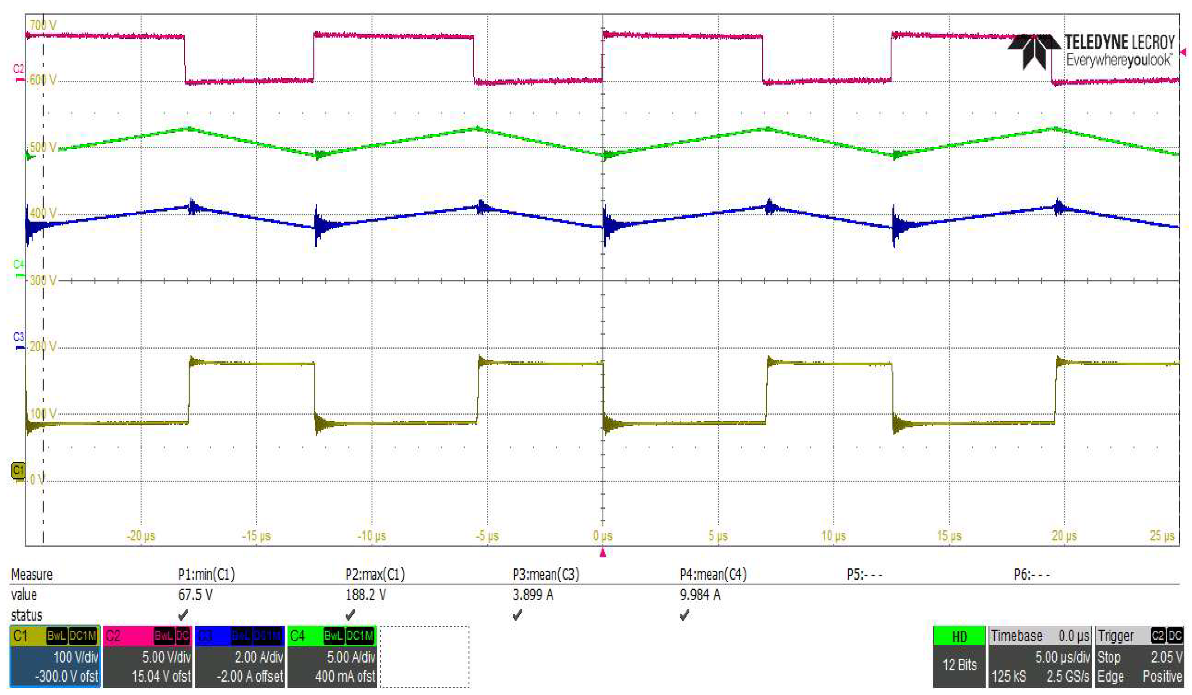
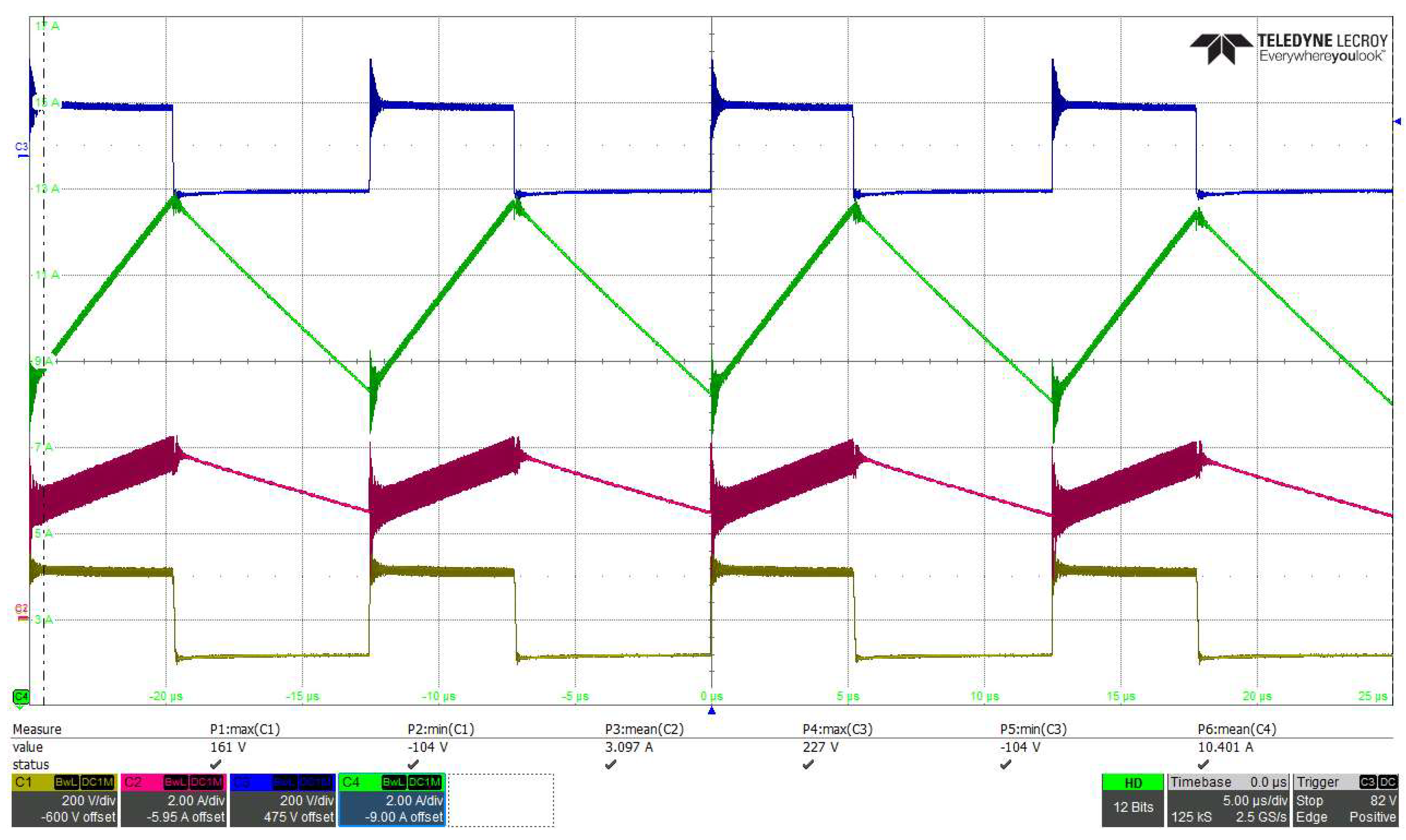
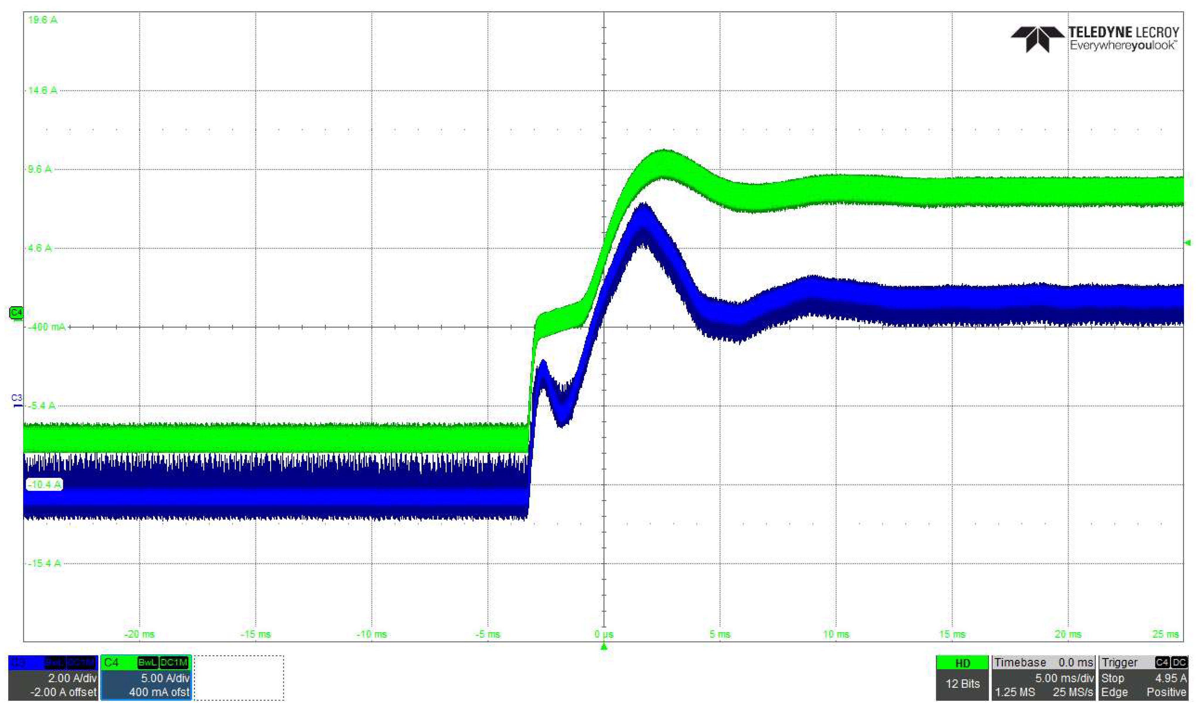
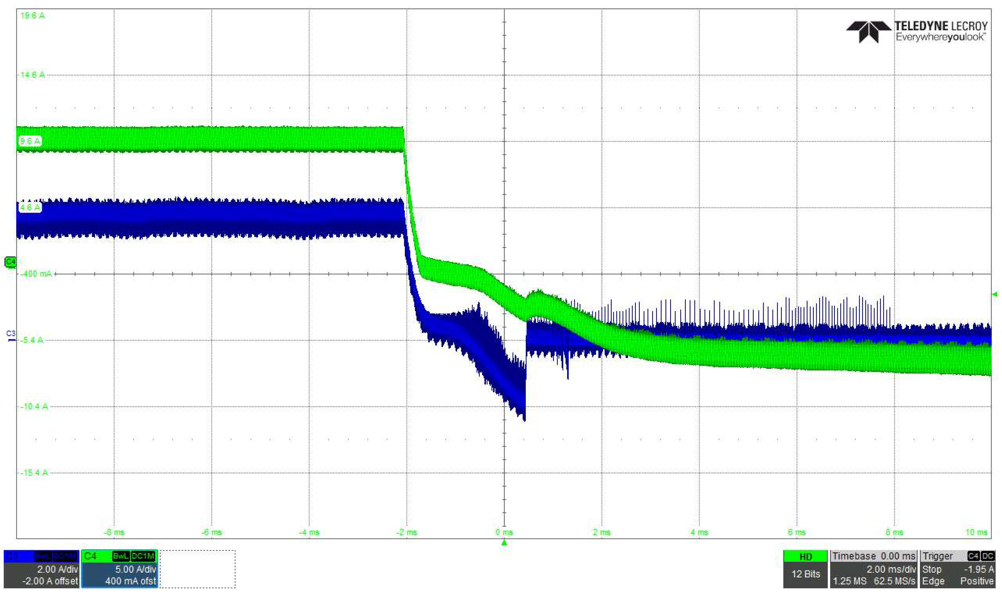
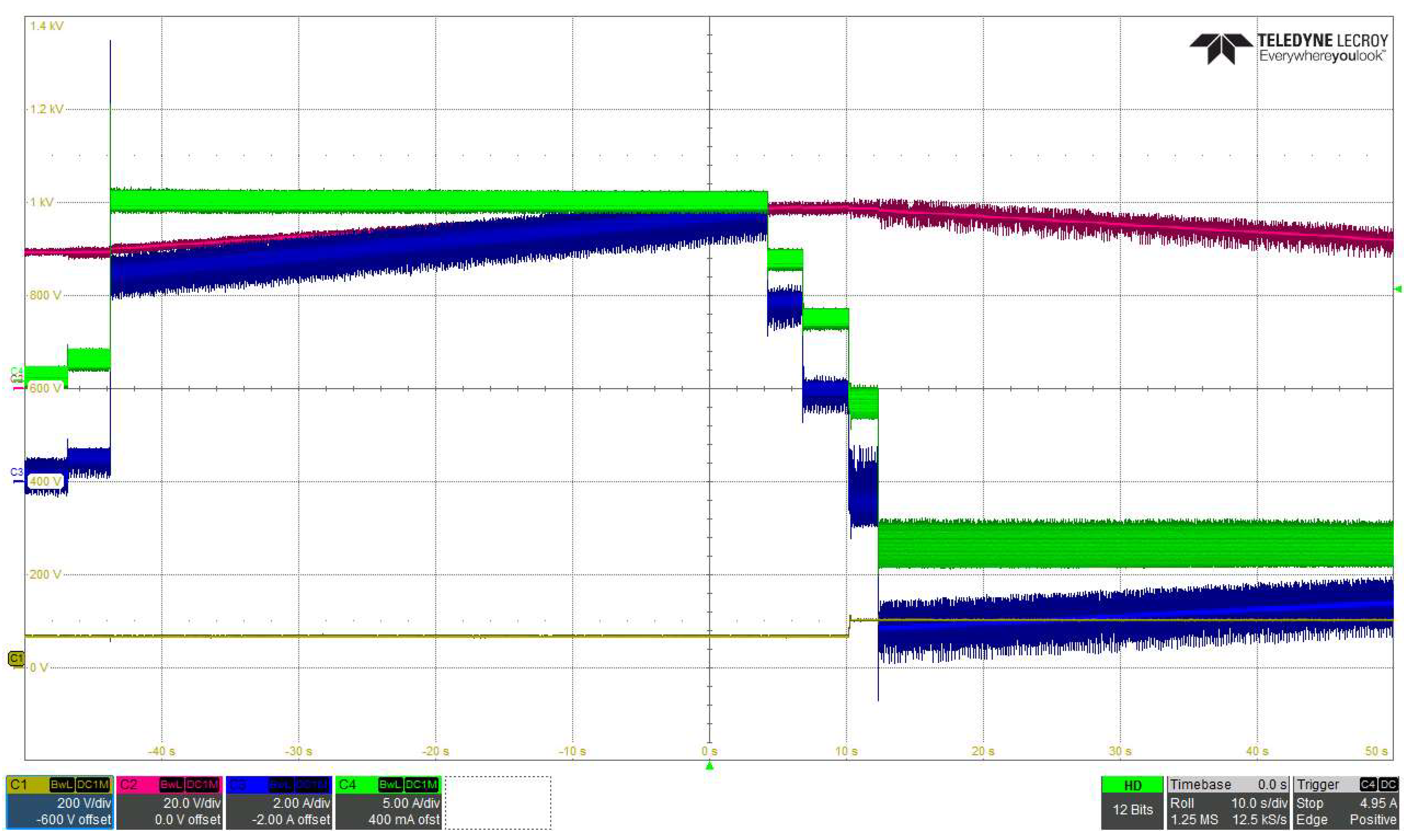
6. Experimental Results

A BHSC prototype, as shown in Figure 23, was built based on the information presented in the previous sections. The sizing of the converter’s passive components was performed according to the methodology presented in Section 3. The prototype parameters are listed in Table 2, Section 5, and Table 4.
The experimental setup used for testing the BHSC prototype is represented in Figure 24, and a picture of the setup is shown in Figure 25. A constant voltage electronic load was connected in parallel to the HV source to ensure the bidirectional operation. When the BHSC enters the step-up mode, the electronic load is automatically activated and takes the current from the VH port. When the converter is operating in the step-down mode, the electronic load is kept in standby.
A series of experimental tests were carried out to investigate the behavior of the prototype under different operating conditions. During these tests, the high-voltage source output was adjusted in the range of 100–300 V, and the voltage across the supercapacitors was between 20 and 80 V. The experimental results are presented in Figure 26, Figure 27, Figure 28, Figure 29, Figure 30 and Figure 31.
The first three results show key BHSC waveforms for steady-state operation. In Figure 26, the voltages across S3, S4, and S5 can be seen, together with the PWM driving signal for step-down operation at VH = 300 V and VL = 80 V, for a controlled current IL1 = 10 A. The interdependence between the PWM driving signal and the voltages on the three transistors corresponds to the description in Section 2. The voltage across the switched-capacitor cell, VCsw, is presented in Figure 27 for step-down operation at VH = 125 V and VL = 40 V, for a controlled current IL1 = 10 A. The two inductor currents are also displayed in the figure. The VCsw waveform can be compared to the theoretical waveform from Figure 5, which is similar; moreover, the correlation between iL2 and VCsw can be seen in both the theoretical and experimental waveforms. Figure 28 presents the currents through and the voltages across the two inductors for steady-state step-down operation at VH = 300 V and VL = 80 V, with a controlled current IL1 = 10 A. Some oscillations due to the PCB parasitic elements can be seen compared with the theoretical waveforms from Figure 5, which is common in power electronics.
A transition from steady-state step-up operation at −10 A to steady-state step-down operation at +10 A is presented in Figure 29, for VH = 100 V and VL = 50 V. Figure 30 shows an inverse transition. The waveforms are similar to the simulation waveforms presented in Figure 22. The differences between the simulation and the experimental waveforms arise from the fact that at zero crossing of the controlled current, the BHSC prototype behaves slightly differently than its simulation model. There is a small overshoot of the controlled current and a fast damped oscillation—both completely acceptable—in Figure 29. A larger oscillation is present in the uncontrolled current (iL2), which can be resolved, if necessary, by advanced control techniques. For the step-down–step-up transition, the controlled current presents no overshoot, but a step change in the uncontrolled current can be seen, which can also be eliminated through advanced control techniques.
Figure 31 presents typical waveforms for supercapacitor charging and discharging, for VH = 100 V. The low voltage, VL, varies between 30 V and 45 V. This limited voltage range was chosen to reduce the acquisition time and the acquired data, but it is sufficient to prove the good operation of the BHSC converter. The IL1 current is controlled in steps from the maximum charging to the maximum discharging values. It can be seen that there are no oscillations at the transition from the step-down operating mode (i.e., charging mode) to the step-up mode if this transition is performed at low current, even if the current reference is changed in steps.

7. Conclusions

This article is focused on a bidirectional hybrid DC–DC converter topology derived from a bidirectional buck converter by inserting a bidirectional switched-capacitor cell composed of two capacitors and three active switches in its structure.
The BHSC can achieve a high voltage conversion ratio, which makes it appropriate for applications characterized by a large variation in the voltage at one input—for example supercapacitor energy conversion and storage.
In addition to the increased voltage conversion ratio, the advantages of this topology include smaller passive components, reduced ripple currents at both the low- and high-voltage sides, and a common ground between the two ports. All of these positive features are demonstrated in this article through theoretical analysis, comparisons with several converters presented in the form of graphs and charts, digital simulations, and experimental tests.
The BHSC’s stability was analyzed with an emphasis on the constraints on the passive components, to obtain a stable operation, theoretically proven and validated by digital simulations, before the actual construction of the converter prototype. The simulation results confirmed the performance and the stability of the BHSC converter. Extensive experimental tests were carried out, proving good operation in both directions and a rapid, smooth transition between them.

Author Contributions

Conceptualization, N.M., O.C. and D.H.; methodology, M.G. and D.H.; software, M.G. and D.H.; validation, O.C. and N.M.; formal analysis, D.H. and M.G.; investigation, M.G., O.C. and D.H.; resources, N.M. and O.C.; data curation, D.H. and M.G.; writing—original draft preparation, O.C. and M.G.; writing—review and editing, N.M. and D.H.; visualization, D.H. and M.G.; supervision, O.C. and N.M.; project administration, N.M.; funding acquisition, N.M. and O.C. All authors have read and agreed to the published version of the manuscript.

Funding

This research was partially funded by a grant of the Romanian Ministry of Research, Innovation, and Digitalization, project number PFE 26/30.12.2021, PERFORM-CDI@UPT100—The increasing of the performance of the Polytechnic University of Timișoara by strengthening the research, development, and technological transfer capacity in the field of “Energy, Environment and Climate Change” at the beginning of the second century of its existence, within Program 1—Development of the National System of Research and Development, Subprogram 1.2—Institutional Performance Institutional Development Projects—Excellence Funding Projects in RDI, PNCDI III.

Conflicts of Interest

The authors declare no conflict of interest. The funders had no role in the design of the study; in the collection, analyses, or interpretation of data; in the writing of the manuscript; or in the decision to publish the results.

References

  1. Berrueta, A.; Ursúa, A.; Martín, I.S.; Eftekhari, A.; Sanchis, P. Supercapacitors: Electrical characteristics, modeling, applications, and future trends. IEEE Access 2019, 7, 50869–50896. [Google Scholar] [CrossRef]
  2. Ariyarathna, T.; Kularatna, N.; Gunawardane, K.; Jayananda, D.; Steyn-Ross, D.A. Development of Supercapacitor Technology and Its Potential Impact on New Power Converter Techniques for Renewable Energy. IEEE J. Emerg. Sel. Top. Ind. Electron. 2021, 2, 267–276. [Google Scholar] [CrossRef]
  3. Navarro, G.; Torres, J.; Blanco, M.; Nájera, J.; Santos-Herran, M.; Lafoz, M. Present and Future of Supercapacitor Technology Applied to Powertrains, Renewable Generation and Grid Connection Applications. Energies 2021, 14, 3060. [Google Scholar] [CrossRef]
  4. Hulea, D.; Muntean, N.; Gireada, M.; Cornea, O. A Bidirectional Hybrid Switched-Capacitor DC-DC Converter with a High Voltage Gain. In Proceedings of the 2019 International Aegean Conference on Electrical Machines and Power Electronics (ACEMP) & 2019 International Conference on Optimization of Electrical and Electronic Equipment (OPTIM), Istanbul, Turkey, 27–29 August 2019; pp. 289–296. [Google Scholar] [CrossRef]
  5. Hulea, D.; Cornea, O.; Muntean, N.; Fahimi, B. A bidirectional hybrid switched inductor converter with wide voltage conversion range. IET Power Electron. 2021, 14, 1753–1767. [Google Scholar] [CrossRef]
  6. Elsayad, N.; Moradisizkoohi, H.; Mohammed, O.A. A new hybrid structure of a bidirectional DC-DC converter with high conversion ratios for electric vehicles. IEEE Trans. Veh. Technol. 2020, 69, 194–206. [Google Scholar] [CrossRef]
  7. Dahono, P.A.; Dahono, A. A family of modular multilevel bidirectional DC-DC converters for high voltage-ratio and low-ripple applications. In Proceedings of the 2020 IEEE Energy Conversion Congress and Exposition (ECCE), Detroit, MI, USA, 11–15 October 2020; pp. 3934–3940. [Google Scholar]
  8. Hosseini, S.H.; Ghazi, R.; Heydari-Doostabad, H. An extendable quadratic bidirectional DC–DC converter for V2G and G2V applications. IEEE Trans. Ind. Electron. 2021, 68, 4859–4869. [Google Scholar] [CrossRef]
  9. Rezaii, R.; Nilian, M.; Safayatullah; Alaql, F.; Batarseh, I. Design and Experimental Study of a High Voltage Gain Bidirectional DC-DC Converter for Electrical Vehicle Application. In Proceedings of the 2022 IEEE Applied Power Electronics Conference and Exposition (APEC), Houston, TX, USA, 20–24 March 2022; pp. 2058–2063. [CrossRef]
  10. Chakraborty, S.; Vu, H.-N.; Hasan, M.M.; Tran, D.-D.; Baghdadi, M.E.; Hegazy, O. DC-DC Converter Topologies for Electric Vehicles, Plug-in Hybrid Electric Vehicles and Fast Charging Stations: State of the Art and Future Trends. Energies 2019, 12, 1569. [Google Scholar] [CrossRef] [Green Version]
  11. Chen, T.; Zhang, X.-P.; Wang, J.; Li, J.; Wu, C.; Hu, M.; Bian, H. A Review on Electric Vehicle Charging Infrastructure Development in the UK. J. Mod. Power Syst. Clean Energy 2020, 8, 193–205. [Google Scholar] [CrossRef]
  12. González-Castaño, C.; Restrepo, C.; Flores-Bahamonde, F.; Rodriguez, J. A Composite DC-DC Converter Based on the Versatile Buck-Boost Topology for Electric Vehicle Applications. Sensors 2022, 22, 5409. [Google Scholar] [CrossRef]
  13. Zhang, H.; Chen, Y.; Park, S.-J.; Kim, D.-H. A Family of Bidirectional DC–DC Converters for Battery Storage System with High Voltage Gain. Energies 2019, 12, 1289. [Google Scholar] [CrossRef] [Green Version]
  14. Chen, B.-Z.; Liao, H.; Chen, L.; Chen, J.-F. Design and Implementation of the Bidirectional DC-DC Converter with Rapid Energy Conversion. Energies 2022, 15, 898. [Google Scholar] [CrossRef]
  15. He, M.; Liu, Y.; Liu, H.; Gu, D. Design and analysis of a new bidirectional DC-DC converter with a high voltage conversion ratio and low voltage stress for energy applications. In Proceedings of the 2020 12th IEEE PES Asia-Pacific Power and Energy Engineering Conference (APPEEC), Nanjing, China, 20–23 September 2020; pp. 1–6. [Google Scholar]
  16. Wang, Z.; Wang, P.; Li, B.; Ma, X.; Wang, P. A bidirectional DC-DC converter with high voltage conversion ratio and zero ripple current for battery energy storage system. IEEE Trans. Power Electron. 2020, 36, 8012–8027. [Google Scholar] [CrossRef]
  17. Ramirez-Carrillo, M.; Ortega-Cisneros, S.; Rosas-Caro, J.C.; Rivera, J.; Valdez-Resendiz, J.E.; Mayo-Maldonado, J.C.; Valderrabano-Gonzalez, A. A Step-Up Converter with Large Voltage Gain and Low Voltage Rating on Capacitors. Energies 2022, 15, 7944. [Google Scholar] [CrossRef]
  18. Cornea, O.; Andreescu, G.-D.; Muntean, N.; Hulea, D. Bidirectional Power Flow Control in a DC Microgrid Through a Switched-Capacitor Cell Hybrid DC–DC Converter. IEEE Trans. Ind. Electron. 2017, 64, 3012–3022. [Google Scholar] [CrossRef]
  19. Bhaskar, M.S.; Ramachandaramurthy, V.K.; Padmanaban, S.; Blaabjerg, F.; Ionel, D.M.; Mitolo, M.; Almakhles, D. Survey of DC-DC Non-Isolated Topologies for Unidirectional Power Flow in Fuel Cell Vehicles. IEEE Access 2020, 8, 178130–178166. [Google Scholar] [CrossRef]
  20. Forouzesh, M.; Siwakoti, Y.P.; Gorji, S.A.; Blaabjerg, F.; Lehman, B. Step-Up DC–DC Converters: A Comprehensive Review of Voltage-Boosting Techniques, Topologies, and Applications. IEEE Trans. Power Electron. 2017, 32, 9143–9178. [Google Scholar] [CrossRef]
  21. Ramos-Paja, C.A.; Bastidas-Rodriguez, J.D.; Trejos-Grisales, L.A. Sliding-Mode Control of Bidirectional Flyback Converters with Bus Voltage Regulation for Battery Interface. Computation 2022, 10, 125. [Google Scholar] [CrossRef]
  22. Wu, Y.-E.; Tai, C.-H. Novel Bidirectional Isolated DC/DC Converter with High Gain Ratio and Wide Input Voltage for Electric Vehicle Storage Systems. Batteries 2022, 8, 240. [Google Scholar] [CrossRef]
  23. Lin, B.-R. Analysis and Implementation of a Bidirectional Converter with Soft Switching Operation. Processes 2022, 10, 561. [Google Scholar] [CrossRef]
  24. Punna, S.; Mailugundla, R.; Salkuti, S.R. Design, Analysis and Implementation of Bidirectional DC–DC Converters for HESS in DC Microgrid Applications. Smart Cities 2022, 5, 433–454. [Google Scholar] [CrossRef]
  25. Pellitteri, F.; Di Dio, V.; Puccio, C.; Miceli, R. A Model of DC-DC Converter with Switched-Capacitor Structure for Electric Vehicle Applications. Energies 2022, 15, 1224. [Google Scholar] [CrossRef]
  26. Hirth, M.P.; Gules, R.; Font, C.H.I. A wide conversion ratio bidirectional modified SEPIC converter with non-dissipative current snubber. IEEE J. Emerg. Sel. Topics Power Electron. 2020, 9, 1350–1360. [Google Scholar] [CrossRef]
  27. Axelrod, B.; Berkovich, Y.; Beck, Y. Family of universal bidirectional DC–DC converters with an extended voltage gain. IET Power Electron. 2019, 12, 3562–3570. [Google Scholar] [CrossRef]
  28. Zhang, Y.; Liu, Q.; Li, J.; Sumner, M. A Common Ground Switched-Quasi-$Z$ -Source Bidirectional DC–DC Converter with Wide-Voltage-Gain Range for EVs With Hybrid Energy Sources. IEEE Trans. Ind. Electron. 2018, 65, 5188–5200. [Google Scholar] [CrossRef]
  29. Ahmad, A.; Singh, R.K.; Mahanty, R. Bidirectional quadratic converter for wide voltage conversion ratio. In Proceedings of the 2016 IEEE International Conference on Power Electronics, Drives and Energy Systems (PEDES), Trivandrum, India, 14–17 December 2016; pp. 1–5. [Google Scholar] [CrossRef]
  30. Hulea, D.; Fahimi, B.; Muntean, N.; Cornea, O. High Ratio Bidirectional Hybrid Switched Inductor Converter Using Wide Bandgap Transistors. In Proceedings of the 2018 20th European Conference on Power Electronics and Applications (EPE’18 ECCE Europe), Riga, Latvia, 17–21 September 2018; pp. P.1–P.10. [Google Scholar]
  31. Axelrod, B.; Berkovich, Y.; Ioinovici, A. Switched-Capacitor/Switched-Inductor Structures for Getting Transformerless Hybrid DC–DC PWM Converters. IEEE Trans. Circuits Syst. I Regul. Pap. 2008, 55, 687–696. [Google Scholar] [CrossRef]
  32. Muntean, N.; Cornea, O.; Pelan, O.; Lascu, C. Comparative evaluation of buck and hybrid buck DC-DC converters for automotive applications. In Proceedings of the 2012 15th International Power Electronics and Motion Control Conference (EPE/PEMC), Novi Sad, Serbia, 4–6 September 2012; pp. DS2b.3-1–DS2b.3-6. [Google Scholar]
  33. Li, S.; Smedley, K.M.; Caldas, D.R.; Martins, Y.W. A hybrid bidirectional DC-DC converter for dual-voltage automotive systems. In Proceedings of the 2017 IEEE Applied Power Electronics Conference and Exposition (APEC), Tampa, FL, USA, 26–30 March 2017; pp. 355–361. [Google Scholar]
  34. Tomar, P.S.; Sharma, A.K.; Hada, K. Energy storage in DC microgrid system using non-isolated bidirectional soft-switching DC/DC converter. In Proceedings of the 2017 6th International Conference on Computer Applications in Electrical Engineering-Recent Advances (CERA), Roorkee, India, 5–7 October 2017; pp. 439–444. [Google Scholar]
  35. Ardi, H.; Ajami, A.; Kardan, F.; Avilagh, S.N. Analysis and Implementation of a Nonisolated Bidirectional DC–DC Converter with High Voltage Gain. IEEE Trans. Ind. Electron. 2016, 63, 4878–4888. [Google Scholar]
  36. Cornea, O.; Hulea, D.; Muntean, N.; Andreescu, G.-D. Step-Down Switched-Inductor Hybrid DC-DC Converter for Small Power Wind Energy Conversion Systems with Hybrid Storage. IEEE Access 2020, 8, 136092–136107. [Google Scholar] [CrossRef]
Figure 1. The unidirectional step-down switched-capacitor cell [31].
Energies 16 01337 g001
Figure 2. The bidirectional hybrid switched-capacitor (BHSC) converter.
Energies 16 01337 g002
Figure 3. BHSC equivalent schematic during ton, in step-down operating mode.
Energies 16 01337 g003
Figure 4. BHSC equivalent schematic during toff, in step-down operating mode.
Energies 16 01337 g004
Figure 5. Main theoretical waveforms of the BHSC for steady-state, step-down operating mode.
Energies 16 01337 g005
Figure 6. Voltage conversion ratios for the compared DC–DC converters (converters 1–8 described in Table 1).
Energies 16 01337 g006
Figure 7. Total energy stored in inductors, as a function of the voltage conversion ratio (converters 1–8 described in Table 1).
Energies 16 01337 g007
Figure 8. Total energy stored in capacitors (converters 1–8 described in Table 1).
Energies 16 01337 g008
Figure 9. Total active switch stress, as function of the voltage conversion ratio (Converters 1–8 described in Table 1).
Energies 16 01337 g009
Figure 10. Radar chart with 5 axes: voltage conversion ratio (@D = 15%); number of components; total active switch stress; mean inductor energy; mean capacitor energy. (a) Chart of the conventional buck–boost converter. (b) Chart of the BHSC.
Energies 16 01337 g010
Figure 11. Radar chart with 5 axes: voltage conversion ratio (@D = 15%); number of components; total active switch stress; mean inductor energy; mean capacitor energy. (a) Chart of converter 3. (b) Chart of converter 4.
Energies 16 01337 g011
Figure 12. Radar chart with 5 axes: voltage conversion ratio (@D = 15%); number of components; total active switch stress; mean inductor energy; mean capacitor energy. (a) Chart of converter 5. (b) Chart of converter 6.
Energies 16 01337 g012
Figure 13. Radar chart with 5 axes: voltage conversion ratio (@D = 15%); number of components; total active switch stress; mean inductor energy; mean capacitor energy. (a) Chart of converter 7. (b) Chart of converter 8.
Energies 16 01337 g013
Figure 14. BHSC schematic with parasitic components, used for stability analysis.
Energies 16 01337 g014
Figure 15. Equivalent BHSC schematic, derived from Figure 14, for ton.
Energies 16 01337 g015
Figure 16. Equivalent BHSC schematic, derived from Figure 14, for toff.
Energies 16 01337 g016
Figure 17. The block diagram of the control loop.
Energies 16 01337 g017
Figure 18. Bode diagram of H1(s) and H2(s).
Energies 16 01337 g018
Figure 19. Bode diagram of H1(z) and H2(z).
Energies 16 01337 g019
Figure 20. Frequency response of the converter with the designed controller C(z) ∙ H1(z) (PM = 80 deg, ft = 1.29 kHz).
Energies 16 01337 g020
Figure 21. Simulation results for I L 1 * = ± 50 A , VH = 400 V, VL = 80 V.
Energies 16 01337 g021
Figure 22. Simulation results for I L 1 * = ± 10 A , VH = 400 V, VL = 80 V.
Energies 16 01337 g022
Figure 23. BHSC prototype.
Energies 16 01337 g023
Figure 24. Experimental setup used for BHSC prototype testing.
Energies 16 01337 g024
Figure 25. A picture of the experimental setup used for BHSC prototype testing.
Energies 16 01337 g025
Figure 26. Experimental BHSC waveforms for step-down operation at VH = 300 V, VL = 80 V, and IL = 10 A (controlled). C1: VS3; C2: VS4; C3: VS5; C4: PWM driving signal.
Energies 16 01337 g026
Figure 27. Experimental BHSC waveforms for step-down operation at VH = 125 V, VL = 40 V, and IL = 10 A (controlled). C1: Voltage across the switched-capacitor cell, VCsw; C2: PWM driving signal; C3: iL2; C4: iL1.
Energies 16 01337 g027
Figure 28. Experimental BHSC waveforms for step-down operation at VH = 300 V, VL = 80 V, and IL = 10 A (controlled). C1: VL2; C2: iL2; C3: VL1; C4: iL1.
Energies 16 01337 g028
Figure 29. Experimental BHSC waveforms. Transition from step-up operation at −10 A to step-down operation at +10 A. Operating conditions: VH = 100 V, VL = 50 V, IL1 = (+/−)10A (controlled), IL2 = 3.75A. C3: iL2; C4: iL1.
Energies 16 01337 g029
Figure 30. Experimental BHSC waveforms. Transition from step-down operation at +10 A to step-up operation at −10 A. Operating conditions: VH = 100 V, VL = 50 V, IL1 = (−/+)10 A (controlled), IL2 = 3.75 A. C3: iL2; C4: iL1.
Energies 16 01337 g030
Figure 31. Experimental BHSC waveforms. Supercapacitor charging/discharging. Operating conditions: VH = 100 V, VL = 30…45 V…30 V, IL1 is controlled in steps to charge and discharge the supercapacitor. C2: VL; C3: iL2; C4: iL1.
Energies 16 01337 g031
Table 1. The DC–DC converters used in the comparison.
Converter (x)Voltage Ratio
VL/VH
Inductor Energy
WLTot(x)
Capacitor Energy
WCTot(x
Total Device Stress
S(x)
1. Buck—Boost D I L V L ( V H V L ) 2 r i f V H I L V L ( 8 V H 8 V L + r i V H ) 16 r v f V H 2 I L V H
2. BHSC D 2 D Conv. (1) I L V L ( 4 V H 4 V L + r i V H ) 8 r v f V H 2 I L ( V H + V L )
3. [18,25]Conv. (2)Conv. (1)Conv. (2) I L ( V H + V L ) 2 V H
4. [5,13] *Conv. (2)Conv. (1) I L V L ( V H V L ) 2 r v f V H Conv. (3)
5. [26]Conv. (2)Conv. (1) I L V L ( 16 V H 2 8 V H V L + 8 V L 2 + r i V H ( V L + V H ) ) 16 r v f V H ( V H + V L ) Conv. (3)
6. [27]Conv. (2)Conv. (1)Conv. (4) 3 I L ( V H + V L ) 2 2 V H
7. [28]Conv. (2) I L V L ( 3 V H 2 2 V H V L V L 2 ) 4 r i f V H ( V H + V L ) I L V L ( V H V L + r i ( V H + V L ) / 16 ) r v f ( V H + V L ) Conv. (3)
8. [29] D 2 I L V L V H 1 / 2 V L 1 / 2 r i f V H 1 / 2 I L V L ( V H 1 / 2 V L 1 / 2 + r i V H 1 / 2 / 16 ) r v f V H 1 / 2 4 I L V H 1 / 2 V L 1 / 2
* Topology III.
Table 2. BHSC stability analysis prototype characteristics.
Specifications
PartValueUnitESRESR ValueUnitComponent
L168 × 2µHRL112 × 2mΩ2xDEHF-42/0,068/40
L2470µHRL253mΩDEHF-42/0,47/16
Csw330 × 3µFRCsw214.7/3mΩALC80A331CD350
CL330 × 3µFRCL452/3mΩSLP331M160A1P3
CH100 × 3mFRCH1.493/3SLPX101M400A3P3
Table 3. The poles and zeroes of H1(s) and H2(s).
ElementPole and Zero Values
H1(s) Poles −4.509641064e+03, −3.584847675e+03, −5.924218847e+02 +1.802230478e+03i,
−5.924218847e+02 −1.802230478e+03i, −9.720039549e+02
H1(s) Zeros −4647.704034, −3603.028284, −569.9738229 +1825.663084i,
−569.9738229–1825.663084i
H2(s) Poles −4.509641064e+03, −3.584847675e+03, −5.924218847e+02 +1.802230478e+03i,
−5.924218847e+02 −1.802230478e+03i, −9.720039549e+02
H2(s) Zeros −4523.253666, −3932.363350, −670.2071775 + 1708.298882i,
−670.2071775–1708.298882i
Table 4. BHSC prototype parameters.
Specifications
ElementValueUnitDescription
P3.25kWNominal converter power
VL0–80VLow voltage value
VH100–325VHigh voltage value
IL33ANominal current on the low-voltage input
IH12ANominal current on the high-voltage input
f80kHzSwitching frequency
Disclaimer/Publisher’s Note: The statements, opinions and data contained in all publications are solely those of the individual author(s) and contributor(s) and not of MDPI and/or the editor(s). MDPI and/or the editor(s) disclaim responsibility for any injury to people or property resulting from any ideas, methods, instructions or products referred to in the content.

