
Preparation and Numerical Optimization of TiO2:CdS Thin Films in Double Perovskite Solar Cell
 , ,
, ,  , ,
, ,  and
and
Abstract
:
1. Introduction
2. Experimental
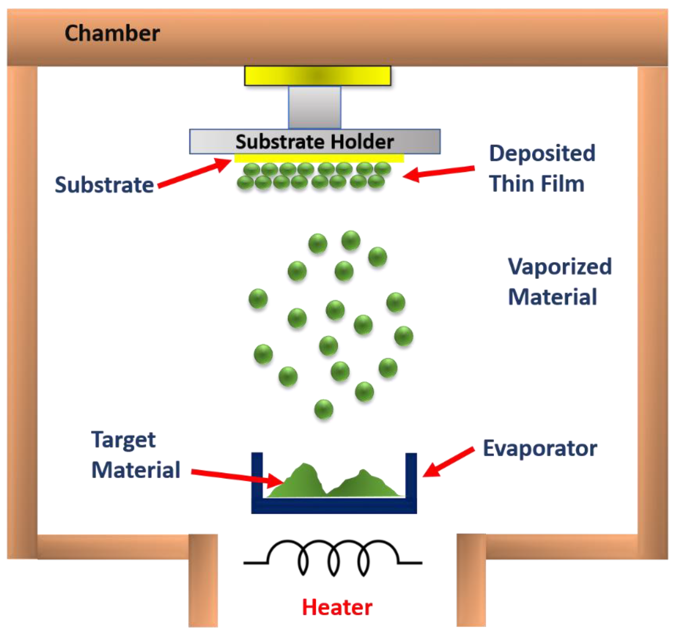
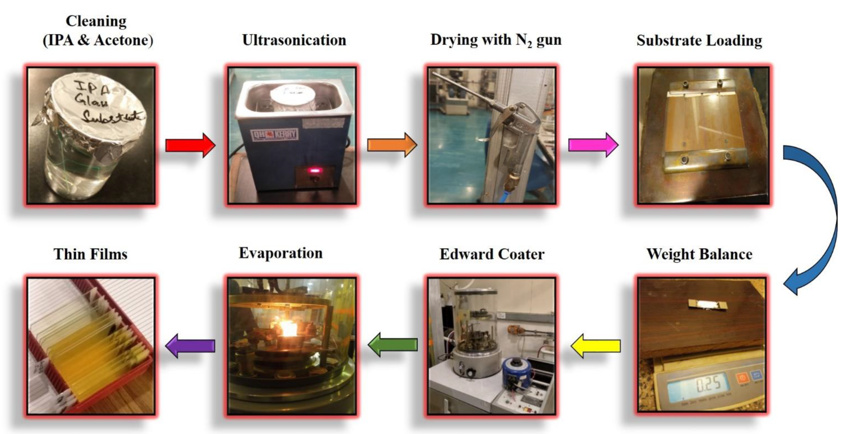
2.1. Sample Preparation
2.2. Characterization
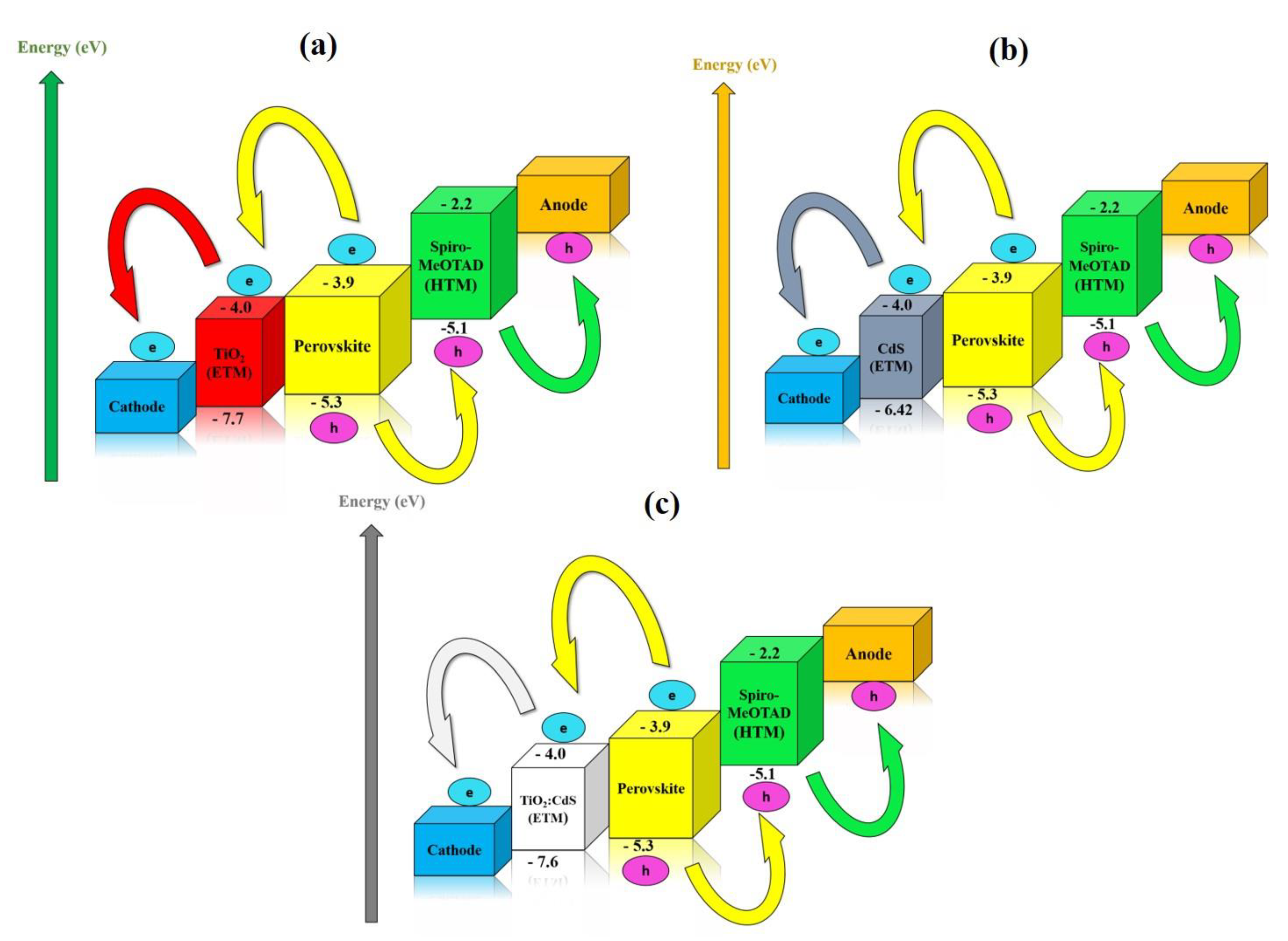
3. Numerical Modeling of Double Perovskite Solar Cell
4. Results and Discussion
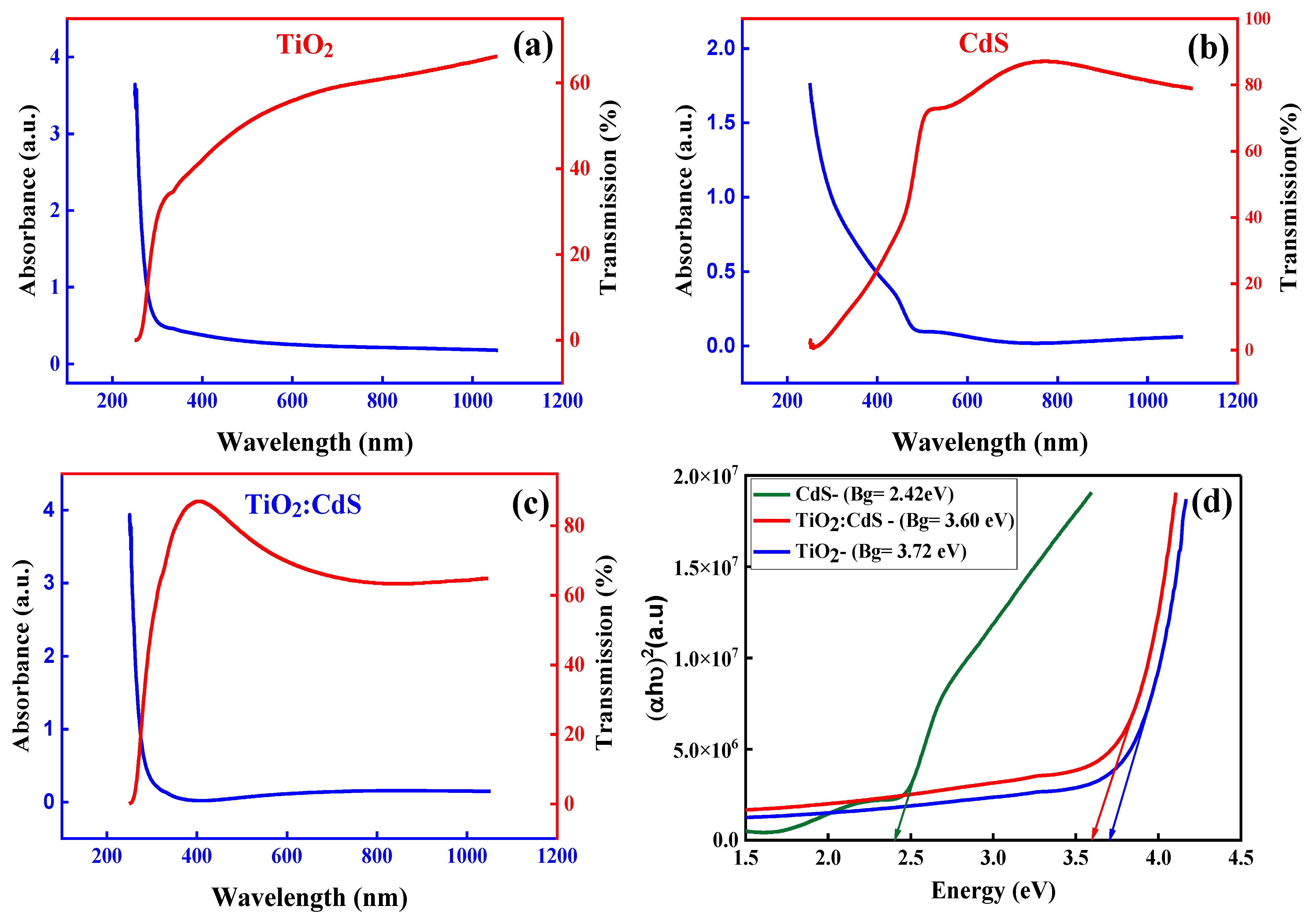
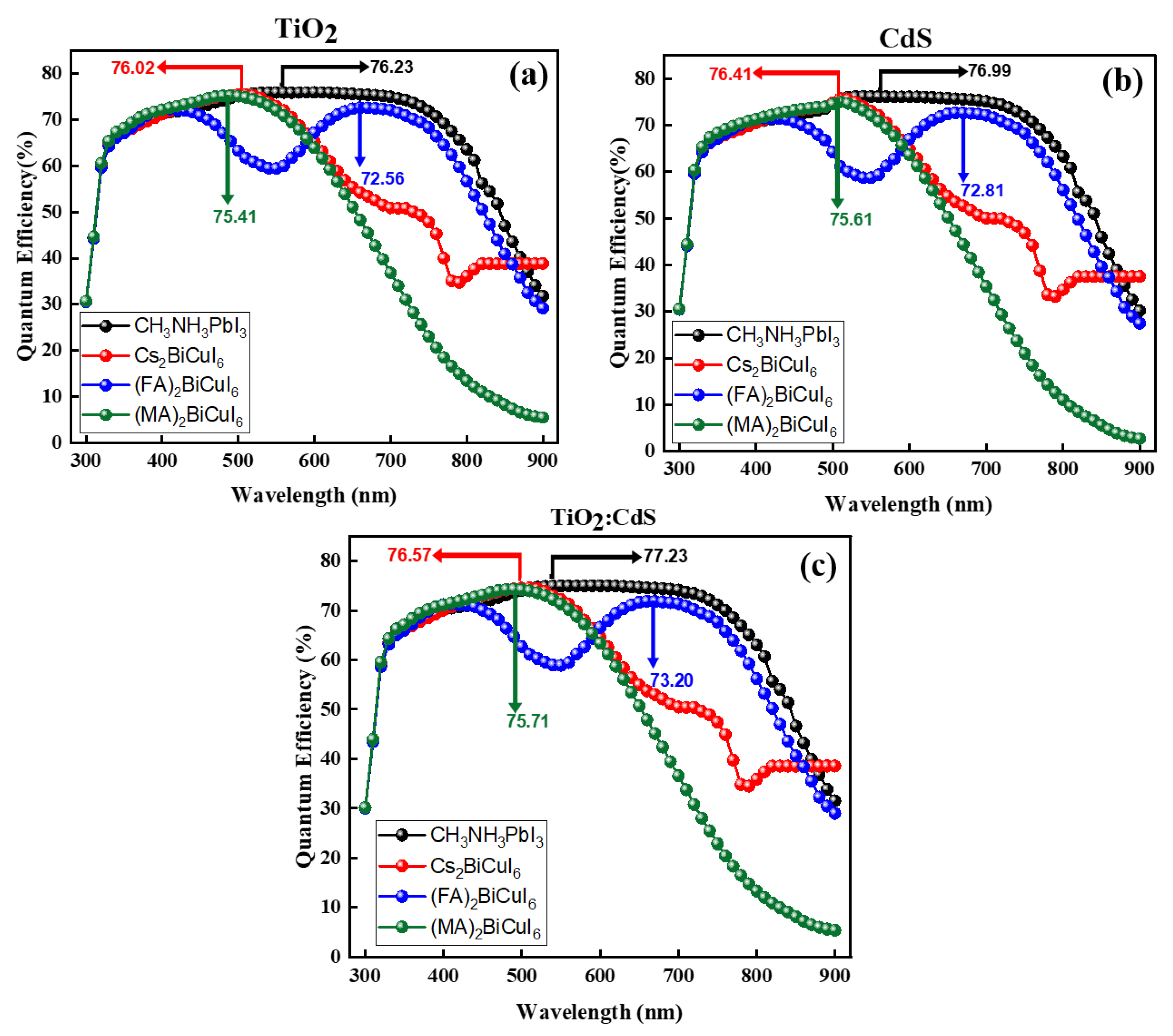
4.1. UV-Vis Results
Tauc Plot
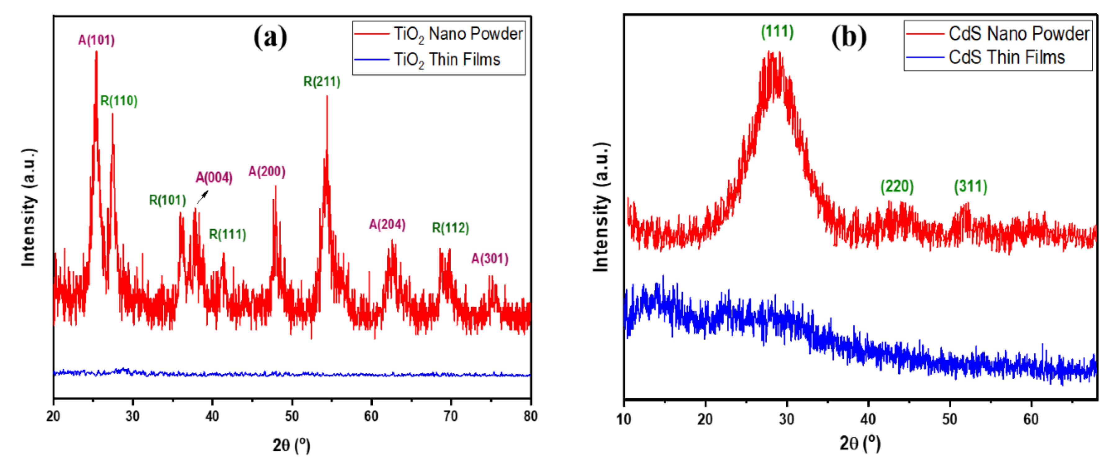
4.2. XRD Analysis
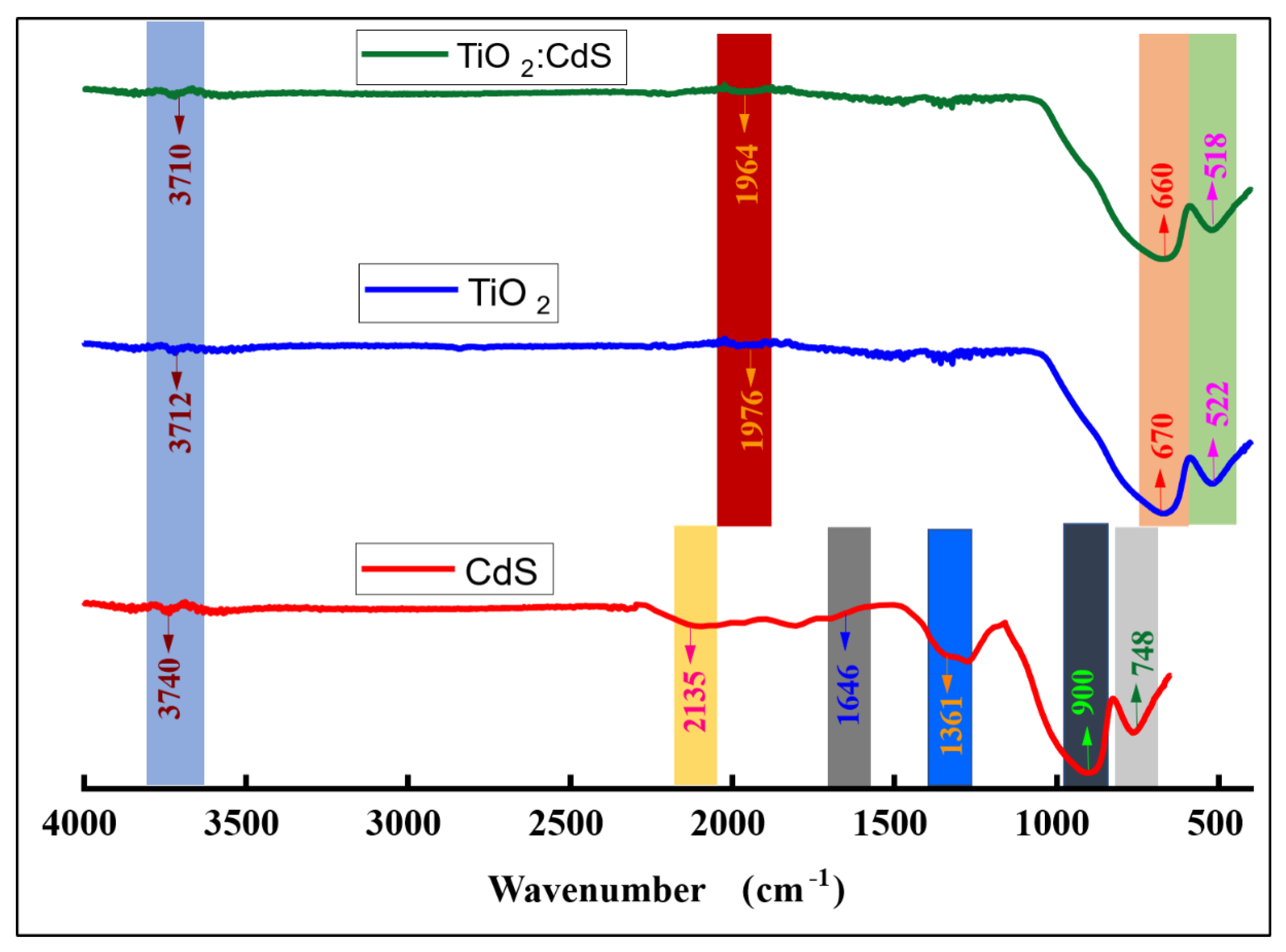
4.3. FTIR Results
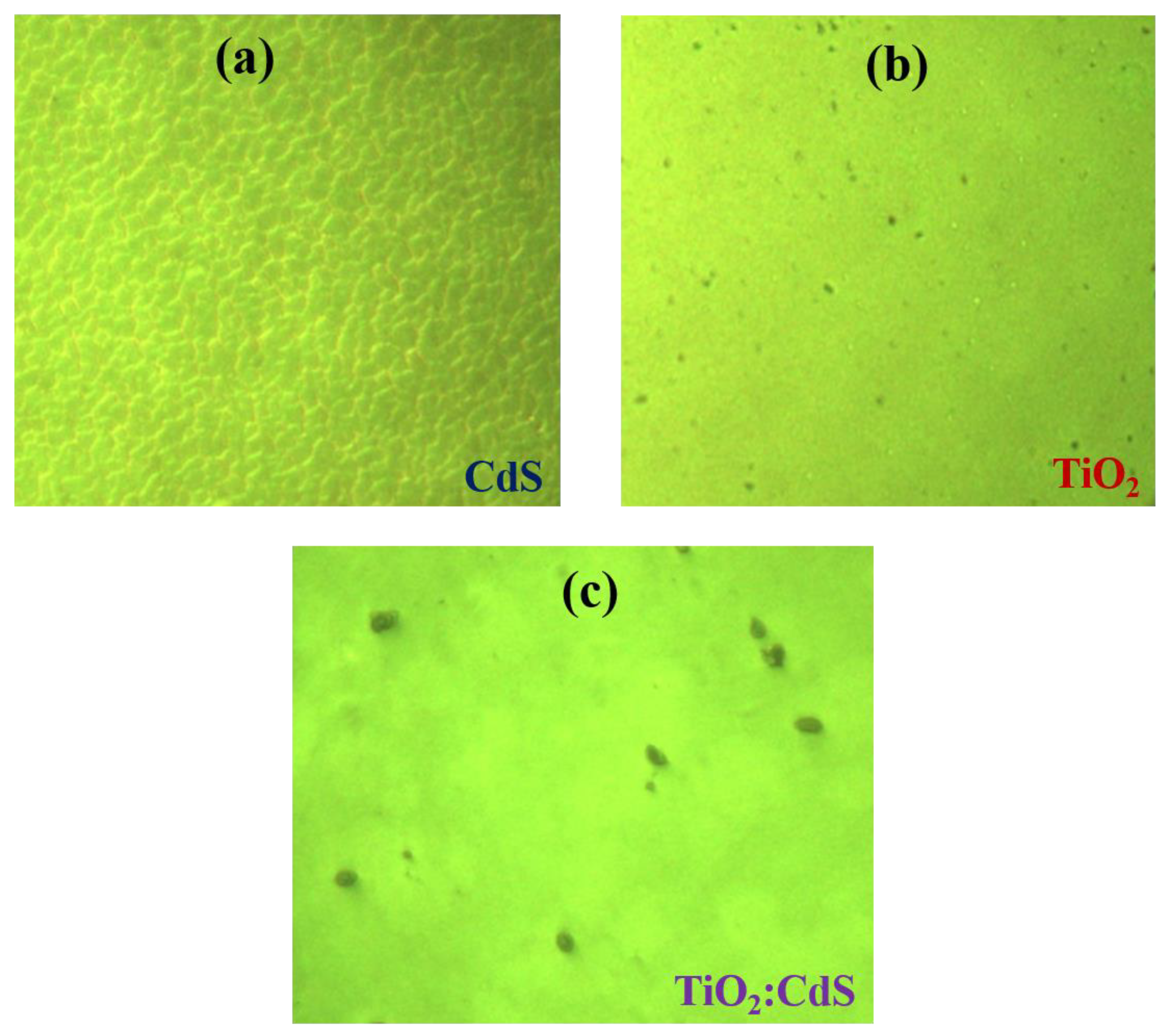
4.4. Optical Microscopy
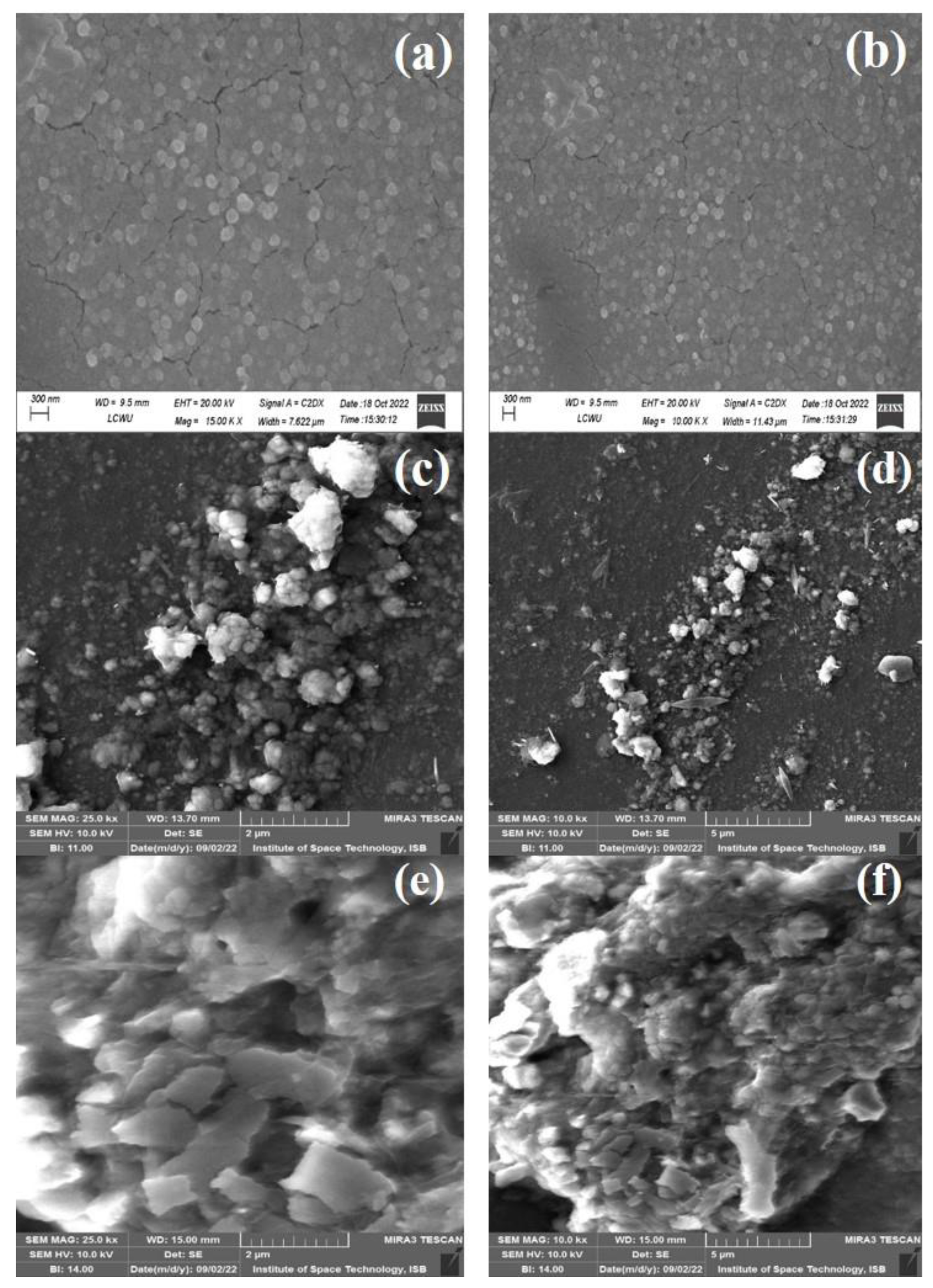
4.5. SEM Analysis
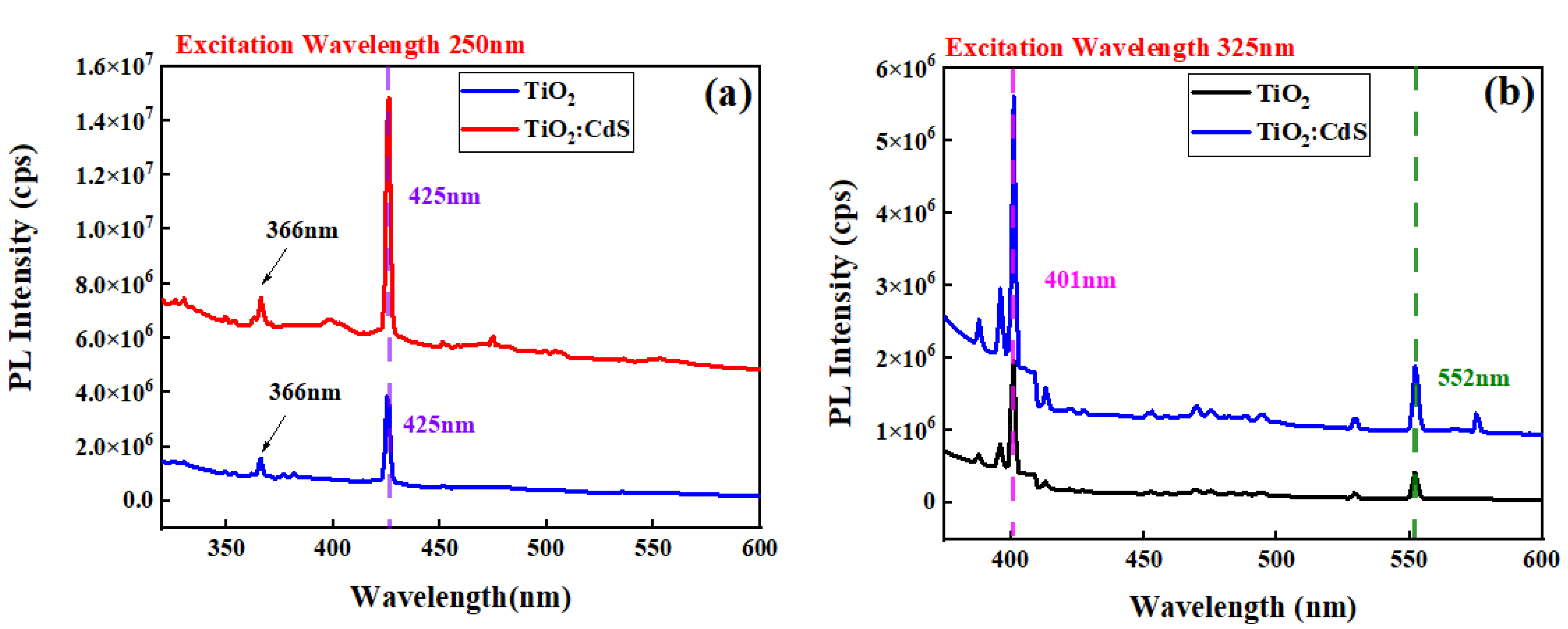
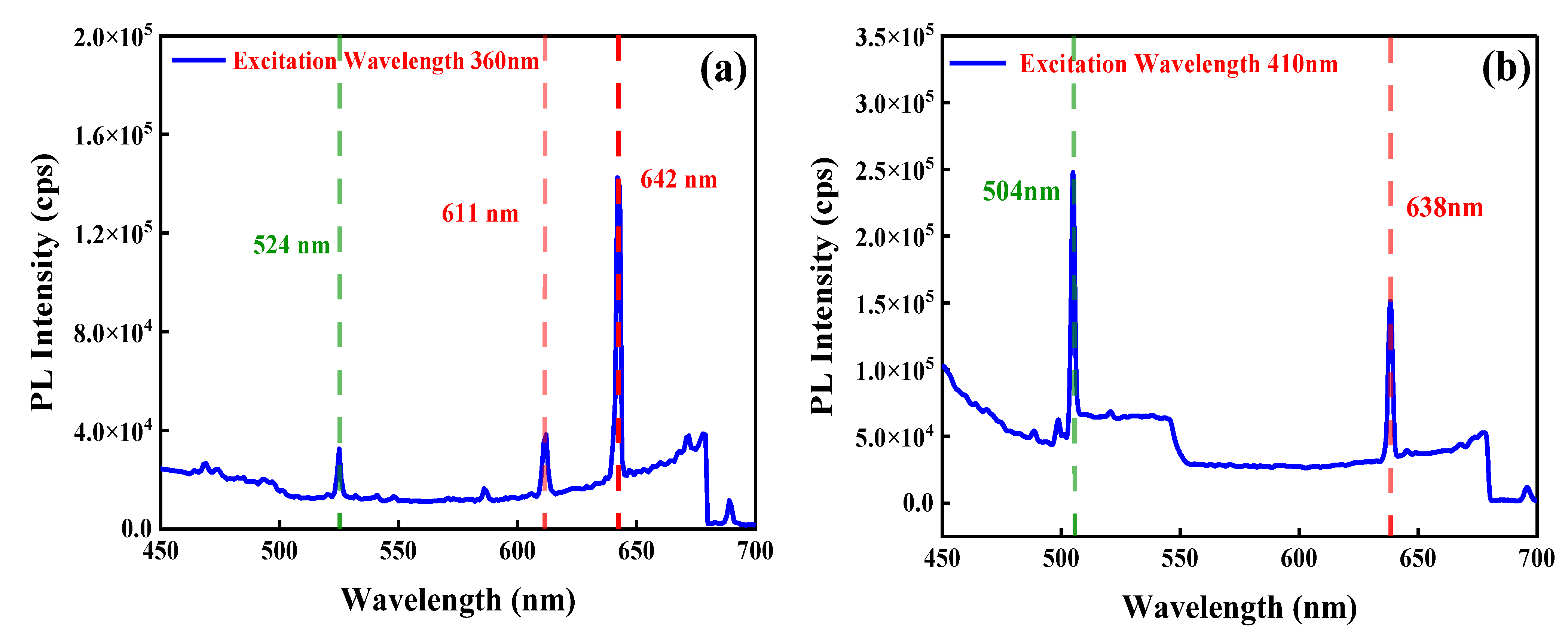
4.6. Photoluminescence (PL) Analysis
4.7. Resistivity Measurement
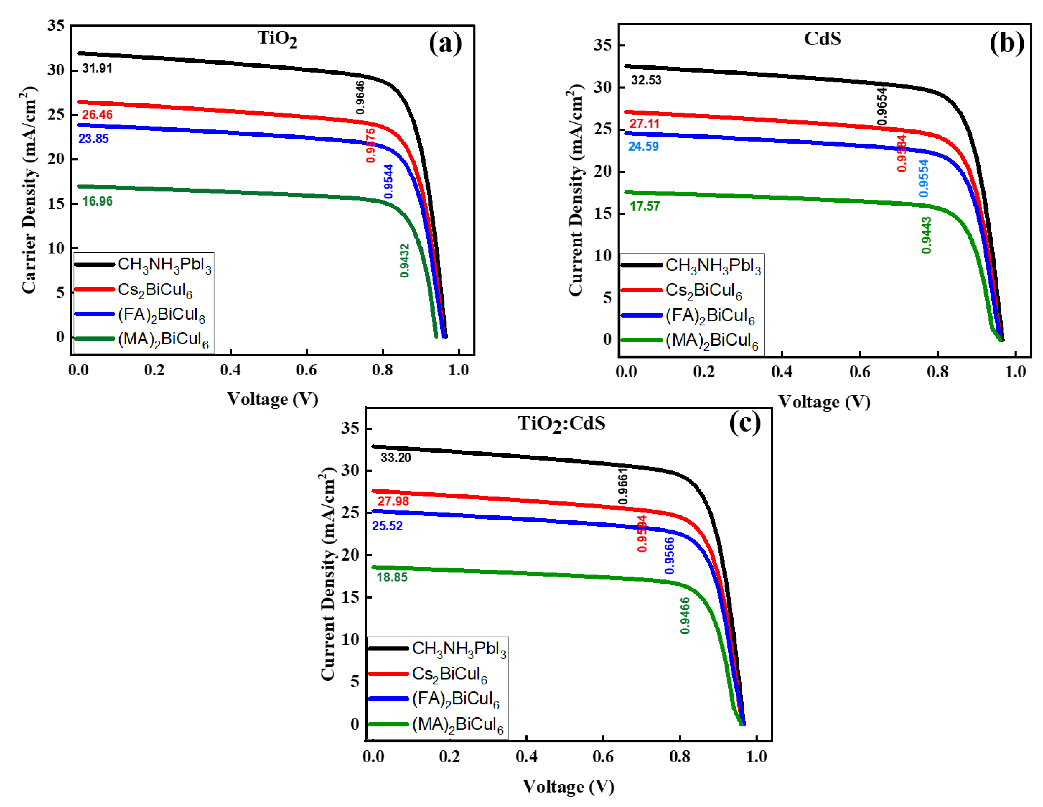
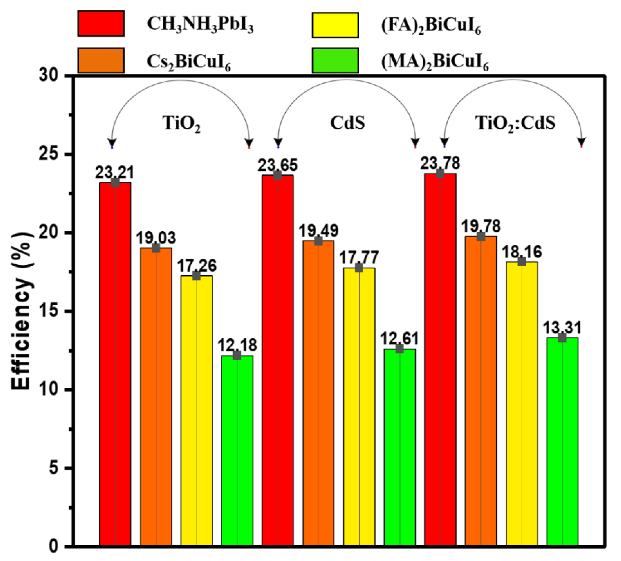
4.8. J–V Comparison between Different ETMs and Perovskite Materials

| Parameters | FTO [36,41,43,82] | TiO2, CdS, TiO2:CdS [41,43,82,85] | Perovskite [26,39,41,43,82,87] | Spiro-MeOTAD [36,39,41,43] |
|---|---|---|---|---|
| Thickness (nm) | 200 | 50, 50, 50 | 200 | 150 |
| Acceptor Density | 0 | 0, 0, 0 | 0 | |
| Donor Density | 1019 | 1017, 1017, 1018 | 1017 | 0 |
| Bandgap (eV) | 3.5 | 3.72, 2.42, 3.6 | 1.6 | 2.9 |
| Relative Dielectric Permittivity | 9 | 10, 10, 13 | 6.5 | 3 |
| Mobility of Electron (cm2/Vs) | 20 | 20, 100, 35 | 2 | |
| Mobility of Hole (cm2/Vs) | 10 | 10, 25, 15 | 2 | |
| Electron Affinity (eV) | 4 | 4, 4, 4 | 3.9 | 2.2 |
| Defect Density | , |
| Interface Defect Density [36,39,41] | |
|---|---|
| IL1 (ETL/Active Layer) Defect Density IL2 (Active Layer/HTL) Defect Density | 2 × 109 cm−2 2 × 109 cm−2 |
| Back Metal Contact Properties [39,40,41] | |
| The electron work function of Au Surface recombination velocity of the electron Surface recombination velocity of hole | −5.1 eV 105 cm/s 107 cm/s |
| Front Metal Contact Properties [39,40,41] | |
| The electron work function of TCO Surface recombination velocity electron Surface recombination velocity of hole | −4.4 eV 107 cm/s 105 cm/s |
5. Conclusions
Author Contributions
Funding
Data Availability Statement
Acknowledgments
Conflicts of Interest
Abbreviations
References
- Bhatti, M.A.; Shah, A.A.; Almaani, K.F.; Tahira, A.; Chandio, A.D.; Willander, M.; Nur, O.; Mugheri, A.Q.; Bhatti, A.L.; Waryani, B.; et al. TiO2/ZnO Nanocomposite Material for Efficient Degradation of Methylene Blue. J. Nanosci. Nanotechnol. 2021, 21, 2511–2519. [Google Scholar] [CrossRef]
- Bhatti, M.A.; Gilani, S.J.; Shah, A.A.; Channa, I.A.; Almani, K.F.; Chandio, A.D.; Halepoto, I.A.; Tahira, A.; Bin Jumah, M.N.; Ibupoto, Z.H. Effective Removal of Methylene Blue by Surface Alteration of TiO2 with Ficus Carica Leaf Extract under Visible Light. Nanomaterials 2022, 12, 2766. [Google Scholar] [CrossRef]
- Hoffmann, M.R.; Martin, S.T.; Choi, W.; Bahnemann, D.W. Environmental applications of semiconductor photocatalysis. Chem. Rev. 1995, 95, 69–96. [Google Scholar] [CrossRef]
- Thompson, T.L.; Yates, J.T. Surface science studies of the photoactivation of TiO2 new photochemical processes. Chem. Rev. 2006, 106, 4428–4453. [Google Scholar] [CrossRef]
- Tan, J.; Liu, L.; Li, F.; Chen, Z.; Chen, G.Y.; Fang, F.; Jinsong, G.; Miao, H.; Xiaohong, Z. Screening of Endocrine Disrupting Potential of Surface Waters via an Affinity-Based Biosensor in a Rural Community in the Yellow River Basin, China. Environ. Sci. Technol. 2022, 56, 14350–14360. [Google Scholar]
- Baron Jaimes, A.; Jaramillo-Quintero, O.A.; Miranda Gamboa, R.A.; Medina-Flores, A.; Rincon, M.E. Functional ZnO/TiO2 Bilayer as Electron Transport Material for Solution-Processed Sb2S3 Solar Cells. Sol. RRL 2021, 5, 2000764. [Google Scholar] [CrossRef]
- Li, H.; Wang, X.; Xu, J.; Zhang, Q.; Bando, Y.; Golberg, D.; Ma, Y.; Zhai, T. One-dimensional CdS nanostructures: A promising candidate for optoelectronics. Adv. Mater. 2013, 25, 3017–3037. [Google Scholar] [CrossRef]
- Hullavarad, N.; Karulkar, P. Cadmium sulphide (CdS) nanotechnology: Synthesis and applications. J. Nanosci. Nanotechnol. 2008, 8, 3272–3299. [Google Scholar] [CrossRef]
- Müller, J.; Kluth, O.; Wieder, S.; Siekmann, H.; Schöpe, G.; Reetz, W.; Vetterl, O.; Lundszien, D.; Lambertz, A.; Finger, F.; et al. Development of highly efficient thin film silicon solar cells on texture-etched zinc oxide-coated glass substrates. Sol. Energy Mater. Sol. Cells 2001, 66, 275–281. [Google Scholar] [CrossRef]
- Yu, F. Internal Polarization Effect in Perovskite Solar Cells; University of Pittsburgh: Pittsburgh, PA, USA, 2016. [Google Scholar]
- Conings, B.; Baeten, L.; Jacobs, T.; Dera, R.; D’Haen, J.; Manca, J.; Boyen, H.G. An easy-to-fabricate low-temperature TiO2 electron collection layer for high efficiency planar heterojunction perovskite solar cells. APL Mater. 2014, 2, 081505. [Google Scholar] [CrossRef]
- Liu, D.; Kelly, T.L. Perovskite solar cells with a planar heterojunction structure prepared using room-temperature solution processing techniques. Nat. Photonics 2014, 8, 133–138. [Google Scholar] [CrossRef]
- Kojima, A.; Teshima, K.; Miyasaka, T.; Shirai, Y. Novel photoelectrochemical cell with mesoscopic electrodes sensitized by lead-halide compounds (2). In ECS Meeting Abstracts; IOP Publishing: Bristol, UK, 2006. [Google Scholar]
- Kojima, A.; Teshima, K.; Shirai, Y.; Miyasaka, T. Organometal halide perovskites as visible-light sensitizers for photovoltaic cells. J. Am. Chem. Soc. 2009, 131, 6050–6051. [Google Scholar] [CrossRef] [PubMed]
- Im, J.H.; Lee, C.R.; Lee, J.W.; Park, S.W.; Park, N.G. 6.5% efficient perovskite quantum-dot-sensitized solar cell. Nanoscale 2011, 3, 4088–4093. [Google Scholar] [CrossRef] [Green Version]
- Anttu, N. Shockley–Queisser detailed balance efficiency limit for nanowire solar cells. ACS Photonics 2015, 2, 446–453. [Google Scholar] [CrossRef]
- Sha, W.E.; Ren, X.; Chen, L.; Choy, W.C. The efficiency limit of CH3NH3PbI3 perovskite solar cells. Appl. Phys. Lett. 2015, 106, 221104. [Google Scholar] [CrossRef] [Green Version]
- Law, M.; Greene, L.E.; Johnson, J.C.; Saykally, R.; Yang, P. Nanowire dye-sensitized solar cells. Nat. Mater. 2005, 4, 455–459. [Google Scholar] [CrossRef]
- Lv, Y.; Cai, B.; Wu, Y.; Wang, S.; Jiang, Q.; Ma, Q.; Liu, J.J.; Zhang, W.H. High performance perovskite solar cells using TiO2 nanospindles as ultrathin mesoporous layer. J. Energy Chem. 2018, 27, 951–956. [Google Scholar] [CrossRef] [Green Version]
- Yang, G.; Tao, H.; Qin, P.; Ke, W.; Fang, G. Recent progress in electron transport layers for efficient perovskite solar cells. J. Mater. Chem. A 2016, 4, 3970–3990. [Google Scholar] [CrossRef]
- Jeon, N.J.; Noh, J.H.; Kim, Y.C.; Yang, W.S.; Ryu, S.; Seok, S.I. Solvent engineering for high-performance inorganic–organic hybrid perovskite solar cells. Nat. Mater. 2014, 13, 897–903. [Google Scholar] [CrossRef]
- Yang, W.S.; Noh, J.H.; Jeon, N.J.; Kim, Y.C.; Ryu, S.; Seo, J.; Seok, S.I. High-performance photovoltaic perovskite layers fabricated through intramolecular exchange. Science 2015, 348, 1234–1237. [Google Scholar] [CrossRef]
- Song, J.; Zheng, E.; Bian, J.; Wang, X.F.; Tian, W.; Sanehira, Y.; Miyasaka, T. Low-temperature SnO2-based electron selective contact for efficient and stable perovskite solar cells. J. Mater. Chem. A 2015, 3, 10837–10844. [Google Scholar] [CrossRef]
- Kumar, M.H.; Yantara, N.; Dharani, S.; Graetzel, M.; Mhaisalkar, S.; Boix, P.P.; Mathews, N. Flexible, low-temperature, solution processed ZnO-based perovskite solid state solar cells. Chem. Commun. 2013, 49, 11089–11091. [Google Scholar] [CrossRef]
- Son, D.Y.; Im, J.H.; Kim, H.S.; Park, N.G. 11% efficient perovskite solar cell based on ZnO nanorods: An effective charge collection system. J. Phys. Chem. C 2014, 118, 16567–16573. [Google Scholar] [CrossRef]
- Mali, S.S.; Shim, C.S.; Kim, H.; Patil, P.S.; Hong, C.K. In situ processed gold nanoparticle-embedded TiO2 nanofibers enabling plasmonic perovskite solar cells to exceed 14% conversion efficiency. Nanoscale 2016, 8, 2664–2677. [Google Scholar] [CrossRef]
- Shin, S.S.; Yeom, E.J.; Yang, W.S.; Hur, S.; Kim, M.G.; Im, J.; Seo, J.; Noh, J.H.; Seok, S.I. Colloidally prepared La-doped BaSnO3 electrodes for efficient, photostable perovskite solar cells. Science 2017, 356, 167–171. [Google Scholar] [CrossRef]
- Zhu, J.; Liu, X.; Geier, M.L.; McMorrow, J.J.; Jariwala, D.; Beck, M.E.; Huang, W.; Marks, T.J.; Hersam, M.C. Layer-by-layer assembled 2D montmorillonite dielectrics for solution-processed electronics. Adv. Mater. 2016, 28, 63–68. [Google Scholar] [CrossRef]
- Xie, H.; Yin, X.; Liu, J.; Guo, Y.; Chen, P.; Que, W.; Wang, G.; Gao, B. Low temperature solution-derived TiO2-SnO2 bilayered electron transport layer for high performance perovskite solar cells. Appl. Surf. Sci. 2019, 464, 700–707. [Google Scholar] [CrossRef]
- Xu, X.; Zhang, H.; Shi, J.; Dong, J.; Luo, Y.; Li, D.; Meng, Q. Highly efficient planar perovskite solar cells with a TiO2/ZnO electron transport bilayer. J. Mater. Chem. A 2015, 3, 19288–19293. [Google Scholar] [CrossRef]
- Chai, W.; Zhu, W.; Chen, D.; Chen, D.; Xi, H.; Chang, J.; Zhang, J.; Zhang, C.; Hao, Y. Combustion-processed NiO/ALD TiO2 bilayer as a novel low-temperature electron transporting material for efficient all-inorganic CsPbIBr2 solar cell. Sol. Energy 2020, 203, 10–18. [Google Scholar] [CrossRef]
- Dunlap-Shohl, W.A.; Younts, R.; Gautam, B.; Gundogdu, K.; Mitzi, D.B. Effects of Cd diffusion and doping in high-performance perovskite solar cells using CdS as electron transport layer. J. Phys. Chem. C 2016, 120, 16437–16445. [Google Scholar] [CrossRef]
- Wessendorf, C.D.; Hanisch, J.; Müller, D.; Ahlswede, E. CdS as Electron Transport Layer for Low-Hysteresis Perovskite Solar Cells. Sol. RRL 2018, 2, 1800056. [Google Scholar] [CrossRef]
- Luo, C.; Jiang, P.; Hu, L.; Bian, M.; Wan, L.; Niu, H.; Mao, X.; Zhou, R.; Xu, J. Constructing CdS-Based Electron Transporting Layers With Efficient Electron Extraction for Perovskite Solar Cells. IEEE J. Photovolt. 2021, 11, 1014–1021. [Google Scholar] [CrossRef]
- Gu, Z.; Chen, F.; Zhang, X.; Liu, Y.; Fan, C.; Wu, G.; Li, H.; Chen, H. Novel planar heterostructure perovskite solar cells with CdS nanorods array as electron transport layer. Sol. Energy Mater. Sol. Cells 2015, 140, 396–404. [Google Scholar] [CrossRef]
- Lin, L.; Jiang, L.; Qiu, Y.; Yu, Y. Modeling and analysis of HTM-free perovskite solar cells based on ZnO electron transport layer. Superlattices Microstruct. 2017, 104, 167–177. [Google Scholar] [CrossRef]
- Chakraborty, K.; Choudhury, M.G.; Paul, S. Numerical study of Cs2TiX6 (X = Br−, I−, F− and Cl−) based perovskite solar cell using SCAPS-1D device simulation. Sol. Energy 2019, 194, 886–892. [Google Scholar] [CrossRef]
- Karthick, S.; Velumani, S.; Bouclé, J. Experimental and SCAPS simulated formamidinium perovskite solar cells: A comparison of device performance. Sol. Energy 2020, 205, 349–357. [Google Scholar] [CrossRef]
- Nowsherwan, G.A.; Hussain, S.S.; Khan, M.; Haider, S.; Akbar, I.; Nowsherwan, N.; Ikram, S.; Ishtiaq, S.; Riaz, S.; Naseem, S. Role of graphene-oxide and reduced-graphene-oxide on the performance of lead-free double perovskite solar cell. Zeitschrift für Naturforschung A 2022, 77, 1083–1098. [Google Scholar] [CrossRef]
- Abdelaziz, S.; Zekry, A.; Shaker, A.; Abouelatta, M. Investigating the performance of formamidinium tin-based perovskite solar cell by SCAPS device simulation. Opt. Mater. 2020, 101, 109738. [Google Scholar] [CrossRef]
- Hussain, S.S.; Riaz, S.; Nowsherwan, G.A.; Jahangir, K.; Raza, A.; Iqbal, M.J.; Sadiq, I.; Hussain, S.M.; Naseem, S. Numerical modeling and optimization of lead-free hybrid double perovskite solar cell by using SCAPS-1D. J. Renew. Energy 2021, 2021, 6668687. [Google Scholar] [CrossRef]
- Kumar, M.; Raj, A.; Kumar, A.; Anshul, A. An optimized lead-free formamidinium Sn-based perovskite solar cell design for high power conversion efficiency by SCAPS simulation. Opt. Mater. 2020, 108, 110213. [Google Scholar] [CrossRef]
- Samiul Islam, M.; Sobayel, K.; Al-Kahtani, A.; Islam, M.A.; Muhammad, G.; Amin, N.; Shahiduzzaman, M.; Akhtaruzzaman, M. Defect study and modelling of SnX3-based perovskite solar cells with SCAPS-1D. Nanomaterials 2021, 11, 1218. [Google Scholar] [CrossRef]
- Haider, S.Z.; Anwar, H.; Wang, M. A comprehensive device modelling of perovskite solar cell with inorganic copper iodide as hole transport material. Semicond. Sci. Technol. 2018, 33, 035001. [Google Scholar] [CrossRef] [Green Version]
- Chen, W.-K. Fundamentals of Circuits and Filters; CRC Press: Boca Raton, FL, USA, 2018. [Google Scholar]
- Lisičar Vukušić, J. Multidisciplinary Approach in Industrial Baker′ s Yeast Production: From Manufacture to Integrated Sustainability; Institutionelles Repositorium der Leibniz Universität Hannover: Hannover, Germany, 2019. [Google Scholar]
- Förster, H. UV/vis spectroscopy. Molecular Sieves—Science and Technology; Characterization I; Springer: Berlin/Heidelberg, Germany, 2004; pp. 337–426. [Google Scholar]
- Picollo, M.; Aceto, M.; Vitorino, T. UV-Vis spectroscopy. Phys. Sci. Rev. 2019, 4. [Google Scholar] [CrossRef]
- Ennaoui, A.; Sankapal, B.R.; Skryshevsky, V.; Lux-Steiner, M.C. TiO2 and TiO2–SiO2 thin films and powders by one-step soft-solution method: Synthesis and characterizations. Sol. Energy Mater. Sol. Cells 2006, 90, 1533–1541. [Google Scholar] [CrossRef]
- Purkayastha, D.D.; Krishna, M.G. Dopant controlled photoinduced hydrophilicity and photocatalytic activity of SnO2 thin films. Appl. Surf. Sci. 2018, 447, 724–731. [Google Scholar]
- Noh, Y.W.; Jin, I.S.; Kim, K.S.; Park, S.H.; Jung, J.W. Reduced energy loss in SnO2/ZnO bilayer electron transport layer-based perovskite solar cells for achieving high efficiencies in outdoor/indoor environments. J. Mater. Chem. A 2020, 8, 17163–17173. [Google Scholar] [CrossRef]
- De Sá, R.G.; Arantes, T.M.; de Macedo, E.F.; Dona, L.M.; Pereira, J.C.; Hurtado, C.R.; Varghese, R.J. Photoprotective activity of zirconia nanoparticles. Colloids Surf. B: Biointerfaces 2021, 202, 111636. [Google Scholar] [CrossRef]
- Hassan, Q.M.; Manshad, R. Surface morphology and optical limiting properties of azure B doped PMMA film. Opt. Mater. 2019, 92, 22–29. [Google Scholar] [CrossRef]
- Bota, V.B.; Turcuș, V.; Mihali, C.V.; Arsene, G.G.; Ivănescu, L.C.; Zamfirache, M.M. Anatomical investigations on Oenothera biennis L. using optical microscopy and scanning electron microscopy (SEM). Res. J. Agric. Sci. 2020, 52, 11. [Google Scholar]
- Ramadan, A.; Gould, R.; Ashour, A. On the Van der Pauw method of resistivity measurements. Thin Solid Film. 1994, 239, 272–275. [Google Scholar] [CrossRef]
- L Liu, F.; Zhu, J.; Wei, J.; Li, Y.; Lv, M.; Yang, S.; Zhang, B.; Yao, J.; Dai, S. Numerical simulation: Toward the design of high-efficiency planar perovskite solar cells. Appl. Phys. Lett. 2014, 104, 253508. [Google Scholar] [CrossRef]
- Burgelman, M.; Nollet, P.; Degrave, S. Modelling polycrystalline semiconductor solar cells. Thin Solid Film. 2000, 361, 527–532. [Google Scholar] [CrossRef]
- Mohsin, A.K.; Bidin, N. Effect of CdS thickness on the optical and structural properties of TiO2/CdS nanocomposite film. In Advanced Materials Research; Trans Tech Publications Ltd.: Zurich, Switzerland, 2015. [Google Scholar]
- Shi, J.W.; Yan, X.; Cui, H.J.; Zong, X.; Fu, M.L.; Chen, S.; Wang, L. Low-temperature synthesis of CdS/TiO2 composite photocatalysts: Influence of synthetic procedure on photocatalytic activity under visible light. J. Mol. Catal. A Chem. 2012, 356, 53–60. [Google Scholar] [CrossRef]
- Ripathi, A.K.; Singh, M.K.; Mathpal, M.C.; Mishra, S.K.; Agarwal, A. Study of structural transformation in TiO2 nanoparticles and its optical properties. J. Alloys Compd. 2013, 549, 114–120. [Google Scholar] [CrossRef]
- Ramadan, R.; Manso-Silván, M.; Martín-Palma, R.J. Hybrid porous silicon/silver nanostructures for the development of enhanced photovoltaic devices. J. Mater. Sci. 2020, 55, 5458–5470. [Google Scholar] [CrossRef]
- Chrysicopoulou, P.; Davazoglou, D.; Trapalis, C.; Kordas, G. Optical properties of very thin (<100 nm) sol–gel TiO2 films. Thin Solid Film. 1998, 323, 188–193. [Google Scholar]
- Sahay, P.P.; Nath, R.K.; Tewari, S. Optical properties of thermally evaporated CdS thin films. Cryst. Res. Technol. J. Exp. Ind. Crystallogr. 2007, 42, 275–280. [Google Scholar] [CrossRef]
- Thamaphat, K.; Limsuwan, P.; Ngotawornchai, B. Phase characterization of TiO2 powder by XRD and TEM. Agric. Nat. Resour. 2008, 42, 357–361. [Google Scholar]
- Vishwas, M.; Shamala, K.S.; Gandla, S.B. Comparison of optical properties of CdS thin films synthesized by spray pyrolysis and thermal evaporation method. J. Opt. 2022, 51, 736–740. [Google Scholar] [CrossRef]
- Kumar, S.; Sharma, J.K. Stable phase CdS nanoparticles for optoelectronics: A study on surface morphology, structural and optical characterization. Mater. Sci. Pol. 2016, 34, 368–373. [Google Scholar] [CrossRef] [Green Version]
- Esakkiraj, E.; Kadhar, S.S.A.; Henry, J.; Mohanraj, K.; Kannan, S.; Barathan, S.; Sivakumar, G. Optostructral and vibrational characteristics of Cu:CdS nanoparticles by precipitation method. Optik 2013, 124, 5229–5231. [Google Scholar] [CrossRef]
- Slam, M.A.; Haque, F.; Rahman, K.S.; Dhar, N.; Hossain, M.S.; Sulaiman, Y.; Amin, N. Effect of oxidation on structural, optical and electrical properties of CdS thin films grown by sputtering. Optik 2015, 126, 3177–3180. [Google Scholar]
- Nam, S.-H.; Cho, S.-J.; Boo, J.-H. Growth behavior of titanium dioxide thin films at different precursor temperatures. Nanoscale Res. Lett. 2012, 7, 89. [Google Scholar] [CrossRef] [PubMed] [Green Version]
- Haider, A.J.; Thamir, A.D.; Najim, A.A.; Ali, G.A. Improving efficiency of TiO2: Ag/Si solar cell prepared by pulsed laser deposition. Plasmonics 2017, 12, 105–115. [Google Scholar] [CrossRef]
- Abdullah, S.A.; Sahdan, M.Z.; Nafarizal, N.; Saim, H.; Bakri, A.S.; Rohaida, C.C.; Adriyanto, F.; Sari, Y. Photoluminescence study of trap-state defect on TiO2 thin films at different substrate temperature via RF magnetron sputtering. J. Phys. Conf. Ser. 2018, 995, 012067. [Google Scholar] [CrossRef]
- Ohta, S.; Sekiya, T.; Kurita, S. Pressure dependence of optical properties of anatase TiO2 single crystal. Phys. Status Solidi B 2001, 223, 265–269. [Google Scholar] [CrossRef]
- Abazović, N.D.; Čomor, M.I.; Dramićanin, M.D.; Jovanović, D.J.; Ahrenkiel, S.P.; Nedeljković, J.M. Photoluminescence of anatase and rutile TiO2 particles. J. Phys. Chem. B 2006, 110, 25366–25370. [Google Scholar] [CrossRef]
- Daude, N.; Gout, C.; Jouanin, C. Electronic band structure of titanium dioxide. Phys. Rev. B 1977, 15, 3229. [Google Scholar] [CrossRef]
- Pham, H.H.; Wang, L.-W. Oxygen vacancy and hole conduction in amorphous TiO2. Phys. Chem. Chem. Phys. 2015, 17, 541–550. [Google Scholar] [CrossRef]
- Rajabi, M.; Shogh, S. Defect study of TiO2 nanorods grown by a hydrothermal method through photoluminescence spectroscopy. J. Lumin. 2015, 157, 235–242. [Google Scholar] [CrossRef]
- Rahman, M.M.; Krishna, K.M.; Soga, T.; Jimbo, T.; Umeno, M. Optical properties and X-ray photoelectron spectroscopic study of pure and Pb-doped TiO2 thin films. J. Phys. Chem. Solids 1999, 60, 201–210. [Google Scholar] [CrossRef]
- Tang, H.; Prasad, K.; Sanjines, R.; Schmid, P.E.; Levy, F. Electrical and optical properties of TiO2 anatase thin films. J. Appl. Phys. 1994, 75, 2042–2047. [Google Scholar] [CrossRef]
- Chandekar, K.V.; Shkir, M.; Alshahrani, T.; Khan, A.; AlFaify, S. An in-depth investigation of physical properties of Nd doped CdS thin films for optoelectronic applications. Chin. J. Phys. 2020, 67, 681–694. [Google Scholar] [CrossRef]
- Islam, M.A.; Misran, H.; Akhtaruzzaman, M.; Amin, N. Influence of oxygen on structural and optoelectronic properties of CdS thin film deposited by magnetron sputtering technique. Chin. J. Phys. 2020, 67, 170–179. [Google Scholar] [CrossRef]
- Kim, D.; Park, Y.; Kim, M.; Choi, Y.; Park, Y.S.; Lee, J. Optical and structural properties of sputtered CdS films for thin film solar cell applications. Mater. Res. Bull. 2015, 69, 78–83. [Google Scholar] [CrossRef]
- Tan, K.; Lin, P.; Wang, G.; Liu, Y.; Xu, Z.; Lin, Y. Controllable design of solid-state perovskite solar cells by SCAPS device simulation. Solid-State Electron. 2016, 126, 75–80. [Google Scholar] [CrossRef]
- Moreh, A.U.; Momoh, M.; Hamza, B.; Abdullahi, S.; Yahya, H.N.; Namadi, S.; Umar, S. Influence of Substrate Temperature on Electrical Resistivity and Surface Morphology of CuAlS2 Thin Films Prepared by Vacuum Thermal Evaporation Method. UDUS Open Educ. Resour. 2014, 3, 45–147. [Google Scholar]
- Pham, H.Q.; Holmes, R.J.; Aydil, E.S.; Gagliardi, L. Lead-free double perovskites Cs2InCuCl6 and (CH3NH3)2InCuCl6: Electronic, optical, and electrical properties. Nanoscale 2019, 11, 11173–11182. [Google Scholar] [CrossRef]
- Seck, S.M.; Ndiaye, E.N.; Fall, M.; Charvet, S. Study of Efficiencies CdTe/CdS Photovoltaic Solar Cell According to Electrical Properties by Scaps Simulation. Nat. Resour. 2020, 11, 147–155. [Google Scholar] [CrossRef] [Green Version]
- Ball, J.M.; Stranks, S.D.; Hörantner, M.T.; Hüttner, S.; Zhang, W.; Crossland, E.J.; Ramirez, I.; Riede, M.; Johnston, M.B.; Friend, R.H.; et al. Optical properties and limiting photocurrent of thin-film perovskite solar cells. Energy Environ. Sci. 2015, 8, 602–609. [Google Scholar] [CrossRef]
- Roknuzzaman, M.; Zhang, C.; Ostrikov, K.K.; Du, A.; Wang, H.; Wang, L.; Tesfamichael, T. Electronic and optical properties of lead-free hybrid double perovskites for photovoltaic and optoelectronic applications. Sci. Rep. 2019, 9, 718. [Google Scholar] [CrossRef] [PubMed] [Green Version]
- Banyamin, Z.Y.; Kelly, P.J.; West, G.; Boardman, J. Electrical and optical properties of fluorine doped tin oxide thin films prepared by magnetron sputtering. Coatings 2014, 4, 732–746. [Google Scholar] [CrossRef] [Green Version]
- Filipič, M.; Löper, P.; Niesen, B.; De Wolf, S.; Krč, J.; Ballif, C.; Topič, M. CH3NH3PbI3 perovskite/silicon tandem solar cells: Characterization based optical simulations. Opt. Express 2015, 23, A263–A278. [Google Scholar] [CrossRef] [PubMed] [Green Version]
- Zhou, H.; Chen, Q.; Li, G.; Luo, S.; Song, T.B.; Duan, H.S.; Hong, Z.; You, J.; Liu, Y.; Yang, Y. Interface engineering of highly efficient perovskite solar cells. Science 2014, 345, 542–546. [Google Scholar] [CrossRef] [PubMed]
- Saliba, M.; Matsui, T.; Seo, J.Y.; Domanski, K.; Correa-Baena, J.P.; Nazeeruddin, M.K.; Zakeeruddin, S.; Tress, W.; Abate, A.; Hagfeldt, A.; et al. Cesium-containing triple cation perovskite solar cells: Improved stability, reproducibility and high efficiency. Energy Environ. Sci. 2016, 9, 1989–1997. [Google Scholar] [CrossRef] [Green Version]
- Taherianfard, H.; Kim, G.; Byranvand, M.; Choi, K.; Kang, G.; Choi, H.; Tajabadi, F.; Taghavinia, N.; Park, T. Effective Management of Nucleation and Crystallization Processes in Perovskite Formation via Facile Control of Antisolvent Temperature. ACS Appl. Energy Mater. 2020, 3, 1506–1514. [Google Scholar] [CrossRef]
- Chen, B.; Bai, Y.; Yu, Z.; Li, T.; Zheng, X.; Dong, Q.; Shen, L.; Boccard, M.; Gruverman, A.; Holman, Z.; et al. Efficient semitransparent perovskite solar cells for 23.0%-efficiency perovskite/silicon four-terminal tandem cells. Adv. Energy Mater. 2016, 6, 1601128. [Google Scholar] [CrossRef]


| Active Materials | Voc (V) | Jsc (mA/cm2) | FF (%) | PCE (%) |
|---|---|---|---|---|
| TiO2 as ETM | ||||
| (MA)2BiCuI6 | 0.9432 | 16.96 | 76.14 | 12.18 |
| (FA)2BiCuI6 | 0.9544 | 23.85 | 75.82 | 17.25 |
| Cs2BiCuI6 | 0.9575 | 26.46 | 75.10 | 19.02 |
| CH3NH3PbI3 | 0.9646 | 31.91 | 75.42 | 23.20 |
| CdS as ETM | ||||
| (MA)2BiCuI6 | 0.9443 | 17.57 | 76.01 | 12.60 |
| (FA)2BiCuI6 | 0.9554 | 24.59 | 75.65 | 17.76 |
| Cs2BiCuI6 | 0.9584 | 27.11 | 75.03 | 19.48 |
| CH3NH3PbI3 | 0.9654 | 32.53 | 75.32 | 23.64 |
| TiO2:CdS as ETM | ||||
| (MA)2BiCuI6 | 0.9461 | 18.63 | 75.53 | 13.31 |
| (FA)2BiCuI6 | 0.9561 | 25.25 | 75.25 | 18.16 |
| Cs2BiCuI6 | 0.9589 | 27.65 | 74.62 | 19.77 |
| CH3NH3PbI3 | 0.9656 | 32.88 | 74.93 | 23.78 |
| Active Materials | Voc (V) | Jsc (mA/cm2) | FF (%) | PCE (%) | Ref. |
|---|---|---|---|---|---|
| Experimental Results | |||||
| SpiroMeOTAD/(CH3NH3PbI3)/TiO2:Y | 1.13 | 22.75 | 75.01 | 19.3 | [90] |
| FAPBI3 | 1.06 | 24.4 | 77.5 | 20.1 | [22] |
| Perovskite/SnO2 | 1.12 | 22.69 | 76.2 | 20.9 | [91] |
| Cs+/MA+/FA-mixing cations | 1.16 | 24.0 | 75 | 21.1 | [92] |
| LBSO/CH3NH3PbI3 | 1.07 | 23.4 | 78.6 | 21.2 | [27] |
| Combined Silicon/Perovskite cells | 1.08 | 16.5 | 74.1 | 23.0 | [93] |
| Simulation Results | |||||
| (MA)2BiCuI6/TiO2:CdS | 0.9461 | 18.63 | 75.53 | 13.31 | This Study |
| (FA)2BiCuI6/TiO2:CdS | 0.9561 | 25.25 | 75.25 | 18.16 | This Study |
| Cs2BiCuI6/TiO2:CdS | 0.9589 | 27.65 | 74.62 | 19.77 | This Study |
| CH3NH3PbI3/TiO2:CdS | 0.9656 | 32.88 | 74.93 | 23.78 | This Study |
Disclaimer/Publisher’s Note: The statements, opinions and data contained in all publications are solely those of the individual author(s) and contributor(s) and not of MDPI and/or the editor(s). MDPI and/or the editor(s) disclaim responsibility for any injury to people or property resulting from any ideas, methods, instructions or products referred to in the content. |
© 2023 by the authors. Licensee MDPI, Basel, Switzerland. This article is an open access article distributed under the terms and conditions of the Creative Commons Attribution (CC BY) license (https://creativecommons.org/licenses/by/4.0/).
Share and Cite
Nowsherwan, G.A.; Zaib, A.; Shah, A.A.; Khan, M.; Shakoor, A.; Bukhari, S.N.S.; Riaz, M.; Hussain, S.S.; Shar, M.A.; Alhazaa, A. Preparation and Numerical Optimization of TiO2:CdS Thin Films in Double Perovskite Solar Cell. Energies 2023, 16, 900. https://doi.org/10.3390/en16020900
Nowsherwan GA, Zaib A, Shah AA, Khan M, Shakoor A, Bukhari SNS, Riaz M, Hussain SS, Shar MA, Alhazaa A. Preparation and Numerical Optimization of TiO2:CdS Thin Films in Double Perovskite Solar Cell. Energies. 2023; 16(2):900. https://doi.org/10.3390/en16020900
Chicago/Turabian StyleNowsherwan, Ghazi Aman, Aurang Zaib, Aqeel Ahmed Shah, Mohsin Khan, Abdul Shakoor, Syed Nizamuddin Shah Bukhari, Muhammad Riaz, Syed Sajjad Hussain, Muhammad Ali Shar, and Abdulaziz Alhazaa. 2023. "Preparation and Numerical Optimization of TiO2:CdS Thin Films in Double Perovskite Solar Cell" Energies 16, no. 2: 900. https://doi.org/10.3390/en16020900