Article

Resonant DC/DC Converters: Investigating Phase-Shift Control

by
Vijaya Bhaskar Reddy
1,
Mahajan Sagar Bhaskar
2,* and
Umashankar Subramaniam
2
1
Department of Electrical & Electronics Engineering, National Institute of Technology Karnataka, Surathkal 575025, Karnataka, India
2
Renewable Energy Lab, College of Engineering, Prince Sultan University, Riyadh 11586, Saudi Arabia
*
Author to whom correspondence should be addressed.
Energies 2023, 16(16), 6012; https://doi.org/10.3390/en16166012
Submission received: 20 October 2022 / Revised: 15 May 2023 / Accepted: 26 May 2023 / Published: 17 August 2023

Abstract

:
The paper presents an innovative approach to control the voltage of an LCL-T type converter at the output side against variation at input and load ports, utilizing a fixed-frequency phase-shift control scheme. The examination of the converter is performed employing a Fourier series method that takes into account the effect of n-harmonics. To assure high-frequency switches with a zero-voltage switching (ZVS) technique, the lagging pf mode is utilized. PSIM simulations were used to investigate the performance of a 300 W converter. With the minimal input voltage, all switches turn on with ZVS for all loading conditions, whereas the ZVS strategy loses by two switches when the voltage at the input is highest. The power loss calculations of each component are performed and presented in a pie chart. The findings of the experiments are presented and verified with theoretical and simulation results. It is demonstrated that for both input voltage and load fluctuations, a minor adjustment in pulse width is sufficient to keep the output voltage constant.

1. Introduction

The United Nations Envision 2030 agenda has 17 goals for sustainable development which will lead to a bright future for sustainable energy. These goals are in line with Saudi Vision 2030. The proposed work goals support a reliable, cost-effective energy system, which is one of the United Nations’ SDG 7 goals. By using a zero-voltage switching method, this work promises to make a good energy-efficient system (SDG 12). To do this, the authors used techniques called “fixed-frequency phase-shift control” (SDG 9). The compact size and high power density of high-frequency operated converters have made them a popular choice for various applications, such as induction heating [1], energy storage [2], renewable energy sources (RES) [3,4], and hybrid electric vehicles (HEV) [5,6,7]. Since hard-switching is used in pulse-width modulated (PWM) converters, the switching losses are higher. Hence, the switching frequency is limited in PWM converters. The use of resonant converters (RCs) can significantly reduce switching losses through soft-switching techniques [8,9], enabling operation at high switching frequencies of 100 kHz and above [10]. As higher power-rated semiconductor switches such as IGBTs and MOSFETs become more widely available, resonant power converters (RPCs) are increasingly being adopted for grid integration of renewable energy sources, including photovoltaics [3]. A block-diagram representation of a resonant-type converter used in a grid-connected DC renewable energy source is depicted in Figure 1. The control of resonant power converters (RPCs) typically involves the use of a fixed frequency and variation, as noted in [11]. While variable frequency control can pose challenges in designing magnetic and effective filters, control with fixed frequency has emerged as a viable solution for overcoming such difficulties.

1.1. Related Work

Even though the LCL topology overcomes the problems of low-load voltage regulation in the series resonant converter (SRC) [12] and lower part-load efficiency in the parallel resonant converter (PRC) and LCC [13,14], short-circuit protection built-in to loads is still unavailable [15,16]. To address the issue of load short-circuit protection in LCL topologies [17,18], external auxiliary circuits, such as notch filters, have been employed as a solution. In addition, optimal trajectory methods are used in [19,20]. Nevertheless, these components increase the size and weight of the system, resulting in a bulky design that adds to the overall cost of operation [21]. In [22,23], a fixed-frequency asymmetrical duty cycle (ADC) controlled converter was introduced that offers a distinct advantage: it incorporates built-in load short-circuit protection, eliminating the need for additional components. In another work, ref. [24] proposes a nonisolated, reconfigurable full-bridge series resonant converter (FBSRC)-based LED driver suitable for automobile lighting systems. The circuit can accommodate a wide range of input voltages and can be rewired as a BB-integrated FB SRC, a BB-integrated half-bridge series resonant converter, or a standard HBSRC using the appropriate switch configurations. When compared to a typical HBSRC, the provided circuit is capable of producing three different degrees of gain, namely, four times the gain as a BB-FBSRC configuration, two times the gain as a BB-HBSRC configuration, and the same gain as an HBSRC configuration. The suggested setup is ideal for wide input-voltage ranges and maintains gentle switching through the transformation from one topology to another based on the range of the input voltage. In [25], a novel bidirectional resonant DC/DC converter is introduced, designed to operate over a broad range of battery voltages and optimized for V2G-capable electric vehicles. The converter achieves high efficiency, and its unique design allows for effective bidirectional power transfer. The proposed converter has a smaller footprint and will be less expensive thanks to the use of only six active switches. This circuit also operates at a fixed frequency and is controlled by PWM; as a result, it is possible to design optimized components and filters that are dedicated to operating at that frequency. In [26], an investigation and proposal are outlined regarding a bidirectional resonant dc–dc converter with fixed-frequency phase-shift control. For either direction of power flow, it is possible to achieve the required gain in the wide range of 0.5 to 1. Regardless of the voltage gain variation, both the forward and reverse rms currents are maintained at very low levels. Additionally, soft switching is accomplished, which helps reduce switching losses. A semiactive-voltage quadruple-resonant converter circuit is suggested in [27] which uses a single active switch. Control of the converter is accomplished by the utilization of phase-shift control in relation to input bridge inverter switches. The functionality of the circuit is demonstrated through simulation as well as practical testing of a modular SiC-based 120 kW, 10 kV output. The findings demonstrated that a maximum efficiency of 98.8 percent had been attained. In [28], a bidirectional LLCL resonant dc–dc converter is proposed with the objectives of minimizing power losses, reducing costs associated with the resonant capacitor, and increasing reliability. The proposed converter has both a straightforward construction and an uncomplicated method of operation. The highest possible efficiency level is 96.58%. The LLC resonant converter design proposed in [29] is noteworthy for its universal applicability and constant switching frequency. The technique of using a lower switching frequency than the resonant frequency for ZVS operation is a unique feature of this design. By eliminating the switching losses associated with hard-switching topologies, this converter achieves high efficiency and can be applied to a variety of power electronics systems. The relationships between voltage gain, inductance ratio, and quality factor Q are investigated in the frequency domain. The full-bridge structure of this converter, however, necessitates the inclusion of a DC blocking capacitor CDC in series with the resonant circuit [23,30]. The cost and size of a converter can be impacted by its control scheme. The authors introduce a novel investigation into a phase-shifted-gating (PSG)-regulated LCL-T converter, utilizing fundamental harmonic approximation (FHA) [31,32] to analyze its performance. This analysis is a unique contribution, as it provides a new approach to optimize converter designs. In a PSG control scheme, there is no need for an external capacitor to block the DC component. This is one of the advantages of the proposed PSG control schemes. The FHA method considers only fundamental components in the analysis; hence, the functionality of the converter deteriorates at reduced loading conditions [13,15,33,34,35].

1.2. Research Contribution

The study proposes the utilization of the Fourier series (FS) method in examining the performance of a fixed-frequency phase-shift controlled LCL-T converter. Unlike the fundamental harmonic approximation (FHA) method [32], the FS approach considers multiple harmonic components of voltage and current waveforms. This results in a more precise estimation of the converter’s performance and reduces the impact of load variations on its behavior.
This paper aims to achieve the following objectives:
  • Elucidate the operating principle of an LCL-T-type resonant converter employing a PSG strategy for control.
  • Analyze the converter using the Fourier series approach, taking into account multiple harmonic components of voltages and current waveforms to enhance performance prediction accuracy.
  • Present a systematic design procedure for the converter.
  • Assess and verify the converter’s operational characteristics through simulations using the PSIM 2021a software.
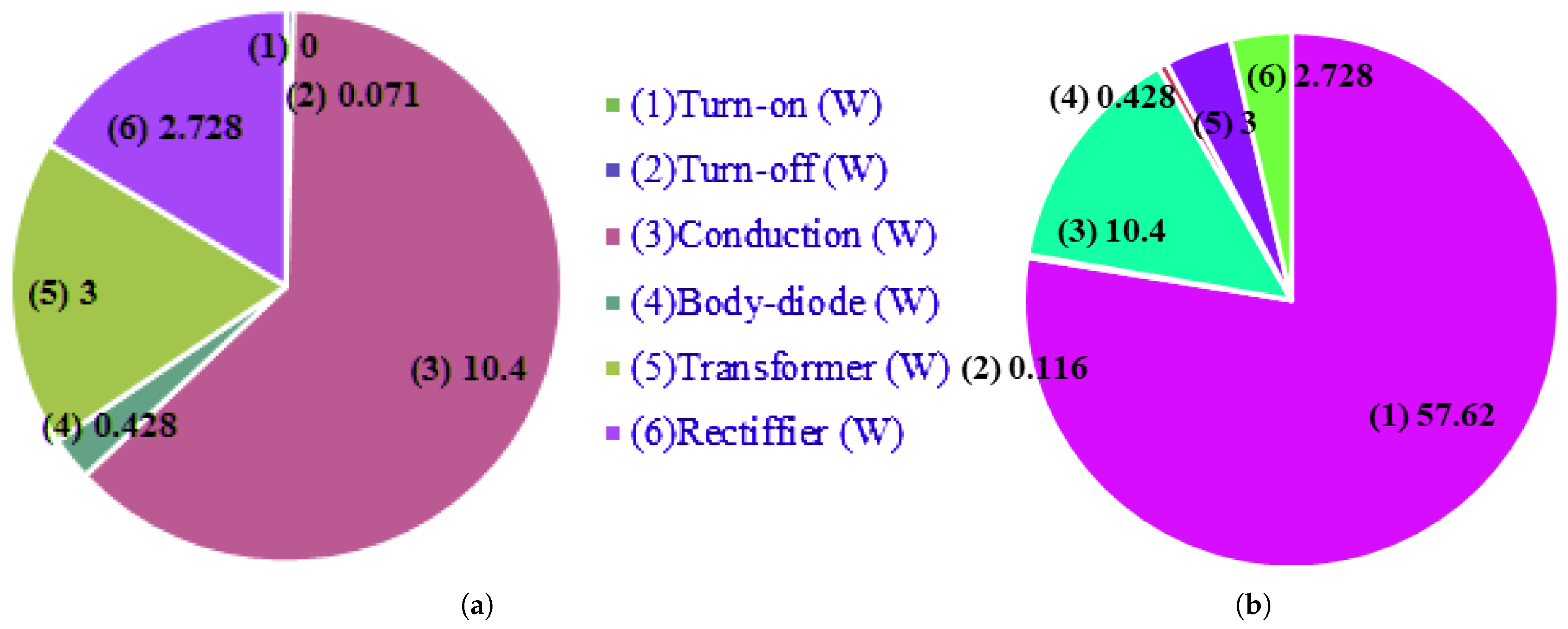
  • Conduct loss calculations for power to determine the efficiency of the converter.
  • Develop an experimental prototype to validate the theoretical and simulation results.
The structure of this paper is organized as follows: Section 2 provides a comprehensive explanation of the LCL-T converter’s operation, utilizing a fixed-frequency PSG control method. In Section 3, a detailed steady-state investigation of the converter is presented using the Fourier series. The design procedure, consisting of a step-by-step guide, is discussed in Section 4. The efficiency of the converter is evaluated through simulations and power loss calculations in Section 5. In Section 6, the converter’s performance is validated experimentally, and the results are compared with the simulation results. Finally, in Section 7, conclusions are drawn from the research findings.

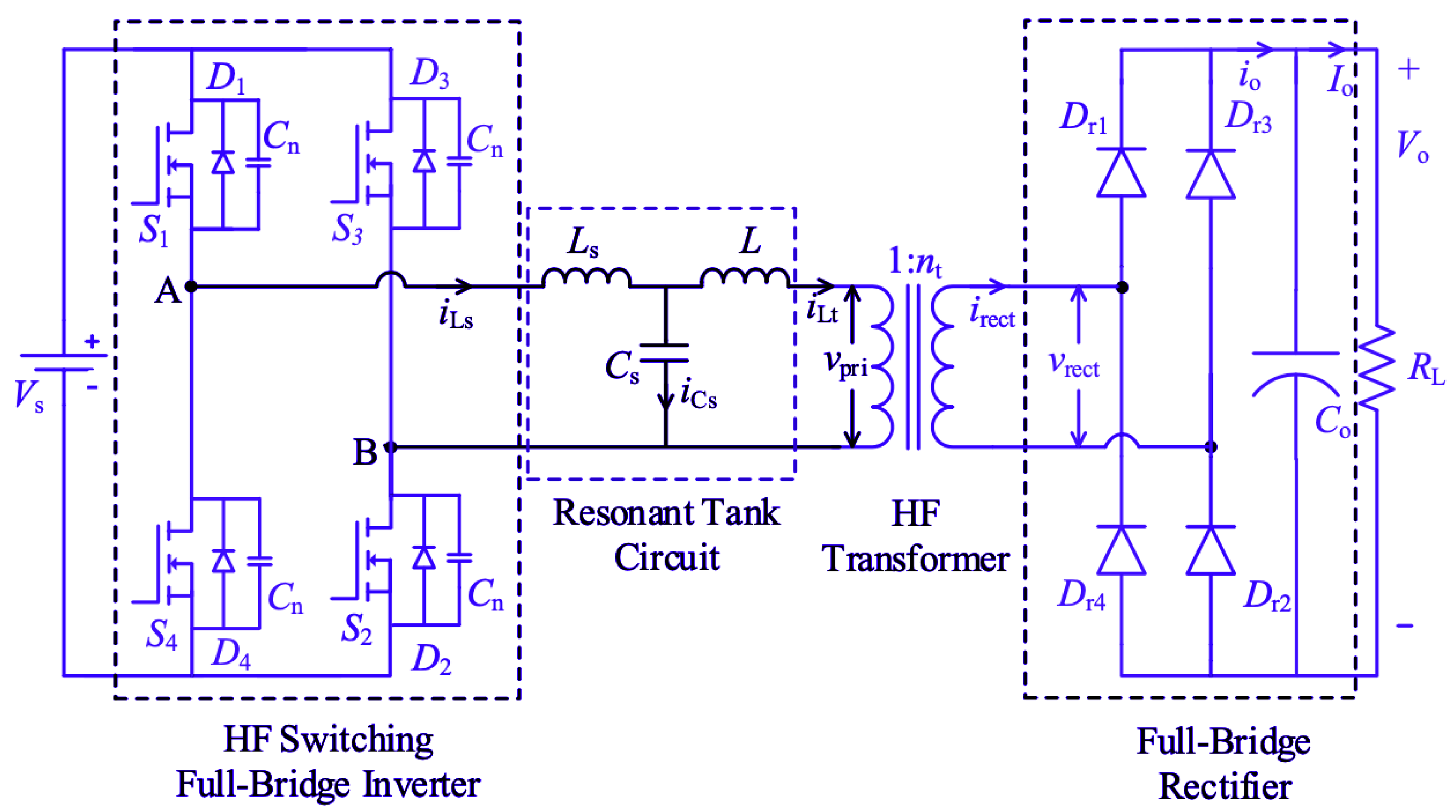
2. Power Circuit and Operations

Figure 2 shows LCL-T type converter. A fixed-frequency phase-shifted gating (PSG) control method is employed to maintain the DC output voltage ( V o ) constant against voltage at input ( V s ), and load ( R L ) fluctuations. To ensure the switches of the high-frequency operated inverter operate with zero voltage switching (ZVS), the converter is operated in the mode where the power factor (pf) is lagging. The typical operating waveforms of the LCL-T converter controlled with a PSG scheme and operating in lagging pf mode are given in Figure 3. To maintain a constant V o , the inverter voltage ( v A B ) at the output-side pulse width ( δ ) is adjusted, with the deviation in δ (i.e., π α ) dependent on the phase-shift angle ( α ) between the gating signals of the inverter switches ( v G S 1 v G S 4 ), as per the control scheme depicted in Figure 3. The control scheme for the phase-shifted gating involves shifting the gating signals of the switches in the lagging leg, namely, S 2 and S 3 , with respect to the gating signals of the switches in the leading leg, namely, S 1 and S 4 , as illustrated in Figure 3. This shift in the gating signals enables the determination of the angle α .

3. Steady-State Analysis Using Fourier series

A Fourier-series (FS)-based method [35] is employed to analyze the steady-steady behavior of the LCL-T resonant converter. This approach considers n-harmonic components of voltages and current waveforms unlike the fundamental harmonic approximation (FHA) method [32,33]. This makes the performance prediction of the converter at reduced load more accurate and provides more efficient results than the FHA analysis method.

3.1. Converter Modelling

After changing the transformer with its T-equivalent circuit, the converter circuit of Figure 2 is redrawn in Figure 4a to establish a connection with the output terminals of the inverter (A, B); the primary side of the HF transformer is interconnected. To simplify the circuit analysis, the magnetizing inductance ( L m ) is treated as an open circuit since it draws negligible current due to its large value. Then, the series combination of L, L 1 , and L 2 is reduced to a single inductance L t L 2 = L 1 + L , as depicted in Figure 4b. The voltage source v r e c t is introduced to represent the diode rectifier, filter capacitor, and load in a simplified manner in Figure 4b. In Figure 4c, the phasor circuit diagram for the nth harmonic is presented to aid in the analysis.

3.2. Normalization

A superscript (’) is used to denote the parameters that are referred to HF transformer’s primary side. To simplify the analysis, all quantities are normalized. The chosen bases are as follows:
V B = V s ( m i n ) , Z B = L s C s , I B = V B Z B
V s ( m i n . ) is minimum input voltage; impedance and current base are Z B are I B , respectively. The subscript ‘n’ and ‘0’, respectively, denote the nth harmonic and normalized quantities. To normalize the reactive elements of the nth harmonic shown in Figure 4c, the following unique expression is used:
X L s n = n ω s L s 1 , X L s n 0 = n F 1 X C s n = C s 1 / ( ω s n ) , X C s n 0 = F 1 / n X L t n = n ω s L t 1 , X L t n 0 = n K / F 1 F = f s f r 1 ; K = L t L s 1
where f s = frequency of switching and f r = frequency of resonant in Hz.
The converter voltage gain is obtained as:
M = V o / V s = V o / ( n t V s )
where V o is the primary referred output voltage and n t is transformer turns ratio.
The normalized value of the load current is obtained as:
J = I o / I B = ( n t I o ) / I B

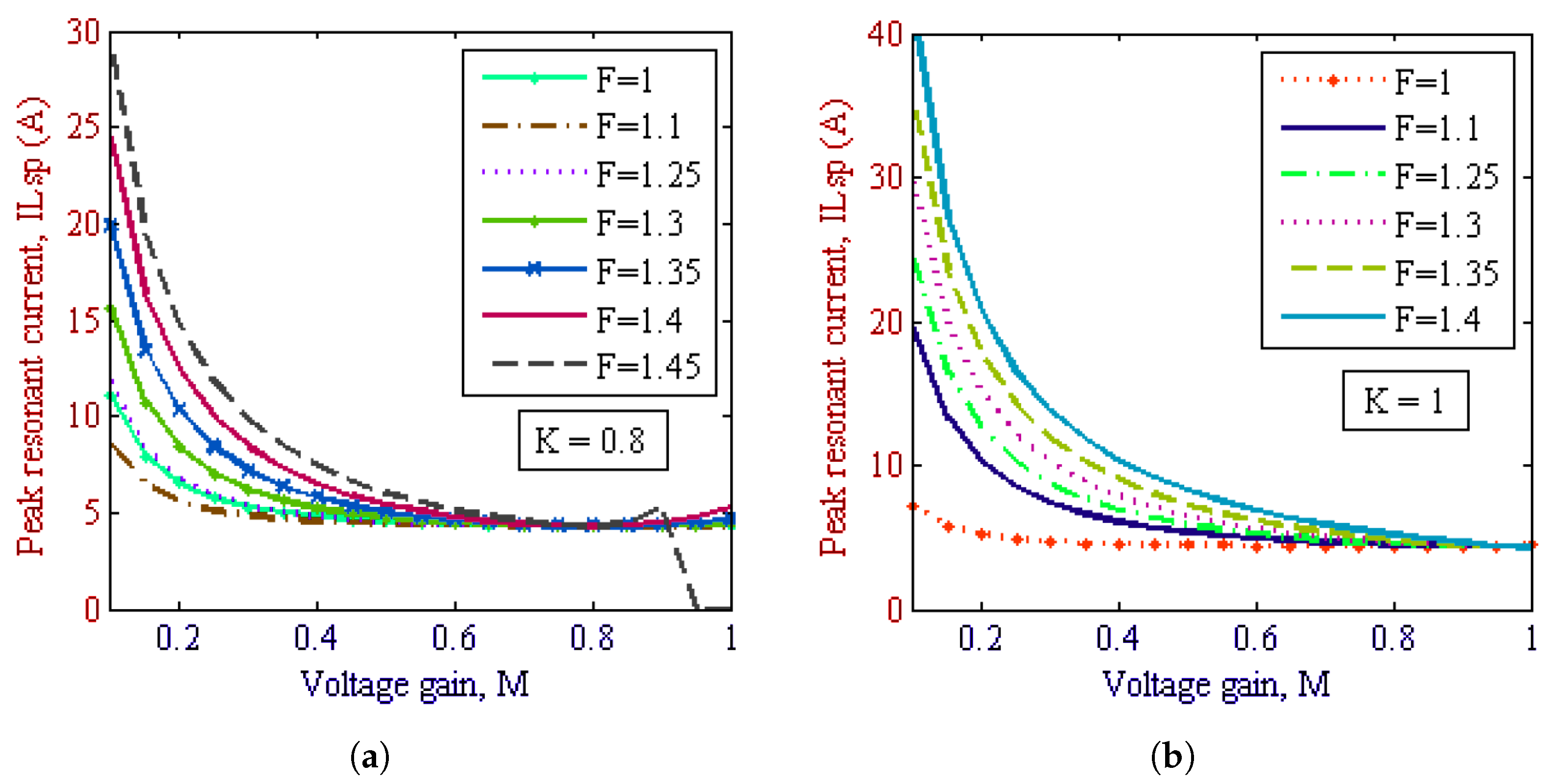
3.3. Investigation of the Converter

From Figure 3, the inverter output voltage v A B and rectifier input voltage v r e c t in the time domain are derived as:
v A B ( t ) = n = 1 , 3 , 5 . . . 4 V s n π Sin n δ 2 Sin ( n ω s t )
v r e c t ( t ) = n = 1 , 3 , 5 . . . 4 V o n π Sin ( n ω s t n θ )
The normalized value of v A B and v r e c t can be obtained as:
v A B 0 ( t ) = n = 1 , 3 , 5 . . . 4 n π Sin n δ 2 Sin ( n ω s t )
v r e c t 0 ( t ) = n = 1 , 3 , 5 . . . 4 M n π Sin ( n ω s t n θ )
The pulse width angle δ of v A B and θ (phase shift) of v r e c t with respect to v A B (as shown in Figure 3) are related by the equation. Referring to Figure 4c, the currents are normalized and simplified as:
i L s 0 ( t ) = n = 1 , 3 , 5 . . . 4 n π 1 Z n 0 [ M X C s n 0 . Cos ( n ω s t n θ ) ( X L t n 0 + X C s n 0 ) Sin n δ 2 Cos ( n ω s t ) ]
i L t 0 ( t ) = n = 1 , 3 , 5 . . . 4 n π 1 Z n 0 [ X C s n 0 Sin n δ 2 Cos ( n ω s t ) M ( X L s n 0 + X C s n 0 ) . Cos ( n ω s t n θ ) ]
where
Z n 0 = X L s n 0 X L t n 0 + X C s n 0 ( X L s n 0 + X L t n 0 )
The normalized voltage across C s is obtained as follows: v C s 0 ( t ) = ( i L s 0 ( t ) i L t 0 ( t ) ) . j X C s n 0
v C s 0 ( t ) = n = 1 , 3 , 5 . . . 4 n π X C s n 0 Z n 0 M X L s n 0 . Sin ( n ω s t n θ ) + X L t n 0 Sin n δ 2 Sin ( n ω s t )
The normalized resonant inductor current i L s 0 is:
i L s 0 ( t ) = n = 1 , 3 , 5 . . . i L s n 0 p . Sin ( n ω s t ϕ )
where
i L s n 0 p = ( i L s n 0 p 1 2 + i L s n 0 p 2 2 )
i L s n o p 1 = 4 n π 1 Z n 0 M X C s n 0 . Cos ( n θ ) Sin n δ 2 ( X L t n 0 + X C s n 0 )
i L s n 0 p 2 = 4 n π 1 Z n 0 M X C s n 0 Sin ( n θ )
ϕ = tan 1 i L s n o p 1 / i L s n o p 2
The normalized total external inductor current i L t 0 in time domain is as
i L t 0 ( t ) = n = 1 , 3 , 5 . . . i L t n 0 p . Sin ( n ω s t + γ 1 )
where
i L t n 0 p = ( i L t n 0 p 1 2 + i L t n 0 p 2 2 )
i L t n 0 p 1 = 4 n π 1 Z n 0 M ( X L s n 0 + X C s n 0 ) Cos ( n θ ) X C s n 0 Sin n δ 2
i L t n 0 p 2 = 4 n π 1 Z n 0 M ( X L s n 0 + X C s n 0 ) Sin ( n θ ) ;
γ 1 = tan 1 i L t n o p 1 / i L t n o p 2
The normalized resonant capacitor voltage v C s 0 in time domain is as:
v C s 0 ( t ) = n = 1 , 3 , 5 . . . v C s n 0 p . Sin ( n ω s t + γ 2 )
where
v C s n 0 p = ( v C s n 0 p 1 2 + v C s n 0 p 2 2 )
v C s n 0 p 1 = 4 n π X C s n 0 Z n 0 M X L s n 0 Cos ( n θ ) + Sin n δ 2 X L t n 0
v C s n 0 p 2 = 4 n π X C s n 0 Z n 0 M X L s n 0 Sin ( n θ )
γ 2 = tan 1 v C s n o p 1 / v C s n o p 2
The effective values of the currents flowing through the inductors i L s and i L t and the voltage across the capacitor v C s can be expressed as:
I L s 0 r = n = 1 , 3 , 5 . . . i L s n 0 p 2 · 1 2
I L t 0 r = n = 1 , 3 , 5 . . . i L t n 0 p 2 · 1 2
v C s 0 r ( t ) = n = 1 , 3 , 5 . . . v C s n 0 p 2 · 1 2
To obtain the normalized value J of the load current I o , which is the average value of i o , the expression for i o given in (10) is considered for 0 ω s t π . Here, i o is equal to i L t .
J = n = 1 , 3 , 5 . . . 8 n 2 π 2 Z n X C s n Sin n δ 2 Sin ( n θ )
The initial value of ‘ θ ’ is required to solve (5) to (18). This can be carried out by solving (10). The phase angle between the v r e c t and i r e c t (i.e., i L t ) is zero. Therefore, i L t = 0 at ω s t = θ . Therefore,
0 = n = 1 , 3 , 5 . . . 4 n π 1 Z n 0 M ( X L s n 0 + X C s n 0 ) X C s n 0 ) . Sin n δ 2 Cos ( n θ )
The initial value of θ (i.e., θ 1 ) is determined by solving (19) at n = 1 . Therefore,
Cos ( θ 1 ) = M X C s 10 + X L s 10 X C s 10 Sin n δ 2
The ratio of the kVA and kW rating of the circuit is:
k V A k W = I L s 0 r 2 X L s n 0 + I C s 0 r 2 X C s n 0 + I L t 0 r 2 X L t n 0 P o
where P o = rated output power. The components L s and C s can be determined using (1) and (2) as follows:
L s = Z B ω r = M J V B 2 F 2 π f s P o , C s = 1 Z B ω r = P o F 2 π f s M J V B 2
The value of L t can be obtained as L t = K L s .

4. Design Consideration

Table 1 presents the key parameters for the designed converter. To achieve an efficient and compact converter design, it is crucial to select appropriate parameters such as frequency ratio, inductor ratio, and DC voltage gain (F, K, and M). To determine appropriate design parameters, one can refer to the design curves presented in Figure 5, Figure 6 and Figure 7, which are generated using the analysis described in Section 3. The harmonic orders beyond 100 have a negligible impact on the voltage and current waveforms; therefore, they are disregarded. Additionally, when F > 1 , the converter is operated with a lagging current.

Design Trade-Offs

Figure 5 shows the variations in kVA/kW of the tank circuit with reference to conversion gain (M). The resonant tank’s kVA/kW rating exhibits the following trends: Firstly, as shown in Figure 5a, decreasing the frequency ratio (F) leads to a decrease in the kVA/kW of the resonant tank, with the effect becoming less drastic for F 1.4 . Secondly, Figure 5b shows that reducing the inductor ratio (K) also decreases the kVA/kW, but this decrement is relatively small for K 0.8 . Finally, Figure 5 demonstrates that the kVA/kW decreases as the voltage gain (M) increases, indicating that M is nearly equal to 1. Additionally, Figure 6 shows the variations in I L s p versus M for different F with fixed K set to 0.8 (Figure 6a) and 1 (Figure 6b). Analyzing Figure 6a, it can be observed that an increase in the frequency ratio (F) and inductor ratio (K) results in an increase in the peak resonant current ( I L s p ). The analysis in Figure 6a reveals that the minimum I L s p occurs at M = 0.8 with K = 0.8 for F = 1.4, in contrast to other F values. The curves of δ versus I o for different F with K set to 0.8 are depicted in Figure 7a, which indicate that the necessary pulse width angle for regulating the output voltage with respect to input and load voltage changes is negligible at F = 1.4 relative to other F values. Based on the findings mentioned above, the optimum design parameters are when K is 0.8, F is 1.4, and M is 0.8. Figure 7b presents the plots of the normalized output current (J) as a function of M for the selected values for K and F. The value of J is 1.75 for the chosen value of M. To calculate the circuit elements required for the selected optimum design with the lower value of V s , the following steps were carried out: First, the output voltage referred to as the HF transformer’s primary side, V o , was calculated as V o = M V s = 88 V using (3). Second, the transformer turns ratio was based on the relation n t :( V o / V o ) = 1:0.4. Using (22), L s = 126.21 µH, C s = 39.33 nF, and L t = 100.92 µH. Third, using Equations (12)–(14), the peak values are I L t p = 5.38 A, I L s p = 4.36 A, and V C s p = 367.7 V. Figure 8 shows the design flowchart for the converter.

5. Simulation Results

The operation of the converter utilizing PSG control was examined through PSIM simulations. The steady-state performance with the PSG control scheme was validated by considering different cases with two different input voltage levels and three loading conditions. These cases are as follows: Case-1, where 110 V is set for the V s (min) and the converter operated with full load; Case-2, where 110 V is set for the V s (min) and the converter operated with half load; Case-3, where 110 V is set for the V s (min) and the converter operated with 10% of full-load; Case-4, where 180 V is set for the V s (max) and the converter operated with full load; Case-5, where 180 V is set for the V s (max) and the converter operated with half-load; and Case-6, where 180 V is set for the V s (max) and the converter operated with 10% of full-load. The gating signals of switches were phase shifted to keep the V o steady at its full-load value, as shown in Figure 3. Figure 9 shows a few waveforms obtained from PSIM simulations.
In Figure 9a,b, the voltage across each switch ( v s 1 , v s 2 , v s 3 , and v s 4 ) and current through respective switches ( i s 1 , i s 2 , i s 3 , and i s 4 ) are shown to confirm ZVS. Validation of the zero-voltage switching (ZVS) technique is confirmed as the voltage across the switch remains at zero just before the current in the positive direction begins to build up for all four switches. This phenomenon holds true for the cases involving the V s (min.), which are denoted as Case-1 to -3. Nevertheless, for these cases of V s (max.) (i.e., Case-4 to -6), two switches lose ZVS (Figure 9b). The inverter voltage v A B , current i L s , voltage across resonant capacitor ( v C s ), transformer primary voltage ( v p r i ), inductor current ( i L t ), rectifier input voltage ( v r e c t ) and current ( i r e c t ) are given in Figure 9c,d. In PSG control, the maximum peak current through the resonant inductor, which is the same as the switch current, is observed at Case-4 ( V s (max.), full load) and the measured value is 4.58 A. In Case-3, which corresponds to V s (min.) and 10% of full load, the inductor experiences the minimum peak current of 3.11 A. To enhance efficiency at lower loads, it is crucial to reduce the peak resonant current as the load decreases. The power loss breakdown for 300 W is shown in Figure 10. The main components used in this theoretical power loss calculation are as follows. MOSFET: IRF740, Diodes: UF5404, HF transformer’s power dissipation is considered to be 1% of the rated power capacity.

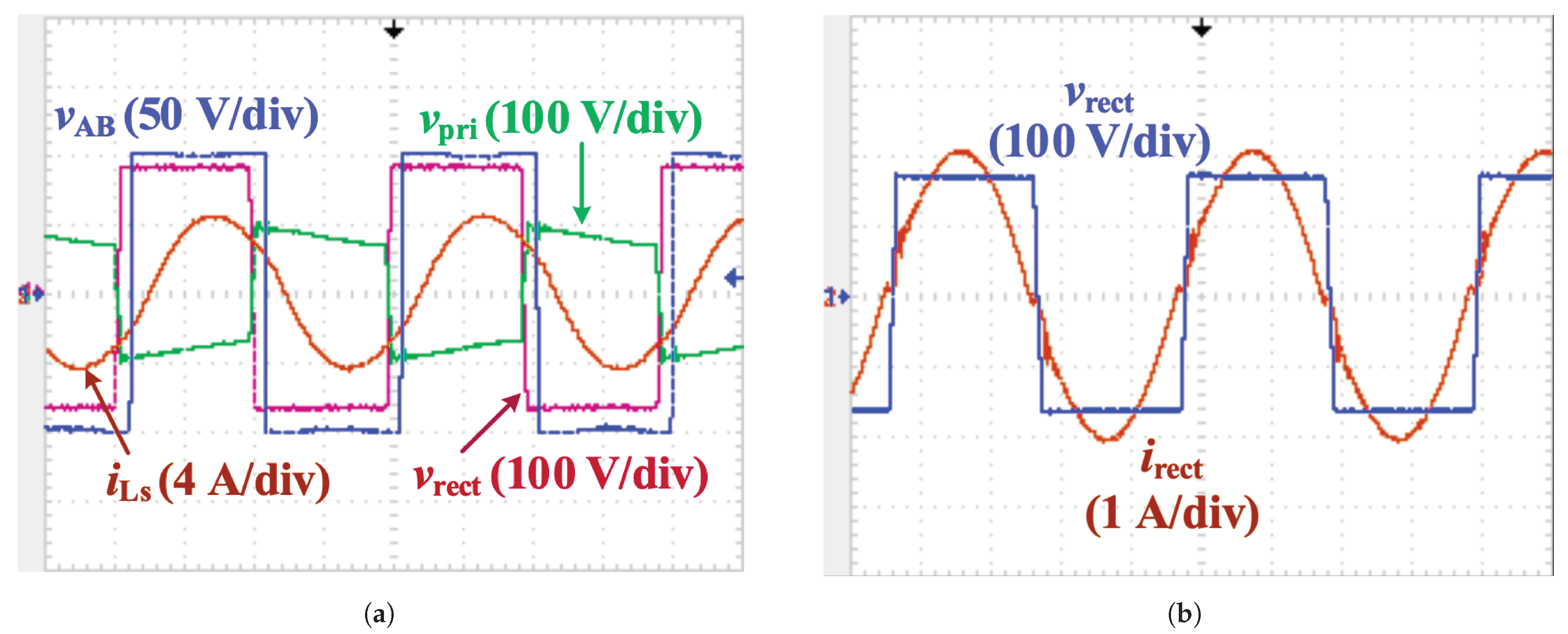
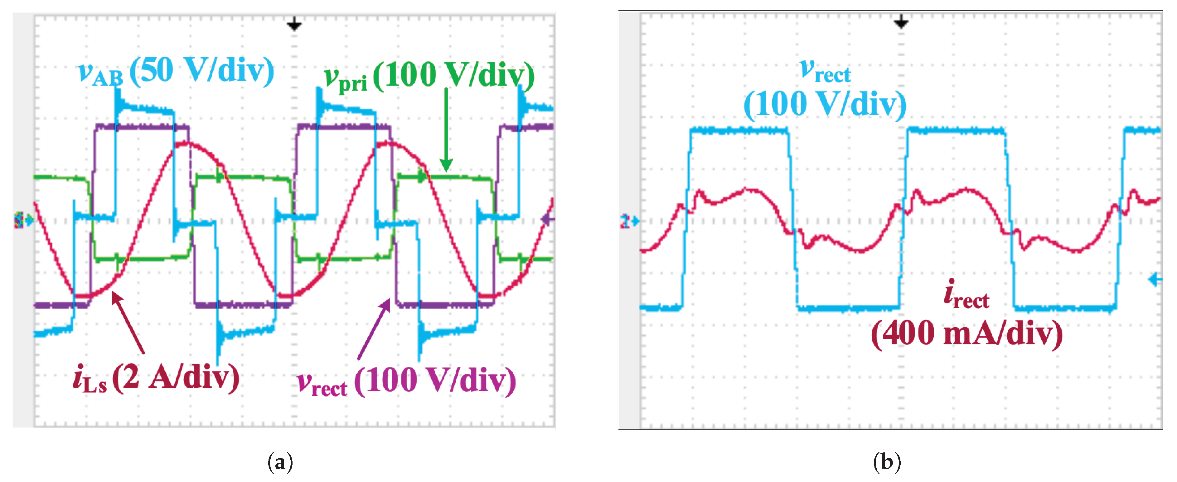
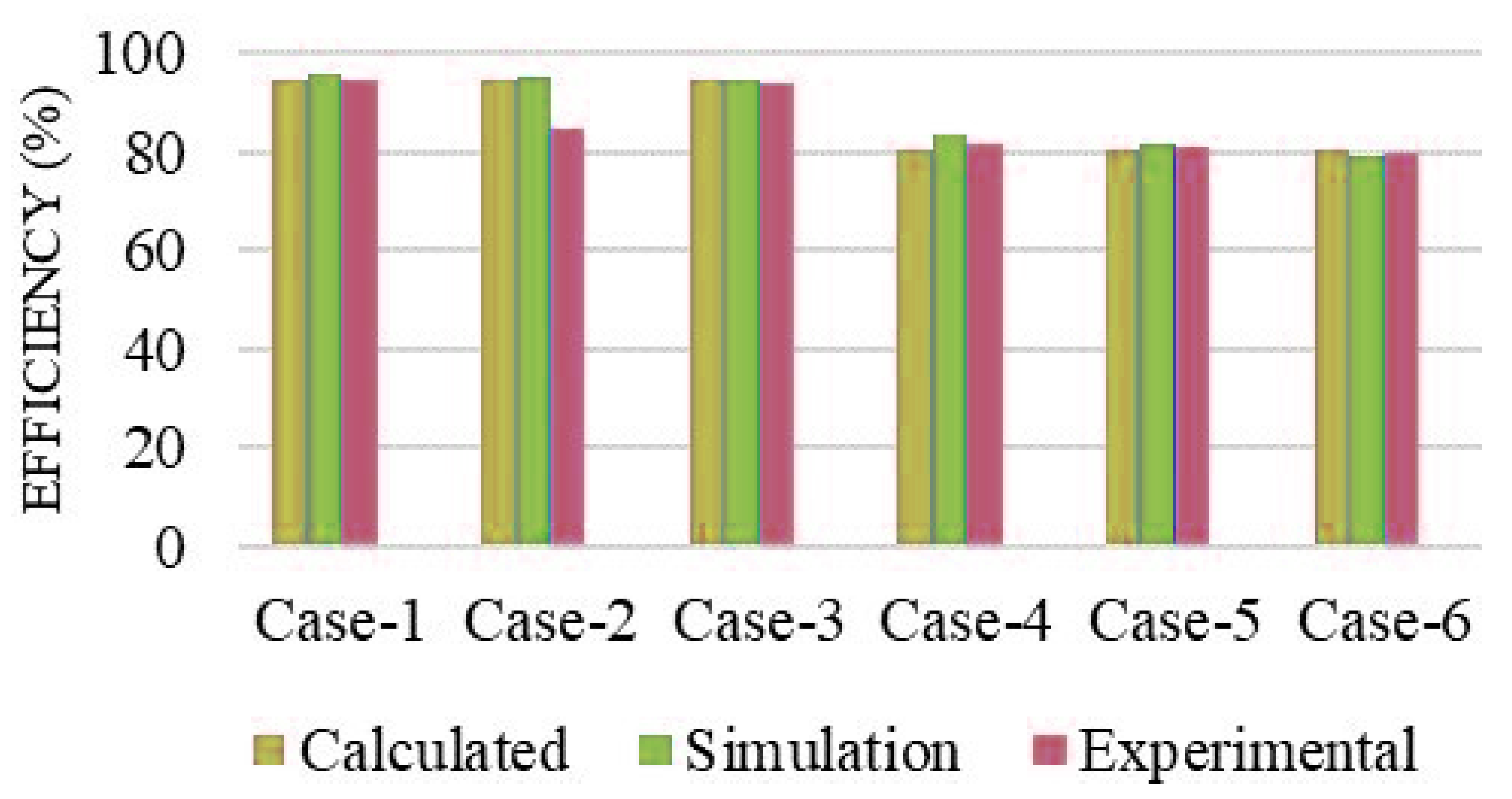
6. Experimental Results

Figure 11 depicts a laboratory-built LCL-T resonant converter with a 300 W experimental setup. Table 2 outlines the components that were used to build the converter circuit. The EE4215 ferrite core and litz wires were used to design the high-frequency transformer. The resonant inductor L s was constructed using 45 turns of 1.56 mm 2 litz wire on a toroidal core. The resonant inductor L s was tested for its inductance value at a frequency of 100 kHz using an LCR meter (GW Instek 6300), and the measured value was found to be 122.81 µH. The total leakage inductance referred to as the primary side was measured to be 3.45 µH. An additional external inductance of 94.8 µH (98.25 µH–3.45 µH) was constructed and connected to the primary side of the transformer, which resulted in a total inductance value of 98.25 µH. The MOSFETs are driven by gating signals, which are generated through the utilization of a Nexys DDR4 artex-7 FPGA board. Recalculation of the switching frequency using (2) results in 103 kHz due to the slightly different built values of the resonant inductor and capacitor. Experimental waveforms of inverter output voltage ( v A B ), resonant inductor current ( i L s ), transformer primary voltage ( v p r i ), and rectifier input voltage ( v r e c t ), rectifier input voltage ( v r e c t ) and current ( i r e c t ) considering different load conditions are presented in Figure 12, Figure 13, Figure 14, Figure 15, Figure 16 and Figure 17. The pulse width of v A B reduces with the change in the load/input voltage for regulating the output voltage. The resonant inductor peak current shows a decreasing trend from 5.07 A at full-load and V s (max.) = 180 V to 3.02 A at 10% of full load and V s (min.) = 110 V. In addition, it is worth noting that the current and voltage waveforms of the diode rectifier exhibit a phase alignment. Hence, power loss is minimum in the diode rectifier. Table 3 contains a comparison of the calculated, simulated, and experimental results. The purpose of the comparison is to evaluate the accuracy of the simulation and calculation results in relation to the experimental data. The change in pulse width is narrow to keep the output voltage constant for variations in the load/input voltage. Therefore, this converter can be used in applications with a wide range of variations in input voltage/load. Efficiency comparison for different cases at calculation, simulation, and experiment is shown in Figure 18. There are various factors that could have led to the differences observed between these outcomes:
(i)
In theoretical calculations, all components such as switches, diodes, inductors, capacitors, and HF transformers are assumed to be ideal. However, in simulations, the R D S resistance in MOSFETs (IRF 740) and a 1V voltage drop in UF5404 are taken into account, while all other elements are still considered ideal. In the prototype, components experience voltage and power losses.
(ii)
The theoretical calculations assumed 1% power loss for the utilized transformer, while in prototype testing, the copper loss changes according to load, and the core losses remain constant.
(iii)
In the practical circuit, a small deviation in component values is inevitable due to the challenges in constructing accurate values of components.
(iv)
The theoretical calculations do not take into account any dead gap whereas, in the experiment, a dead gap of approximately 150 ns is introduced.
The comparison of resonant-power-converter topologies and control schemes is tabulated in Table 4. A comparison between the LCL-T circuit and other resonant circuits can be found in Table 5.

7. Conclusions

Using Fourier-series calculations, the behavior of the fixed-frequency phase-shift regulated LCL-T type converter is investigated. The Fourier-series approach considers n-harmonic components; hence, it gives efficient and accurate results. The theoretical expectations were verified by building a laboratory prototype of the converter. A loss analysis was performed. It is shown that a small change in δ is sufficient to keep the constant voltage at the output for the wide variation in the voltage at the input and the value of the load. In case of low input voltage, all inverter switches turn on with ZVS, and when the input voltage is high, two switches lose ZVS. As a future work, two auxiliary ZVT circuits can be employed for making the non-ZVS switches achieve ZVS so that all the converter switches operate fully with ZVS for any input voltage and load. The calculation and observed simulation and experimental findings are nearly in good agreement. The proposed work goals support a reliable, cost-effective energy system, which is one of the United Nations’ SDG 7 goals. Using a zero voltage switching method, this work promises to make a good energy-efficient system (SDG 12).

Author Contributions

Conceptualization, V.B.R.; methodology, V.B.R.; software, V.B.R. and M.S.B.; validation, V.B.R. and M.S.B.; formal analysis, V.B.R. and M.S.B.; investigation, V.B.R., M.S.B. and U.S.; resources, V.B.R., M.S.B. and U.S.; writing—original draft preparation, V.B.R.; writing—review and editing, M.S.B. and U.S.; visualization, M.S.B. and U.S.; funding acquisition, U.S. and M.S.B. All authors have read and agreed to the published version of the manuscript.

Funding

This work was supported by the research grants (SEED-2022-CE-103) and (SEED-2022-CE-95); Prince Sultan University; Saudi Arabia. The authors would like to acknowledge the support of Prince Sultan University for paying the Article Processing Charges (APC) of this publication.

Data Availability Statement

Not applicable.

Acknowledgments

The authors would like to acknowledge the support of the Renewable Energy Lab (REL) at Prince Sultan University in Saudi Arabia for providing facility support. The authors would like to acknowledge the support of Prince Sultan University for paying the Article Processing Charges (APC) of this publication.

Conflicts of Interest

The authors declare no conflict of interest.

References

  1. Rezvanyvardom, M.; Mirzaei, A.; Heydari, S. Fully Soft-Switching Nonisolated Quasi-Z-Source DC-DC Converter with High-Voltage Gain. IEEE J. Emerg. Sel. Top. Power Electron. 2021, 9, 1854–1862. [Google Scholar] [CrossRef]
  2. Kanamarlapudi, V.R.K.; Wang, B.; Kandasamy, N.K.; So, P.L. A New ZVS Full-Bridge DC–DC Converter for Battery Charging With Reduced Losses Over Full-Load Range. IEEE Trans. Ind. Appl. 2018, 54, 571–579. [Google Scholar] [CrossRef]
  3. Chen, Y.; Xu, D. Review of Soft-Switching Topologies for Single-Phase Photovoltaic Inverters. IEEE Trans. Power Electron. 2022, 37, 1926–1944. [Google Scholar] [CrossRef]
  4. Ahmed, N.A.; Madouh, J.Y. High-frequency full-bridge isolated DC–DC converter for fuel cell power generation systems. Electr. Eng. 2018, 100, 239–251. [Google Scholar] [CrossRef]
  5. Cheng, X.F.; Liu, C.; Wang, D.; Zhang, Y. State-of-the-Art Review on Soft-Switching Technologies for Non-Isolated DC-DC Converters. IEEE Access 2021, 9, 119235–119249. [Google Scholar] [CrossRef]
  6. Jiang, Y.; Wang, L.; Fang, J.; Li, R.; Han, R.; Wang, Y. A High-Efficiency ZVS Wireless Power Transfer System for Electric Vehicle Charging with Variable Angle Phase Shift Control. IEEE J. Emerg. Sel. Top. Power Electron. 2020, 9, 2356–2372. [Google Scholar] [CrossRef]
  7. Wu, X.; Liu, Z.; Du, J.; Yu, B. Research on Zero Voltage Switching Non-inductive Current Circulation Control of Bidirectional DC/DC Converter for Hybrid Energy Source System of Electric Vehicle. J. Electr. Eng. Technol. 2021, 16, 873–887. [Google Scholar] [CrossRef]
  8. Elizondo, D.; Barrios, E.L.; Larequi, I.; Ursua, A.; Sanchis, P. Zero-Loss Switching in LLC Resonant Converters under Discontinuous Conduction Mode: Analysis and Design Methodology. IEEE Trans. Ind. Appl. 2023, 59, 3576–3592. [Google Scholar] [CrossRef]
  9. Kong, J.; Smedley, K.M.; Cheng, H. Full-Range Regulation Method for Half-Bridge Series Resonant Converter. IEEE Trans. Ind. Electron. 2023, 70, 1905–1915. [Google Scholar] [CrossRef]
  10. Hong, J.; Guan, M.; Lin, Z.; Fang, Q.; Wu, W.; Chen, W. Series-Series/Series Compensated Inductive Power Transmission System with Symmetrical Half-Bridge Resonant Converter: Design, Analysis, and Experimental Assessment. Energies 2019, 12, 2268. [Google Scholar] [CrossRef]
  11. Chen, J.; Xu, Y.; Lu, H.; Yan, Z.; Yu, Z.; Li, Q.; Tan, Y. Fixed Frequency LCC Resonant Converter Modeling and Optimal Design for High-Voltage Capacitor Charging Power Supply in Constant Power Control. IEEE Trans. Ind. Appl. 2023; 1–12, early access. [Google Scholar] [CrossRef]
  12. Lee, I.O. Hybrid DC-DC Converter with Phase-Shift or Frequency Modulation for NEV Battery Charger. IEEE Trans. Ind. Electron. 2016, 63, 884–893. [Google Scholar] [CrossRef]
  13. Wei, Y.; Luo, Q.; Woldegiorgis, D.; Mhiesan, H.; Mantooth, A. Characteristics Analysis of LLC and LCL-T Resonant Tank. In Proceedings of the 2020 IEEE Transportation Electrification Conference and Expo, ITEC 2020, Chicago, IL, USA, 23–26 June 2020; pp. 427–432. [Google Scholar] [CrossRef]
  14. Tan, X.; Ruan, X. Equivalence Relations of Resonant Tanks: A New Perspective for Selection and Design of Resonant Converters. IEEE Trans. Ind. Electron. 2016, 63, 2111–2123. [Google Scholar] [CrossRef]
  15. Patarau, T.M.; Petreus, D.M.; Ferencz, I.; Orban, Z. Comparison between LLC and Phase-Shift Converter with Synchronous Rectification for High Power, High Current Applications. In Proceedings of the 2020 IEEE 26th International Symposium for Design and Technology in Electronic Packaging, SIITME 2020, Pitesti, Romania, 21–24 October 2020; pp. 398–403. [Google Scholar] [CrossRef]
  16. Khosrogorji, S.; Soori, S.; Torkaman, H. A new design strategy for DC/DC LLC resonant converter: Concept, modeling, and fabrication. Int. J. Circuit Theory Appl. 2019, 47, 1645–1663. [Google Scholar] [CrossRef]
  17. Tan, H.; Yang, X.; Liu, Y.; Yan, C.; Zheng, T.Q.; Igarashi, S.; Chen, Q. Short-Circuit Protection for Resonant Switched-Capacitor Converter. IEEE Trans. Ind. Appl. 2022, 59, 1956–1968. [Google Scholar] [CrossRef]
  18. Wu, H.; Jin, X.; Hu, H.; Xing, Y. Multielement Resonant Converters With a Notch Filter on Secondary Side. IEEE Trans. Power Electron. 2016, 31, 3999–4004. [Google Scholar] [CrossRef]
  19. Bu, H.; Guan, J.; Zhang, C.; Li, Z. Optimal Control Strategy of CLLC Bidirectional Resonant Converter under Light Load. In Proceedings of the 2022 9th International Forum on Electrical Engineering and Automation, IFEEA 2022, Zhuhai, China, 4–6 November 2022; pp. 921–924. [Google Scholar] [CrossRef]
  20. Fei, C.; Lee, F.C.; Li, Q. Digital Implementation of Soft Start-Up and Short-Circuit Protection for High-Frequency LLC Converters With Optimal Trajectory Control (OTC). IEEE Trans. Power Electron. 2017, 32, 8008–8017. [Google Scholar] [CrossRef]
  21. Hwu, K.I.; Guo, Y.S. Efficiency improvement for LLC converter based on automatic tuning of blanking time. Int. J. Circuit Theory Appl. 2019, 47, 1477–1501. [Google Scholar] [CrossRef]
  22. Hu, J.; Yang, Z.; Cui, S.; Doncker, R.W.D. Closed-Form Asymmetrical Duty-Cycle Control to Extend the Soft-Switching Range of Three-Phase Dual-Active-Bridge Converters. IEEE Trans. Power Electron. 2021, 36, 9609–9622. [Google Scholar] [CrossRef]
  23. Hu, J.; Soltau, N.; Doncker, R.W.D. Asymmetrical duty-cycle control of three-phase dual-active bridge converter for soft-switching range extension. In Proceedings of the ECCE 2016—IEEE Energy Conversion Congress and Exposition, Milwaukee, WI, USA, 18–22 September 2016. [Google Scholar] [CrossRef]
  24. Veeramallu, V.K.; Porpandiselvi, S.; Narasimharaju, B.L. A Nonisolated Wide Input Series Resonant Converter for Automotive LED Lighting System. IEEE Trans. Power Electron. 2021, 36, 5686–5699. [Google Scholar] [CrossRef]
  25. Bai, C.; Han, B.; Kwon, B.H.; Kim, M. Highly Efficient Bidirectional Series-Resonant DC/DC Converter over Wide Range of Battery Voltages. IEEE Trans. Power Electron. 2020, 35, 3636–3650. [Google Scholar] [CrossRef]
  26. Shen, Y.; Wang, H.; Al-Durra, A.; Qin, Z.; Blaabjerg, F. A Bidirectional Resonant DC-DC Converter Suitable for Wide Voltage Gain Range. IEEE Trans. Power Electron. 2018, 33, 2957–2975. [Google Scholar] [CrossRef]
  27. Abbasi, M.; Emamalipour, R.; Cheema, M.A.M.; Lam, J. A Constant-Frequency High-Voltage Gain Resonant Converter Module With Semiactive Phase-Shifted Voltage Multiplier for MVdc Distribution. IEEE J. Emerg. Sel. Top. Power Electron. 2022, 10, 3603–3616. [Google Scholar] [CrossRef]
  28. Ma, X.; Wang, P.; Bi, H.; Wang, Z. A Bidirectional LLCL Resonant DC-DC Converter with Reduced Resonant Tank Currents and Reduced Voltage Stress of the Resonant Capacitor. IEEE Access 2020, 8, 125549–125564. [Google Scholar] [CrossRef]
  29. Xu, J.; Wei, Y.; Cheng, X.; Yang, H.; Xue, H.; Wang, X. Univesal Design of LLC Resonant Converter with Fixed Switching Frequency. In Proceedings of the 2020 IEEE International Conference on Information Technology, Big Data and Artificial Intelligence, ICIBA 2020, Chongqing, China, 6–8 November 2020; pp. 1323–1328. [Google Scholar] [CrossRef]
  30. Vinnikov, D.; Chub, A.; Kosenko, R.; Zakis, J.; Liivik, E. Comparison of Performance of Phase-Shift and Asymmetrical Pulsewidth Modulation Techniques for the Novel Galvanically Isolated Buck–Boost DC–DC Converter for Photovoltaic Applications. IEEE J. Emerg. Sel. Top. Power Electron. 2017, 5, 624–637. [Google Scholar] [CrossRef]
  31. Shakib, S.M.S.I.; Mekhilef, S. A Frequency Adaptive Phase Shift Modulation Control Based LLC Series Resonant Converter for Wide Input Voltage Applications. IEEE Trans. Power Electron. 2017, 32, 8360–8370. [Google Scholar] [CrossRef]
  32. Reddy, G.V.B.; Nagendrappa, H. Fixed frequency control of LCL-T resonant power converter with capacitive output filter. In Proceedings of the 6th International Conference on Computer Applications In Electrical Engineering-Recent Advances (CERA), Roorkee, India, 5–7 October 2017; pp. 568–573. [Google Scholar] [CrossRef]
  33. Harischandrappa, N.; Bhat, A.K.S. A Fixed-Frequency LCL-Type Series Resonant Converter With a Capacitive Output Filter Using a Modified Gating Scheme. IEEE Trans. Ind. Appl. 2014, 50, 4056–4064. [Google Scholar] [CrossRef]
  34. Reddy G., V.B.; Nagendrappa, H. Modified Gating Signal Controlled High-Frequency Transformer Isolated LCL-T Type DC-DC Resonant Power Converter. In Proceedings of the 2018 8th IEEE India International Conference on Power Electronics (IICPE), Jaipur, India, 13–15 December 2018; pp. 1–6. [Google Scholar] [CrossRef]
  35. Chen, H.; Bhat, A.K.S. A bidirectional dual-bridge LCL-type series resonant converter controlled with modified gating scheme. In Proceedings of the IEEE 8th International Power Electronics and Motion Control Conference (IPEMC-ECCE Asia), Hefei, China, 22–26 May 2016; pp. 3036–3042. [Google Scholar] [CrossRef]
Figure 1. Grid integration of DC renewable energy source—block diagram.
Energies 16 06012 g001
Figure 2. LCL-T-type converter with HF transformer (A and B are nodes in the circuit).
Energies 16 06012 g002
Figure 3. A control scheme waveform for lagging—power—factor mode utilizing fixed—frequency PSG.
Energies 16 06012 g003
Figure 4. Equivalent circuit: (a) T-type circuit illustrating the high-frequency (HF) transformer, (b) with voltage source v r e c t , and (c) harmonic phasor equivalent (nth).
Energies 16 06012 g004
Figure 5. Plots of kVA/kW versus gain (M): (a) K = 0.8, various values of F, (b) F = 1.4, various values of K.
Energies 16 06012 g005
Figure 6. Peak ( I L s p ) resonant current versus gain (M) for different values of F with inductor ratio (a) K set to 0.8, and (b) K set to 1.
Energies 16 06012 g006
Figure 7. Plots (a) δ versus load current, and (b) J versus M with K set to 0.8.
Energies 16 06012 g007
Figure 8. Flowchart of the design procedure.
Energies 16 06012 g008
Figure 9. Simulation waveforms: inverter switch voltages and currents to show ZVS (a) Case-1, (b) Case-4; v A B , i L s , v C s , v p r i , i L t , v r e c t , i r e c t waveforms in (c) Case-1, (d) Case-5.
Energies 16 06012 g009
Figure 10. Power loss calculations at full load ( R L = 161.17   Ω ) with: (a) V s (min.) = 110 V, (b) V s (max.) = 180 V.
Energies 16 06012 g010
Figure 11. Block diagram for experimental setup of LCL-T converter.
Energies 16 06012 g011
Figure 12. Practical results for the minimum voltage and full-load conditions (a) v r e c t , v A B , v p r i , i L s ; (b) i r e c t , v r e c t . The time scale was set to 2.5 µs/div.
Energies 16 06012 g012
Figure 13. Practical results for the minimum voltage and half-load conditions (a) v r e c t , v A B , v p r i , i L s ; (b) i r e c t , v r e c t . The time scale was set to 2.5 µs/div.
Energies 16 06012 g013
Figure 14. Practical results for the minimum voltage and 10%-loading conditions (a) v r e c t , v A B , v p r i , i L s ; (b) i r e c t , v r e c t . The time scale was set to 2.5 µs/div.
Energies 16 06012 g014
Figure 15. Practical results for the maximum voltage and full-load conditions (a) v r e c t , v A B , v p r i , i L s ; (b) i r e c t , v r e c t . The time scale was set to 2.5 µs/div.
Energies 16 06012 g015
Figure 16. Practical results for the maximum voltage and half-load conditions (a) v r e c t , v A B , v p r i , i L s ; (b) i r e c t , v r e c t . The time scale was set to 2.5 µs/div.
Energies 16 06012 g016
Figure 17. Practical results for the maximum voltage and 10%-loading conditions (a) v r e c t , v A B , v p r i , i L s ; (b) i r e c t , v r e c t . The time scale is set to 2.5 µs/div.
Energies 16 06012 g017
Figure 18. Comparision of calculated, simulation and experimental efficiency.
Energies 16 06012 g018
Table 1. Converter parameters.
IndicatorsValue
V s (min.), V s (max.)110.00 V, 180.00 V
V o , P o 220.00 V, 300.00 W
f s 100.00 kHz
Table 2. Components used in the experiment.
ComponentDetails
MOSFET switches ( S 1 S 4 )IRF740 (400 V, 10 A)
L s , L t , C o , C s 122.83 µH, 94.6 µH, 470 µF (400 V), 38.15 nF
HF transformer, turns ratioCore: EE4215, 16:40
D r 1 to D r 4 UF5404 (voltage = 400 V, current = 3 A)
Table 3. Comparison of results.
ParametersCalculationSimulationExperimental
V o (V)220214.62206
I o (A)1.361.331.31
δ (o)180180176.3
I L s r (A)3.042.993.04
I L t r (A)3.803.703.425
V C s r (V)260253254
I i n (A)2.722.7032.6
η (%)94.749694.35
Table 4. Comparison of control schemes for resonant-power-converter topologies.
ParameterADC ControlPhase-Shift ControlModified Gating Control
Switch utilizationUnderutilizedWell utilizedWell utilized
DC blocking capacitor for full-bridge operationRequiredNot requiredNot required
Possibilities of transformer core saturationMaximalMinimalMinimal
Range of duty cycleBroadLimitedVery Limited
Loss of ZVS with maximum input voltageTwo switchesTwo switches1 switch
Table 5. Comparative study of resonant circuit.
CircuitsFactors
Pulse Width Angle ( δ ) ChangeComponent StressesProtection for Short-Circuit LoadSoft-Switching


SRC
Energies 16 06012 i001

Broad


Minimal


Absent


ZVS


PRC
Energies 16 06012 i002

Broad


Maximal


Present


ZVS


LCC
Energies 16 06012 i003

Limited


Maximal


Absent


ZVS


LCL
Energies 16 06012 i004

Moderate


Minimal


Absent


ZVS, ZCS


LCL-T
Energies 16 06012 i005

Limited


Minimal


Present


ZVS
Disclaimer/Publisher’s Note: The statements, opinions and data contained in all publications are solely those of the individual author(s) and contributor(s) and not of MDPI and/or the editor(s). MDPI and/or the editor(s) disclaim responsibility for any injury to people or property resulting from any ideas, methods, instructions or products referred to in the content.

