1. Introduction
Due to their remarkable performance, Phase-Shifted Full-Bridge Converters (PSFBCs) have garnered widespread adoption in medium- and high-power applications, including telecommunications, data centers, and renewable energy systems. PSFBCs employ a full-bridge topology, complemented by a transformer and resonance inductor, to facilitate energy transfer from the input terminal to the output terminal. Zero-Voltage Switching (ZVS) is a prevalent technique employed in PSFBCs to minimize switching loss and enhance conversion efficiency. In a PSFBC, achieving ZVS entails delaying the turn-on of the power switches until the voltage across them reaches zero, which is accomplished by adjusting the phase-shifted angle and dead time between the paired switches. When the upper paired switch is turned off, its voltage rises. By delaying the turn-on of the lower paired switch until the voltage across it reaches zero, ZVS is effectively achieved. The same principle applies when the lower paired switch is turned off, and the upper paired switch is turned on. ZVS is pivotal in PSFBCs as it enables high conversion efficiency and reduces heat dissipation, particularly in medium-and high-power applications [
1,
2,
3,
4]. Hardware reinforcement and the precise control of switch timings are crucial for achieving ZVS, and the PSFBC design must be optimized accordingly.
Several papers have explored performance enhancements of PSFBCs through hardware topologies and control strategies [
5,
6,
7,
8,
9,
10,
11,
12,
13,
14,
15]. Regarding hardware reinforcements, Ref. [
5] introduced an auxiliary circuit to improve ZVS and Zero-Current Switching (ZCS) in conventional PSFBCs, enhancing conversion efficiency and reducing output current ripple. Ref. [
6] proposed a PSFBC configuration consisting of a clamping circuit with two power switches and two diodes, enabling ZVS and ZCS capabilities. Additionally, a resetting transformer ensured ZCS for the lagging-leg switches across a wide load range. Ref. [
7] utilized a center-tapped clamp circuit comprising two diodes and one capacitor in a PSFBC to achieve higher conversion efficiency. This clamp circuit limited the secondary voltage stress to the secondary-reflected input voltage, reducing conduction losses in the secondary rectifier. Ref. [
8] exploited the advantages of input-series–output-parallel PSFBCs to achieve ZVS and ZCS while minimizing duty-cycle and conduction losses through the interaction of two PSFBCs. In [
9], a triple-phase-shift modulation scheme was proposed for the diode-clamped isolated three-level full-bridge DC/DC converter to alleviate transformer voltage stress. While these topology enhancements effectively improve conversion efficiency and reduce component stress in PSFBCs, they often incur additional costs and increase circuit volume [
5,
6,
7,
8,
9]. From the perspectives of control strategy enhancement, Ref. [
10] introduced an asymmetrical PWM approach for a PSFBC with split capacitors and an improved rectifier stage, enabling ZVS and a reduced circulating current. Model predictive control, as presented in [
11], improved the dynamic characteristics of a PSFBC by predicting the next output power and calculating the optimal phase shift based on the model predictive control from output power variations. In [
12], a control scheme adjusting the phase-shift angle and duty ratio during the pre-charge and co-charge stages was proposed to enhance the conversion efficiency of bidirectional PSFBCs. Ref. [
13] explored PWM switching modes for PSFBCs under light-load and standby conditions to improve conversion efficiency and conducted loss analysis. To enhance conversion efficiencies at light loads, [
14] proposed a three-stage dead-time adjustment strategy tailored to load conditions for the power switches of PSFBCs. Ref. [
15] introduced dynamic dead-time control to enhance light-load conversion efficiency in an interleaved PSFBC used in server power applications. Control strategy adjustments offer the advantage of achieving higher stability and improved conversion efficiency without requiring additional components, although they may have certain control limitations [
10,
11,
12,
13,
14,
15].
The performance of a PSFBC is greatly influenced by its magnetic components, namely the transformer and resonance inductor. These components, such as the leakage inductor of the transformer and the resonant inductor, are often utilized to achieve a more substantial ZVS interval. Reducing the resonant inductor value can lead to ZVS failure under light loads, while increasing it can help minimize switching loss but at the expense of higher commutation and circulation losses under medium and heavy loads. Additionally, the transformer turns ratio is crucial in determining the voltage range, effective interval, and magnitude of the primary-side current. Poor design of the transformer turns ratio can result in a larger circulation interval and increased losses. Furthermore, adjustments to the transformer turns ratio and resonant inductor value in a PSFBC can affect its overall conversion efficiency and performance in various application scenarios. Few papers have delved into the effects of these magnetic components on ZVS and conversion efficiency in PSFBCs [
16,
17,
18,
19]. Ref. [
16] derived equations for calculating the necessary resonant inductor value to achieve ZVS, taking into account dead time and magnetizing inductor effects. Ref. [
17] developed an optimization procedure for an integrated transformer employed in a center-tap PSFBC, where the transformer was wound on magnetic legs to reduce conduction losses caused by the alternating-current resistor. The study in [
18] investigated an analytical treatment of ZVS and the interdependence of circuit parameters in PSFBCs. This research provided practical guidelines for tuning ZVS. Ref. [
19] proposed a design for the resonant inductance to enhance conversion efficiency in PSFBCs operating in various application scenarios.
Even when the other circuit components remain unchanged, adjusting the transform turns ratio and resonant inductor value of a PSFBC will affect its overall conversion efficiency and performance. Designing the magnetic components’ parameters of a PSFBC, such as the transformer turns ratio and resonance inductor value, is complicated due to the numerous possible parameter adjustments and combinations. Traditional simulation methods [
13,
14], while offering a certain level of accuracy, do not take into account the impact of circuit parameters. On the other hand, circuit design methods become impractical due to the excessive number of experiments required [
16,
17,
18,
19]. A digital twin of a PSFBC serves as a virtual representation of the physical circuit, allowing for straightforward adjustment and replacement of circuit components and parameters without additional effort. Developing a highly accurate digital twin for a PSFBC can facilitate efficient parameter design through simulations. A digital twin of PSFBCs enabling a more precise loss estimation is proposed in this paper to achieve this objective. By leveraging the digital twin, the optimal combination of transformer turns ratio and resonance inductor value that minimize the operational loss of the PSFBC for a specific application scenario from the possible combinations can be selected. The grid search is used in this paper. The experimental results show the influences of transformer turns ratio and resonant inductor value on the PSFBC and validate the proposed digital twin. The proposed parameter optimization of magnetic components is further evaluated across two application scenarios with varying utilization rates. The simulation results indicate a reduction of approximately 14% in operational loss per hour after applying the parameter optimization of magnetic components for the PSFBC used as a battery charger.
2. Effects of Magnetic Components on PSFBCs
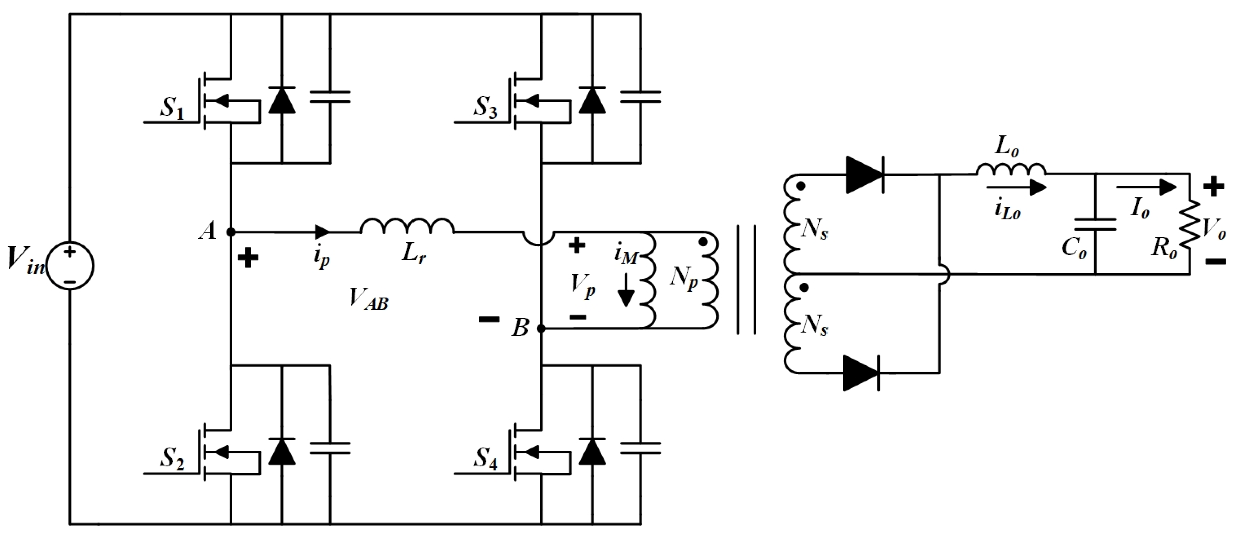
Figure 1 shows the circuit topology of a conventional center-tapped PSFBC where
Vin and
Vo represent the input and output voltages, respectively;
Io is the output current;
Vp and
ip denote the transformer voltage and current at the primary side, respectively;
iM is the exciting current of the transformer;
Vs is the transformer voltage at the secondary side;
S1 to
S4 are the power switches of the full-bridge configuration;
Lr is the resonance inductor,
Np and
Ns correspond to the transformer turns of primary and secondary sides, respectively;
Lo and
Co are the output inductor and capacitor, respectively; and
iLo is the current of
Lo.
Figure 2 indicates the theoretic waveforms of the PSFBC where
Vgs1 to
Vgs4 represent the gate drive signals for power switches
S1 to
S4, respectively;
i1 to
i6 denote the currents at
t1 to
t6, respectively;
Dph,
Dts, and
Deff correspond to the duty ratios of phase-shift switches, transition, and energy transfer regions, respectively. By controlling the phase shifts of
Vgs1 to
Vgs4, ten operating stages, as shown in
Figure 2, can be determined in one switching period. Due to the symmetry, a thorough analysis of the PSFBC requires analyzing five operational stages. The time intervals between
t1 and
t2, between
t2 and
t3, between
t3 and
t4, between
t4 and
t5, and between
t5 and
t6 are the energy transfer region, the resonant region of leading-leg switches, the circulation region, the resonant region of lagging-leg switches, and the transition region, respectively. The duty ratio of the circulation region in
Figure 2 is denoted as
Dcir. The time intervals between
t2 and
t3 and between
t4 and
t5 represent the dead-time intervals for the leading-leg and lagging-leg switches, respectively. The time interval between
t2 and
t5 is typically defined as the current circulating region. A comprehensive analysis of the operating stages can be found in [
13,
14] and will not be further discussed here due to space limitations.
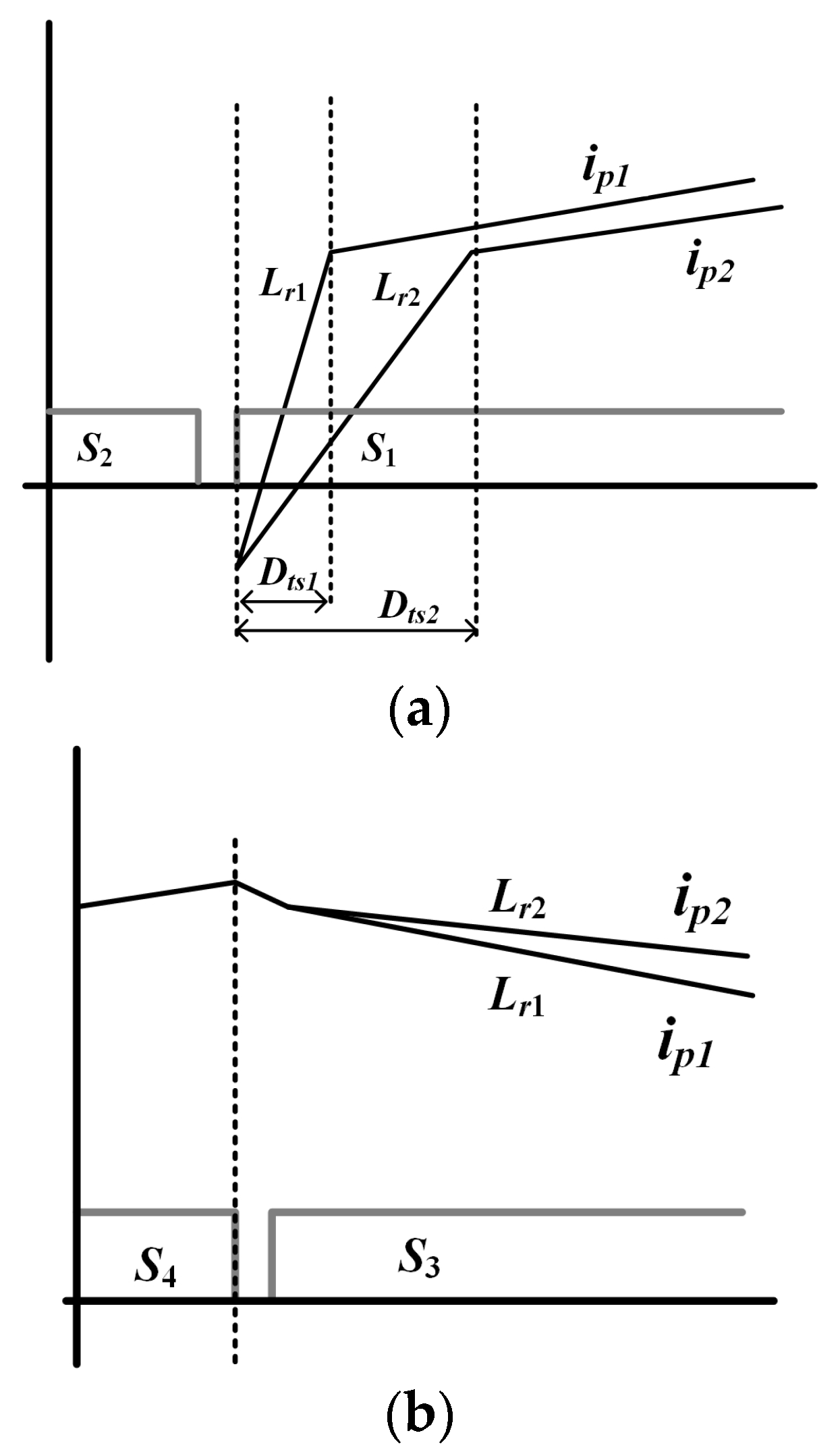
Figure 3 depicts the effects of two distinct resonance inductor values on the primary-side current (
ip) of a PSFBC, with
Lr2 being larger than
Lr1. In
Figure 3,
ip1 and
ip2 are the primary-side currents for
Lr1 and
Lr2, respectively, and
Dts1 and
Dts2 are the time intervals of the transition region for
Lr1 and
Lr2, respectively. Due to the increased inductor value of
Lr2,
Figure 3a illustrates a slower current rise in the transition region, leading to a longer time interval for the transition region and a shorter time interval for the energy transfer region than the smaller inductor value of
Lr1. Furthermore,
Figure 3b demonstrates that the larger inductor value of
Lr2 causes a gradual decline in the current during the circulating region, resulting in a higher Root-Mean-Square (RMS) current in the circulating region compared to the smaller inductor value of
Lr1. Essentially, a larger resonance inductor value can help facilitate ZVS and reduce switching loss. However, it also leads to an increased RMS current in the circulating region, resulting in higher conduction loss. Consequently, a larger resonance inductor value amplifies conduction loss while reducing switching loss. In PSFBCs, switching loss dominates at light loads, whereas conduction loss dominates at heavy loads.
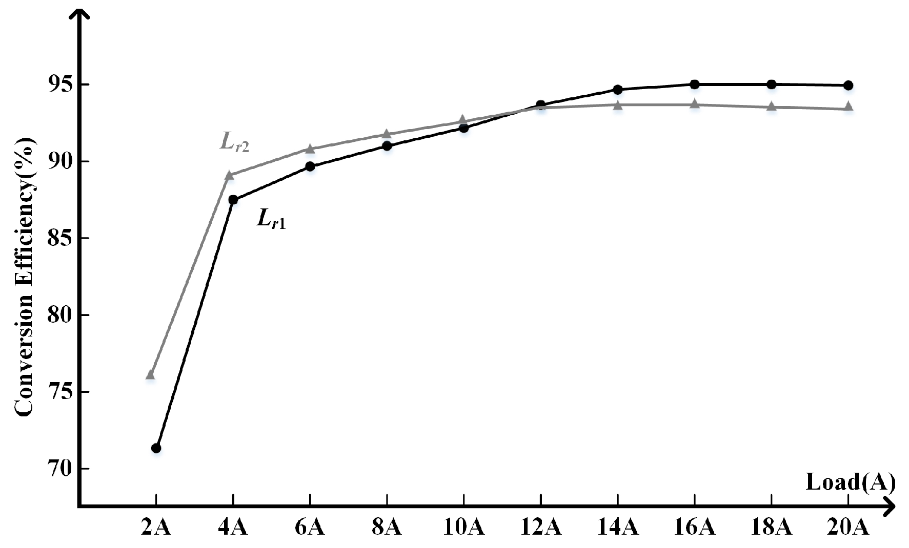
Figure 4 illustrates the potential conversion efficiencies of a PSFBC with two distinct resonance inductor values. Selecting a smaller resonant inductor value is advisable if the PSFBC is frequently operated under heavy loads. Conversely, a larger resonant inductor value is more suitable when the utilization rate primarily consists of light loads. The choice of resonance inductor directly impacts the conversion efficiency of the PSFBC and necessitates an optimal design approach.
The transformer turns ratio is a crucial parameter that influences both the time interval of the energy transfer region and the primary-side current (
ip).
Figure 5 represents simulated waveforms obtained using PSIM for two different transformer turns ratios, namely 13 and 10, where the turns ratio
n is defined as
Np divided by
Ns, as shown in
Figure 1.
Figure 5 shows that an increased turns ratio results in a longer time interval for the energy transfer region, leading to a smaller RMS current of the primary-side current than a smaller transformer turns ratio. The longer time interval for the energy transfer region implies a reduced time interval and decreased loss for the current circulating region. Furthermore, the smaller RMS current of the primary-side current indicates reduced conduction loss.
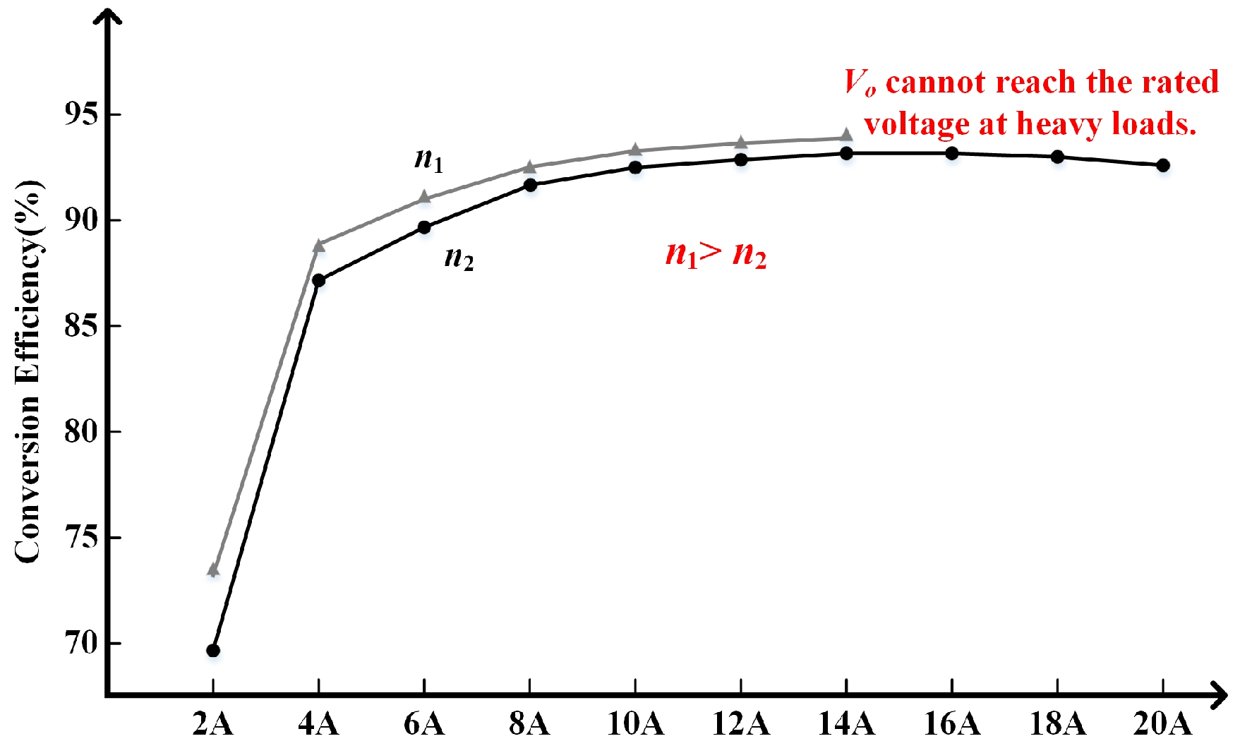
Figure 6 illustrates the potential conversion efficiencies of a PSFBC for two distinct transformer turns ratios, with
n1 being greater than
n2. Selecting a larger transformer turns ratio, represented by
n1 in
Figure 6, can achieve higher conversion efficiency at light loads but may result in a potentially lower output voltage at heavy loads. Conversely, opting for a smaller transformer turns ratio, represented by
n2 in
Figure 6, ensures that the rated output voltage is reached at heavy loads but with lower conversion efficiency.
Figure 4,
Figure 5 and
Figure 6 are general views; therefore, detailed circuit parameters are not listed. Light, medium, and heavy loads in this paper are roughly classified as 0–30%, 30–60%, and above 60%, respectively. The selection of the transformer turns ratio directly affects the conversion efficiency and output voltage of the PSFBC, also necessitating an optimal design approach.
Figure 3,
Figure 4,
Figure 5 and
Figure 6 also show that the transformer turns ratio and resonance inductor value in a PSFBC are mutually interdependent and, therefore, require a simultaneous design approach.
In the past, designing the magnetic components of a PSFBC, such as the transformer turns ratio and resonance inductor value, has been a complex task due to the multitude of possible parameter adjustments and combinations. However, developing a highly accurate digital twin of a PSFBC can facilitate efficient parameter design through simulations. To address this objective, this paper proposes a digital twin for PSFBCs which enables a more precise loss estimation and facilitates optimal parameter design.
3. Accurate Loss Estimation
The proposed loss estimation method provides a precise duty ratio calculation of the energy transfer and circulation regions and the corresponding current points of the primary-side transformer current, leading to enhanced accuracy. Notably, the method incorporates the exciting current of the transformer (iM), thereby improving the precision of the estimated current points for the primary-side transformer current, particularly under light-load conditions. Additionally, an iterative duty ratio adjustment is employed to enhance the accuracy of the loss estimation further. The detailed derivation of the proposed loss estimation method is presented in this section.
To estimate the loss of a PSFBC, it needs to calculate the current points of
i1 to
i6, as shown in
Figure 2, under different load conditions as accurately as possible. Traditionally, the current points,
i1 to
i6, under a specific output current,
Io, can be derived as [
13,
14]
where
and
are the resonant angular frequencies of the leading-leg and lagging-leg switches of a PSFBC, respectively.
is the dead time.
is the turn-on resistance of a power switch. It is worth noting that
i4 is calculated from
i3 with the power switches
S1 and
S3 turned on, as illustrated in
Figure 2. Therefore, the
values of the two power switches are considered in (1d). Other variables in (1) are denoted in
Figure 1 and
Figure 2.
The voltage gain for a PSFBC can be expressed as
The
Deff and
Dcir can be calculated using (8) and (9), respectively.
Note that the conventional method does not take into account the influence of the exciting current of the transformer (
iM). As a result, the accuracy of estimating the current points is significantly degraded, particularly under light-load conditions. From
Figure 2, it can be observed that the current points of
i1 and
i2, taking the
iM into account, can be represented as
The other current points,
i3 to
i6, will be changed according to the modified
i1 and
i2. The
can be estimated by the following derivations. First, the relationship between the currents of
,
, and
can be expressed as
Equation (5) can be approximately estimated as
where
and
are the voltages of
and
, respectively, and can be expressed as
where
is the diode forward voltage. Due to the smaller value of
, the voltage drop across a power switch is generally neglected [
13,
14]. If the voltage drops of power switches are considered, (7a) could be more accurate.
Substituting (7) into (6), (6) can be expressed as
Equation (8) can be rearranged as
Therefore, the
can be expressed as
Incorporating the
calculated using (11) can effectively improve the estimation accuracy of the current points for
i1 to
i6. As depicted in
Figure 2, it is expected that the magnitudes of the current points at
i1 and
i6 should be identical due to the symmetry. However, even with the proposed more accurate calculations, it is still observed that the magnitudes of the current points at
i1 and
i6 do not align. This suggests the need to adjust the duty ratios of
Dcir and
Deff. The initial guess for the duty ratio of
Deff, estimated using Equation (3a), serves as a starting point; however, there is a mismatch in the magnitudes of the current points at
i1 and
i6 in this initial guess. An iterative duty ratio adjustment, as proposed in [
14], is employed in this paper to refine the duty ratio of
Deff further until the magnitude mismatch of
i1 and
i6 falls below a convergence tolerance threshold. Once the current points are calculated, the conduction and switching losses can be straightforwardly determined. These losses can be more accurately calculated based on the precise estimation of the current points. For example, the RMS current of the energy transfer region can be expressed as
where
is the RMS current in the energy transfer region.
The RMS currents for the resonant region of leading-leg switches, the circulation region, the resonant region of lagging-leg switches, and the transition region can also be calculated similarly. Once the RMS currents are obtained, the conduction losses of the circuit can be calculated. The conduction losses in the operating regions of the primary side of the transformer can be written as
where
,
,
,
, and
are the conduction losses for the energy transfer region, resonant region of leading-leg switches, circulation region, resonant region of lagging-leg switches, and transition region, respectively.
,
,
, and
are the RMS currents in the energy transfer, circulation, transition regions, resonant region of leading-leg switches, and resonant region of lagging-leg switches, respectively.
and
are the resistances of
Lr and the primary side of the transformer, respectively.
The conduction losses in the circuit components of the secondary side of the transformer can be approximately calculated using
where
,
, and
are the conduction losses of the secondary side of the transformer, forward diode, and
Lo, respectively.
and
are the resistances of the secondary side of the transformer and
Lo, respectively.
The total conduction loss of a PSFBC can then be calculated by summing (13) and (14) and expressed as
where
is the total conduction loss of a PSFBC.
The switching losses can be calculated based on the drain-source voltage and current flowing through a power switch. The turn-on drain-source voltages for the leading-leg and lagging-leg switches can be approximately estimated using
where
and
are the turn-on drain-source voltages for the leading-leg and lagging-leg switches, respectively.
and
are the equivalent parasitic capacitances for the leading-leg and lagging-leg switches, respectively.
Equation (16) can be used to determine whether ZVS is achieved. If the calculated voltage is less than or equal to zero, ZVS is achieved, and there will be zero switching loss at this output current. The switching losses for the leading-leg and lagging-leg switches and the diodes in the secondary of the transformer can be written as
where
and
are the switching losses for the leading-leg and lagging-leg switches, respectively.
is the switching loss for the diodes on the secondary side of the transformer.
and
are the turn-on and turn-off time intervals of a power switch, respectively. The time intervals can be acquired from the power switch’s specification.
and
are the turn-off drain-source voltages for the leading-leg and lagging-leg switches, respectively. Note that the turn-off drain-source voltages will be close to the
Vin without a hardware topology reinforcement.
and
are the reverse recovery current and time of a diode, respectively.
is the switching frequency of the PSFBC.
The total switching loss of a PSFBC can then be calculated by summing (17) and expressed as
where
is the total switching loss of a PSFBC.
The total loss at a specific output current can be written as
where
is the total loss of a PSFBC under a specific output current.
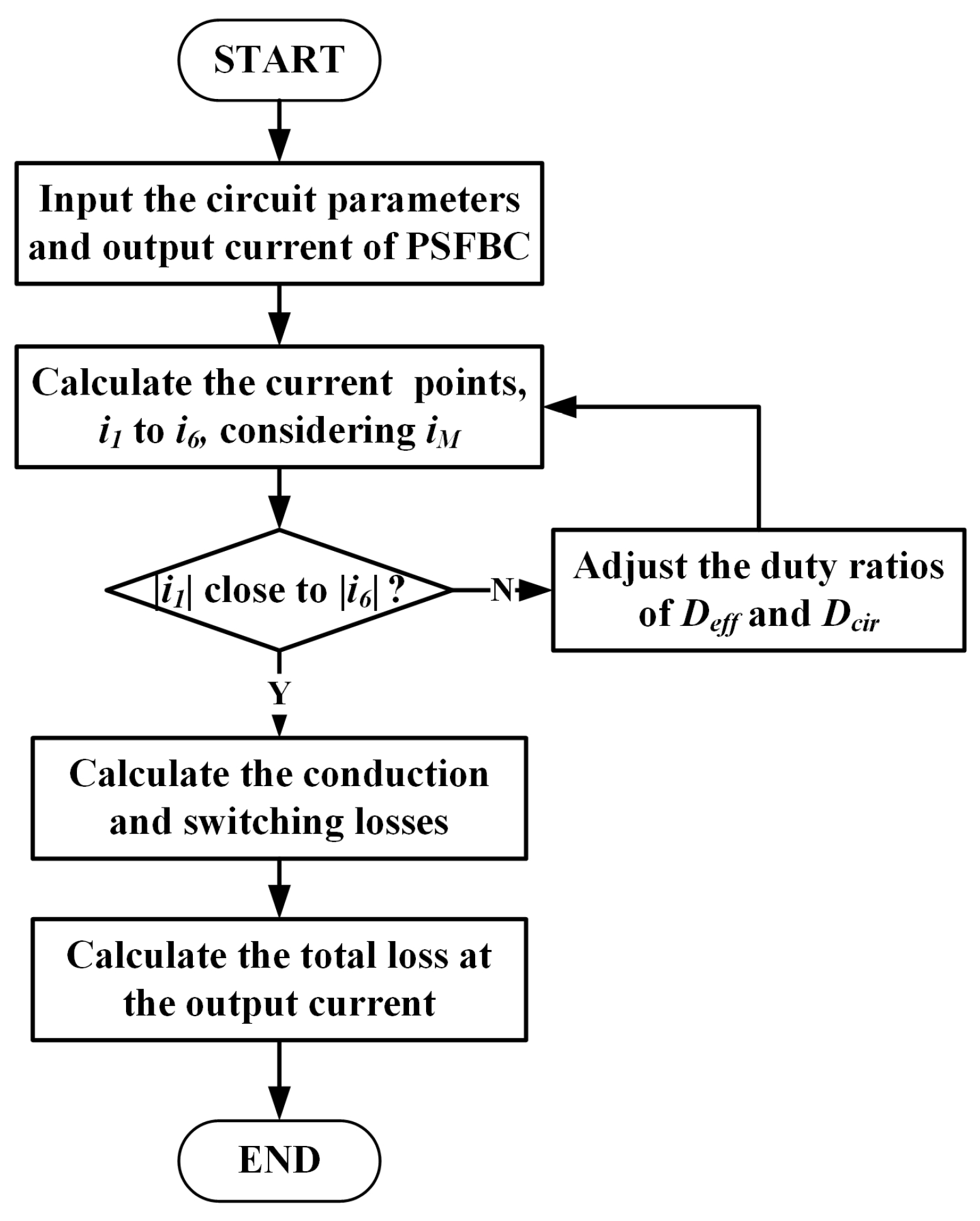
The flowchart in
Figure 7 illustrates the proposed loss estimation process. By utilizing the circuit parameters and the output current of a PSFBC, the current points of
i1 to
i6 can be calculated, taking into account the influence of
iM, using (1) to (11). To minimize the magnitude mismatch between
i1 and
i6, an iterative duty ratio adjustment, as proposed in [
14], is employed to refine the duty ratio of
Deff. When
Deff is adjusted,
Dcir will also change accordingly, causing the current points
i1 to
i6 to adjust. This process will be iterated until the convergence error is reached. Subsequently, the conduction and switching losses can be determined using (12)–(15) and (16)–(18), respectively. Finally, the total loss at the output current is obtained through (19). Most parameter variations in a PSFBC circuit, such as voltage, current, and losses, can be calculated using the abovementioned formulas. Therefore, a digital twin of a PSFBC, serving as a virtual representation of the PSFBC and allowing for easy adjustments and replacements of circuit components and parameters without additional effort, will be described in
Section 4.
4. Digital Twin of PSFBC and Parameter Optimization of Magnetic Components
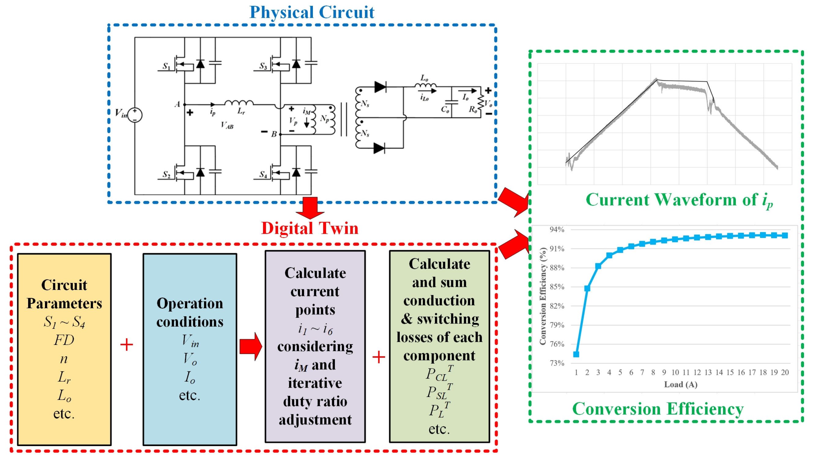
Designing the magnetic components’ parameters of a PSFBC, such as the transformer turns ratio and resonance inductor value, is complicated due to the numerous possible parameter adjustments and combinations. However, developing a highly accurate digital twin for a PSFBC can facilitate efficient parameter design through simulations.
Figure 8 illustrates the concepts of the proposed digital twin for PSFBCs, utilizing the precise current points and loss estimation derived in
Section 3. It is important to note that while the physical circuit can provide the most accurate experimental waveforms and conversion efficiency, assessing performance variations with adjustments or replacements of circuit components becomes challenging. A digital twin of a PSFBC serves as a virtual representation of the physical circuit, allowing for straightforward adjustment and replacement of circuit components and parameters without additional effort, given that the digital twin has been appropriately designed with sufficient accuracy. As depicted in
Figure 8, the proposed digital twin of a PSFBC considers the circuit parameters and operating conditions to estimate the current waveform of
ip accurately. Following acquiring the current waveform and points for the primary-side transformer, the detailed conduction and switching losses for each circuit component can be calculated. Consequently, the losses of each component and conversion efficiencies under different load conditions can be estimated. Any adjustments to circuit parameters and operating conditions can be easily observed through the proposed digital twin without hardware modifications. The proposed digital twin proves to be highly beneficial for PSFBC design, particularly for parameter adjustment and component selection. This paper specifically focuses on the design of magnetic components, namely the transformer turns ratio and resonance inductor value, for a PSFBC.
Figure 9 illustrates the application of the proposed digital twin in the magnetic component design of a PSFBC for operational loss minimization. The control variables for the digital twin are the potential transformer turns ratios and resonance inductor values, while the other components and specifications of the PSFBC have already been determined. Each combination of transformer turns ratios and resonance inductor values is an input for the digital twin, generating a corresponding conversion efficiency curve. Furthermore, the output voltage can be easily calculated using (2) for different load conditions, as the iterative duty ratio adjustment estimates the duty ratio for the energy transfer region. This enables the optimal design to maintain the rated output voltage under varying load conditions.
The PSFBC is designed for use in diverse scenarios, such as server power supplies or chargers, where the load conditions result in different utilization rates.
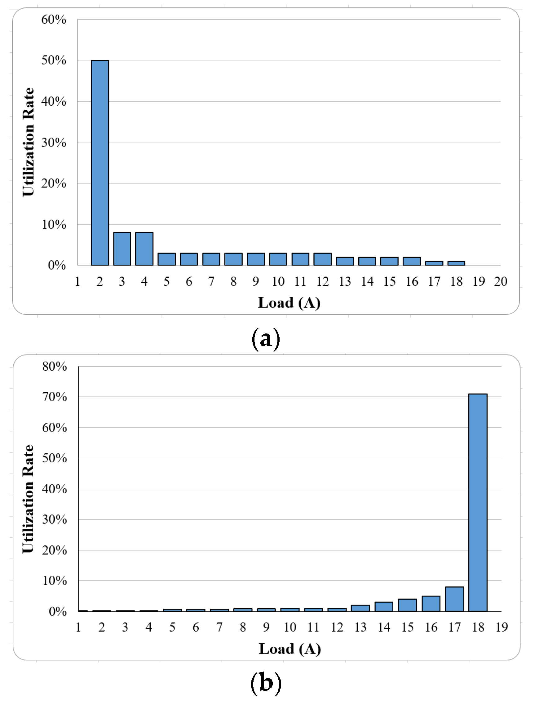
Figure 10 illustrates the potential load utilization rates for a server power supply and a charger. The possible utilization rates of a server power supply, as depicted in
Figure 10a, are a statistic from a Web 2.0 server where the high utilization rate indicates a more extended time [
20]. The potential utilization rates of a charger are determined based on statistical data obtained while charging a Li-ion battery using the PSFBC prototype implemented in this paper.
Figure 10 shows that the server power supply operates mainly under light-load conditions, whereas the charger operates under heavy load conditions. By comparing
Figure 10 with
Figure 3 and
Figure 5, it becomes evident that different resonance inductor values and transformer turns ratios need to be considered to minimize the operational losses of the PSFBC for different application scenarios. The operational loss for an application scenario of the PSFBC can be calculated by the output powers with the corresponding load utilization rates and conversion efficiencies and then summing them up and expressed as
where
is the operational loss of a PSFBC for the application scenario.
,
, and
are the utilization rate, output power, and conversion efficiency of the PSFBC under the
kth load condition.
The proposed digital twin can select the optimal combination of transformer turns ratio and resonance inductor value that minimizes the operational loss of the PSFBC for a specific application scenario from the possible combinations. The grid search is used in this paper. It is worth mentioning that heuristic algorithms, such as genetic algorithms, particle swarm optimization, ant colony algorithms, and others, can be employed to expedite finding the optimal combination that minimizes operation loss. However, since this paper focuses on developing the digital twin, the investigation of heuristic algorithms will be pursued in future research.
5. Experimental and Simulation Results
In this paper, a PSFBC prototype is designed and implemented. The PSFBC prototype has a rated input voltage of 380 V, a rated output voltage of 24 V, and a rated output current of 20 A. The parameters of the PSFBC prototype are listed in
Table 1. In this section, experimental investigations are conducted to examine the influences of the transformer turns ratios and resonance inductor values on the voltage and current waveforms of the PSFBC, as well as to validate the proposed loss calculation. The proposed digital twin is then employed to simulate and identify the optimal transformer turns ratio and resonance inductor value.
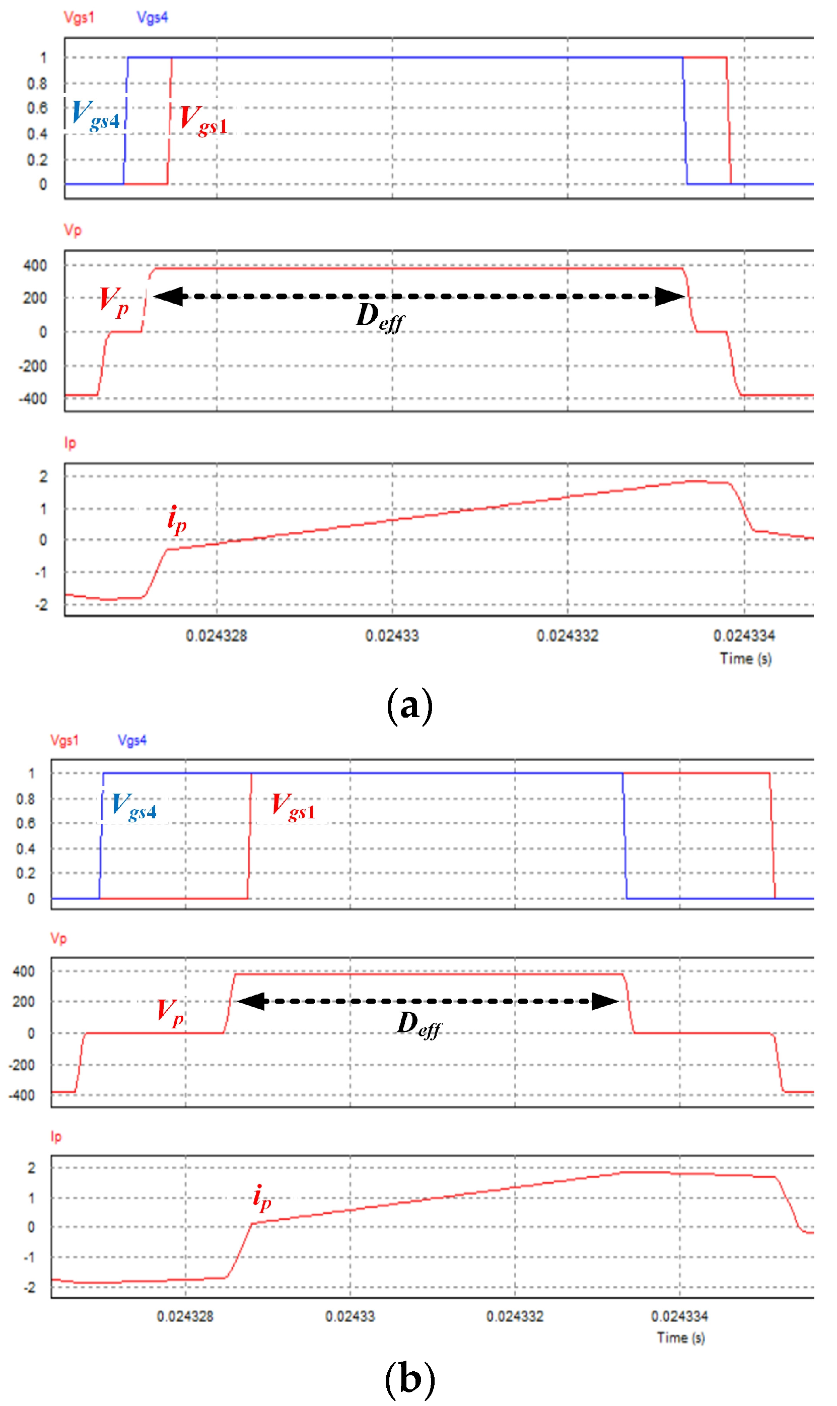
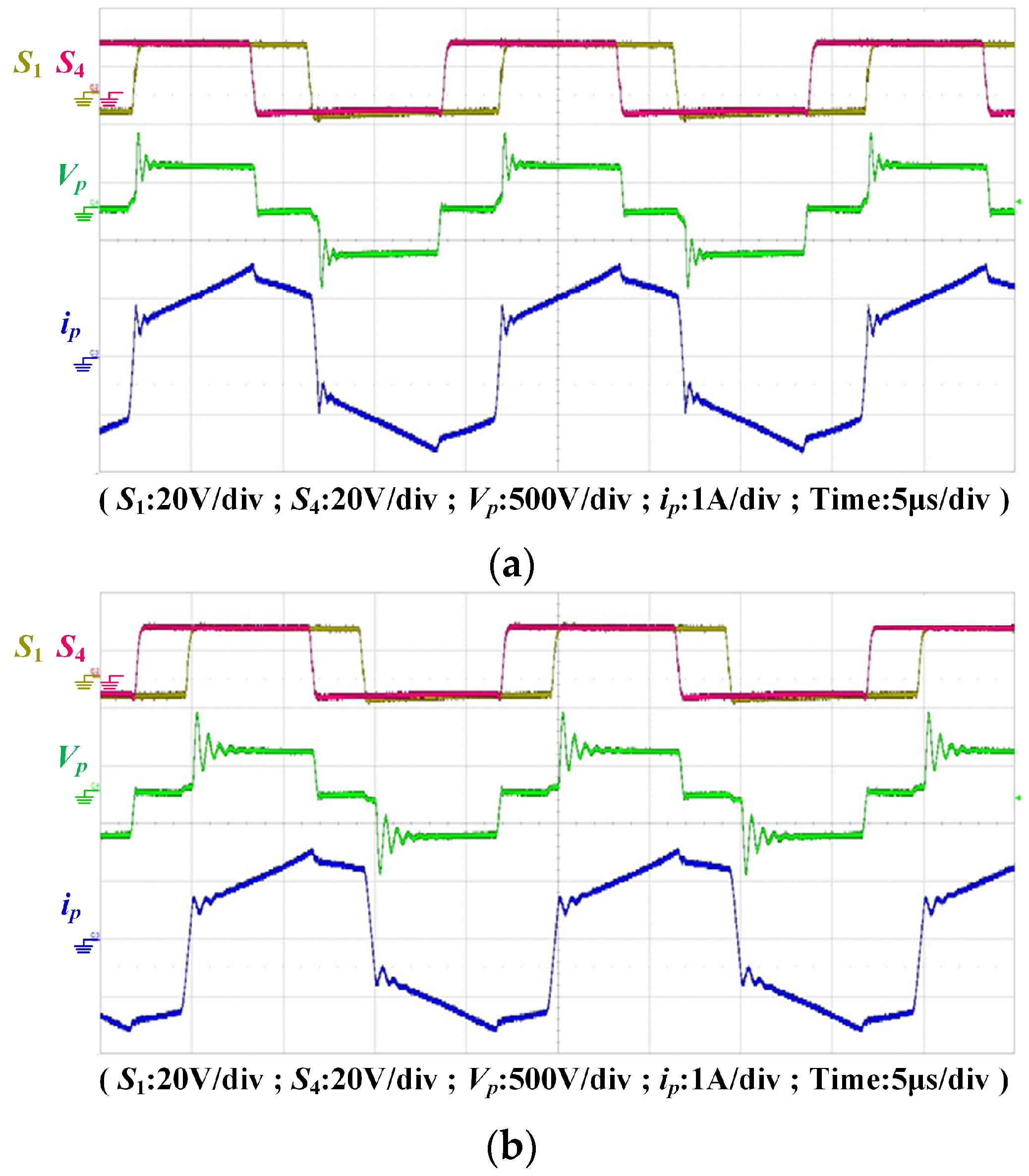
Figure 11a,b represent the experimental waveforms of the PSFBC prototype at an output current of 10A, with a transformer turns ratio of 10 and resonance inductor values of 34 µH and 83 µH, respectively. It is observed that
Figure 11b, with the larger inductor value, exhibits a slightly slower current rise in the transition region compared to
Figure 11a, with the smaller inductor value. Consequently,
Figure 11b has a slightly longer time interval for the transition region. Additionally, the larger inductor value in
Figure 11b leads to a gradual decline in the current during the circulating region, resulting in a higher RMS current in the circulating region compared to
Figure 11a. Thus, a larger resonance inductor value amplifies conduction loss while potentially reducing switching loss, making it preferable for a PSFBC that frequently operates under light loads. Conversely, a smaller resonant inductor value is more suitable when the utilization rate primarily consists of heavy loads. Similarly,
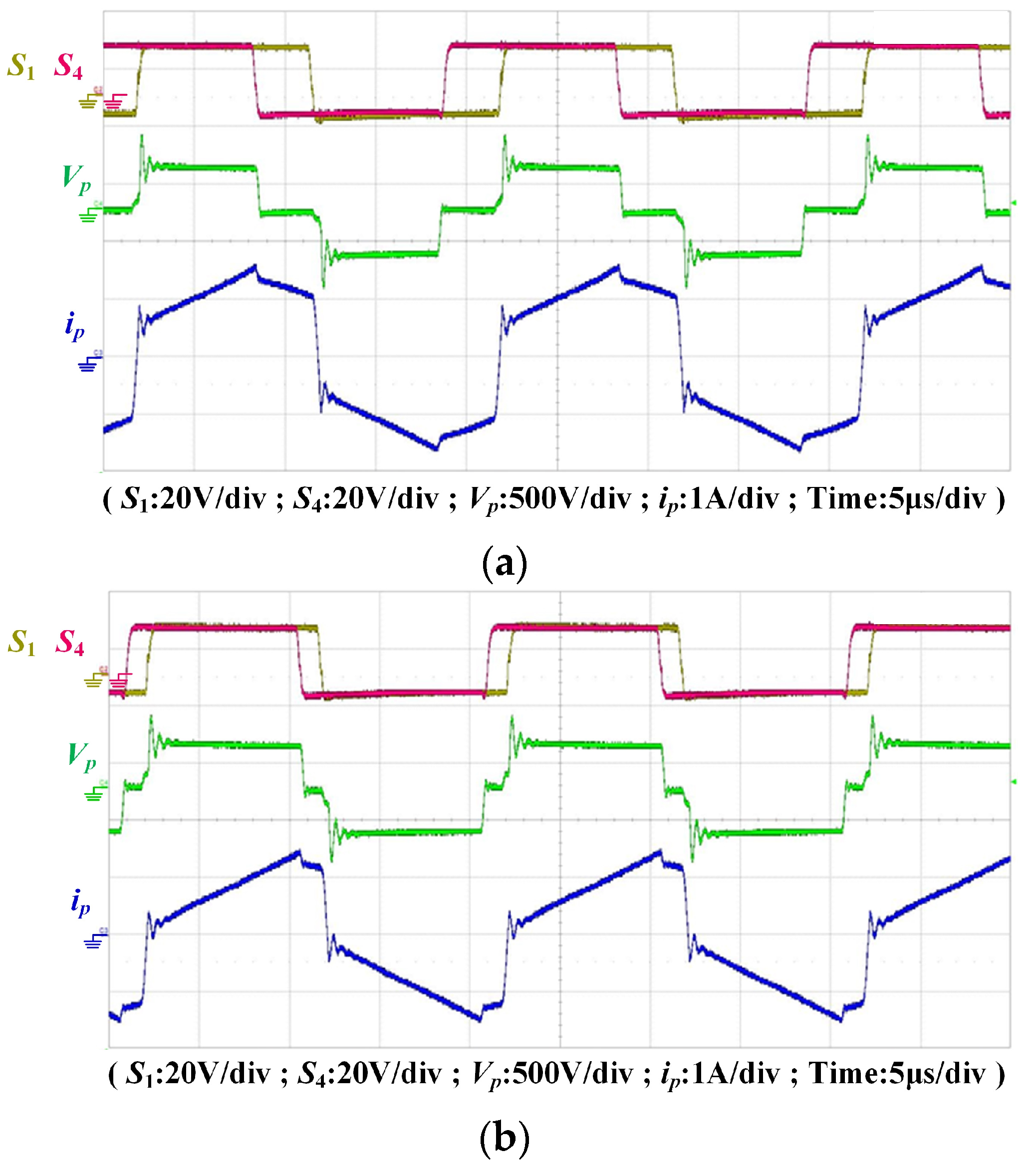
Figure 12a,b demonstrate the experimental waveforms of the PSFBC prototype at an output current of 10 A with a resonance inductor value of 34 µH and transformer turns ratios of 10:1 and 13:1, respectively. The transformer turns ratio affects both the time interval of the energy transfer region and the primary-side current.
Figure 12b shows that an increased turns ratio results in a longer time interval for the energy transfer region, leading to a smaller RMS current of the primary-side current compared to a smaller transformer turns ratio in
Figure 12a. The longer time interval for the energy transfer region implies a reduced time interval and decreased loss for the current circulating region. Furthermore, the smaller RMS current indicates reduced conduction loss. Choosing a larger transformer turns ratio, as depicted in
Figure 12b, can achieve higher conversion efficiency but may result in a potentially lower output voltage at heavy loads. On the other hand, opting for a smaller transformer turns ratio ensures that the rated output voltage is maintained at heavy loads, albeit with lower conversion efficiency. From
Figure 11 and
Figure 12, it can be observed that transformer turns ratios and resonance inductance significantly affect the PSFBC performance. The selection of the transformer turns ratio directly affects the conversion efficiency and output voltage of the PSFBC, emphasizing the need for an optimal design approach.
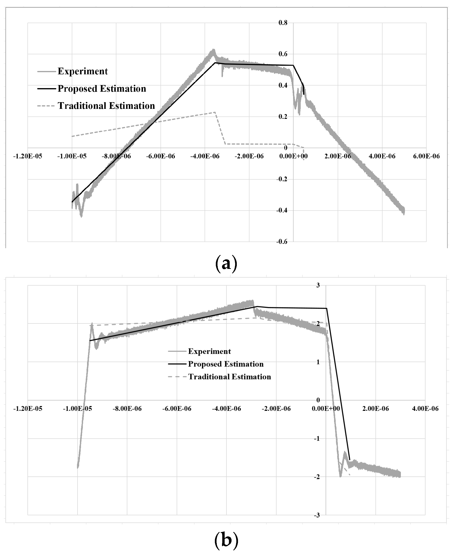
Figure 13a,b depict the measured and estimated primary-side current waveforms at an output current of 1 A and 20 A, respectively.
Table 2 represents the current points,
i1 to
i6, measured from the PSFBC prototype, estimated using the proposed loss estimation method and calculated using the traditional method [
14] without considering the exciting current of the transformer and iterative duty ratio adjustment.
Table 2 shows that the proposed current points closely match the measured currents, even at light loads. This demonstrates the accuracy of the proposed loss estimation in accurately estimating the current points of
i1 to
i6.
Figure 14a,b display the measured and estimated conversion efficiencies of the PSFBC prototype with the resonance inductor value of 83 µH and transformer turns ratios of 10 and 13, respectively.
Figure 14 indicates that the proposed loss estimation method exhibits a similar trend to the measured conversion efficiency curves. While there are some estimated conversion efficiency errors at the light loads, the proposed loss estimation method offers higher accuracy. Therefore, it can be utilized in constructing a digital twin for PSFBCs to simulate the optimal design of transformer turns ratio and resonance inductor value.
Figure 10 represents the utilization histograms for different application scenarios, namely server power and battery charger. By utilizing the proposed digital twin of PSFBCs, the optimal transformer turns ratio and resonance inductor value can be determined to minimize the operational loss for each application scenario. It is important to note that the transformer turns ratio and resonance inductor value in a PSFBC are mutually interdependent and require a simultaneous design approach. The range of potential transformer turns ratios for optimal design is between 9 and 13 with a step of 0.1, while the range of possible resonance inductor values is between 40 µH and 130 µH with a step of 1 µH. This results in a total of 3600 possible combinations. The range and step size for the transformer turns ratio and resonance inductor value can be adjusted according to specific requirements. Due to the page limit, the parameter optimization of magnetic components in this paper only considers the fixed switching frequency and transformer core material for the implemented PSFBC. The proposed digital twin can also take different switching frequencies and materials of the transformer core into account, and this will be conducted in future research. Each combination can be analyzed using the procedures outlined in
Figure 9, and the operational loss can be calculated using (20). The optimal designs for minimizing operational loss of each application scenario are solved and listed in
Table 3. From
Table 3, it can be observed that magnetic components should be carefully designed for different application scenarios to reduce operational loss. Using the charger as an example, the charger, in most cases, operates under constant-current charging and experiences heavy load conditions. After simulations, the optimal transformer turns ratio and resonance inductor value are determined to be 12.3 and 45 µH, respectively. The estimated operational loss per hour is approximately 30.825 Wh. In contrast, if a transformer turns ratio of 9 and a resonance inductor value of 30 µH are casually designed for the PSFBC, the total operational loss per hour would be 35.724 Wh. The proposed resonance inductance design can reduce operational loss by about 14%.
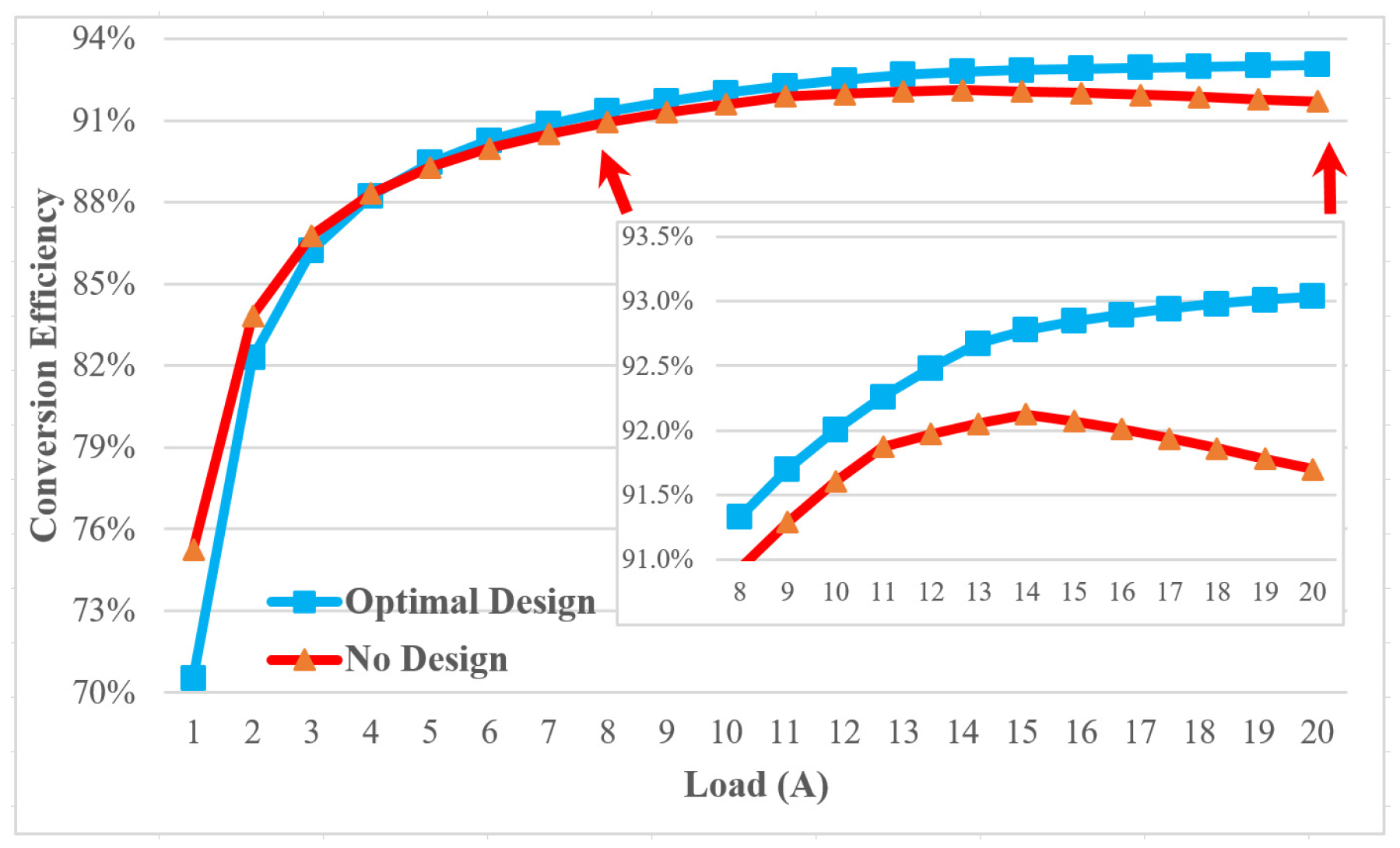
Figure 15 illustrates the conversion efficiencies of the optimal and casual designs, as simulated by the proposed digital twin. The performance of the proposed digital twin of PSFBCs in parameter optimization of magnetic components is clearly observed and demonstrated. Different parameter designs for PSFBCs can be found in [
5,
6,
7,
8,
9,
10,
11,
12,
13,
14,
15]; however, these methods do not consider accurate digital twins or the application scenarios of PSFBCs, resulting in designs that are closer to the casual design in
Figure 15 and thus unable to achieve optimal parameter design results. The digital twin proposed in this paper can be applied to various converters, such as multi-port topologies [
21], and will be investigated in future research. More detailed circuit analysis and obtaining correct circuit parameters are necessary to enhance the accuracy of a digital twin. The correction of converter parameters constitutes the primary limitation of the proposed digital twin and will also be further studied.


