Review

A Review on Buried Interface of Perovskite Solar Cells

1
State Key Laboratory of Solidification Processing, Northwestern Polytechnical University, Xi’an 710072, China
2
Research & Development Institute, Northwestern Polytechnical University, Shenzhen 518057, China
*
Author to whom correspondence should be addressed.
Energies 2023, 16(13), 5015; https://doi.org/10.3390/en16135015
Submission received: 29 May 2023 / Revised: 19 June 2023 / Accepted: 26 June 2023 / Published: 28 June 2023
(This article belongs to the Topic Photovoltaic Materials and Devices)

Abstract

:
Perovskite solar cells (PSCs) have been developed rapidly in recent years because of their excellent photoelectric performance. However, interfacial non-radiative recombination hinders the improvement of device performance. The buried interface modification strategy can minimize the non-radiation recombination in the interface and can obtain the high efficiency and stability of PSCs. In this review, we introduce the device structure and the charge carrier dynamics (charge transfer, extraction, and collection) at the interface. We further summarize the main sources of non-radiative recombination at the interface, such as energy alignment mismatch and interface defects, and methods to characterize them. In contrast to the previous review of perovskite solar cells, the important roles of buried interfaces in regulating energy level alignment, passivating surface defects, modulating morphology, and so on are reviewed in detail based on the latest research, and strategies for reducing interfacial nonradiative recombination are provided. In the end, the potential development and challenges of buried interfaces for high-performance and stable PSCs are presented.

1. Introduction

Organic–inorganic hybrid perovskite solar cells (PSCs) have attracted much attention because of their advantages, such as tunable bandgap [1], high charge carrier mobility [2], high light absorption coefficient [3], and low exciton binding energy [4]. Since Miyasaka et al. [5] in 2009, the first attempt to use a halide perovskite as a sensitizer in dye-sensitized solar cell structures, PSCs have achieved remarkable progress in the last decade, with a rapid increase in power conversion efficiency (PCE) from a previously reported 3.8 percent to a current 25.7 percent [6]. Figure 1 illustrates the efficiency evolution of perovskite-type solar cells [7], which is equivalent to today’s industrial-grade single-crystal silicon solar cells. This outstanding efficiency, combined with the processing characteristics and low manufacturing cost of perovskite solutions [8], makes it a promising candidate for the next generation of thin-film solar cells.
Although PSCs have developed rapidly, their efficiency remains far below their Shockley–Queisser (SQ) maximum theoretical efficiency (>30%) [9]. The SQ limit efficiency is based on the condition that each carrier recombination is radiative; thus, to improve the PCE value, non-radiative recombination that causes energy loss must be reduced. Currently, PSCs are largely divided into planar heterojunction structures and mesoporous structures. Each structure typically includes a conductive glass/electron transport layer (ETL)/perovskite (PVK)/hole transport layer (HTL)/precious metal electrode [10]. Defects and energy level mismatch in the PVK interface (ETL/PVK interface, PVK/HTL interface) are the main sources of nonradiative recombination, which influences the final performance of the device [11,12]. Minimizing non-radiative recombination at the interface is crucial for PSCs with high efficiency and stability.
In this review, we only focus on solar cells with n-i-p structures. At present, for solar cells with n-i-p structures, the study of interfaces is mainly concerned with the stabilization of the top interface, i.e., the perovskite/HTL interface, through post fabrication and HTL modification [13,14,15,16]. However, the buried interface, which is the interface between the electron transport layer (ETL) and the perovskite layer, may have even higher defect concentrations than that of the top interface [17]. Therefore, research on buried interfaces is particularly important. However, testing and characterizing buried interfaces of perovskite films are very difficult and lack in-depth understanding; thus, they have received little attention [18,19,20]. The situation of the buried interface of solar cells with a p-i-n structure is similar to that.
In this paper, the recent progress and future research on buried interface modifications are summarized. We outline the influence of interface carrier dynamics on device performance, summarize the reasons for non-radiative recombination in PSCs, and concentrate on the main sources of non-radiative recombination on the interface. We systematically review the regulation of PSCs’ energy levels, the passivation of interface defects, and the regulation of perovskite film morphology by buried interface modification. Finally, we briefly discuss the development direction of buried interface modification in order to produce high-efficiency and stable PSCs.

2. Device Structure

The light-absorbing material of a perovskite solar cell is an organic–inorganic hybrid perovskite structure material with a chemical formula of ABX3, where A is the organic cation or an inorganic metal cation (CH3NH3+,CH(NH2)2+ and Cs+); B is usually the metal cation (Pb2+, Sn2+); X is the halide anion (I, Br and Cl) [21]. In the ABX3 crystal, BX6 forms a regular octahedron, and BX6 is linked by sharing vertices X to shape a three-dimensional skeleton. A is embedded in the octahedral voids to stabilize the crystal structure [22], as shown in Figure 2a. For the formation of a stable hybrid perovskite cubic structure, the size of the A cation needs to be restricted to the interstitial space between the BX6 inorganic metal halide octahedra, which places high demand on the spatial geometric size of the ions. Even slight distortions and distortions in the structure reduce the symmetry of the perovskite material, and the coordination numbers of A and B cations also decrease. In general, the stability of the perovskite structure is decided by the tolerance factor (t) and the octahedral factor (μ) of the material [23]; Figure 2b shows the tolerance factor (t) of a perovskite crystal [24].
tolerance   factor : t = r A + r B 2 r B + r X
octahedral   factor : μ = r B r X
where r A , r B , and r X are, respectively, the radii of ions A, B, and X.
The tolerance factor developed by Goldschmidt [23] is commonly used as a criterion for predicting crystal structure. What’s more, he found that ABX3-type materials based on halogens could only form stable perovskite structures when their tolerance factor is in the range of 0.81 ≤ t ≤ 1.1 and their octahedral factor is in the range of 0.44 ≤ μ ≤ 0.90. When the tolerance factor is greater than 0.89 but less than 1, the perovskite structure is cubic. The closer the tolerance factor is to the ideal value, the closer the perovskite crystal structure approaches the highly symmetric cubic perovskite structure (Figure 2c) [24]. When the tolerance factor deviates from the ideal amount, the crystal structure undergoes distortion, and the perovskite structure may transform into a tetragonal or orthorhombic phase, which is detrimental to the preparation of solar cells [25].
PSCs structures are generally classified into two kinds: mesoporous or planar structures. The mesoporous structure is similar to that of dye-sensitized solar cells and was initially applied to early versions of PSCs. The cell structure from top to bottom consists of a transparent electrode (FTO/ITO)/dense layer of TiO2/porous layer of TiO2/perovskite layer/hole transport layer, as well as a metallic electrode. In the mesoporous structure, the hole transport material partially fills the gap between the titanium dioxide and the perovskite layer, making the TiO2 particles with the electron transfer function come into direct contact with the hole transport layer, resulting in leakage current as well as decreased open-circuit voltage. In the planar structure, the perovskite layer is positioned in the middle of p-type and n-type materials, forming a “sandwich” structure. Usually, when depositing the ETL on the conductive substrate, the conductive substrate is the negative electrode, and this structure is considered an n-i-p structure. When depositing HTL on the conductive substrate first, the conductive substrate is the positive electrode, which is considered a p-i-n structure (Figure 2d–f) [26,27,28]. Compared with mesoporous structures, planar structures of PSCs have simpler, more flexible device structures and higher open-circuit voltage, and more and more relevant literature has been reported.
Figure 2. (a) Cubic crystal structure for metal halide perovskite [26]. (b) Tolerance factor (t) equation and ionic radii of common substances [24]. (c) Tolerance coefficient distribution of common perovskites [24]. (d) n-i-p mesoporous structure. (e) n-i-p plane structure. (f) p-i-n plane structure [26].
Energies 16 05015 g002

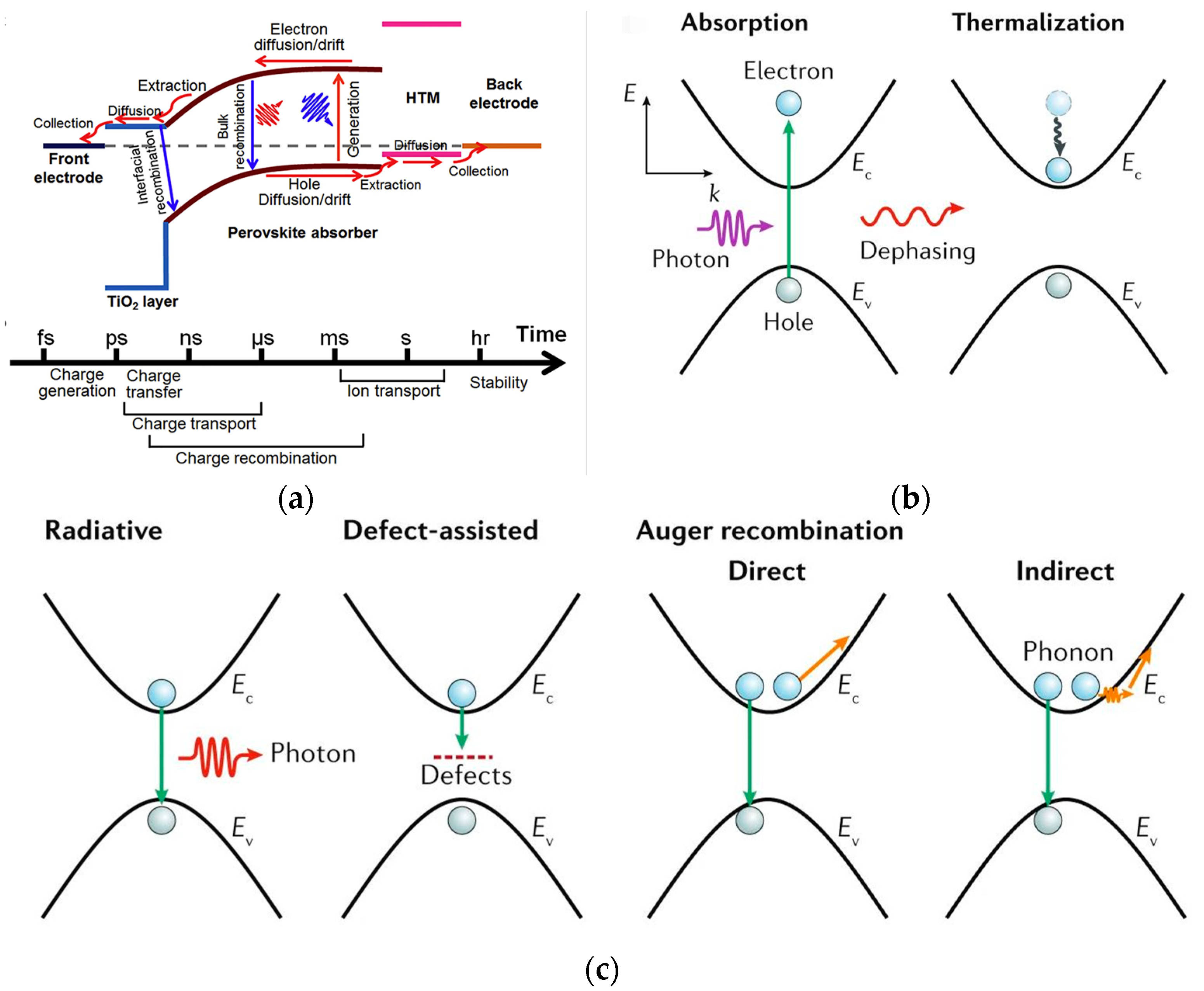
3. Carrier Dynamics in Interface

High efficiency solar cell materials should absorb a wide range of spectra to produce highly efficient electric charges and transfer them to electrodes with minimal losses. Carrier dynamics in PSCs include a lot, such as charge dissociation, charge transport, charge extraction, charge recombination, charge accumulation, and charge collection, as shown in Figure 3a with corresponding time scales [29,30]. The excitation, relaxation, and transport of carriers occur on an extremely short timescale (picosecond scale) [31,32]. When the photon energy is equivalent to or above the bandgap, electrons in the valence band transition to the conduction band. The interaction between excitons is called exciton binding energy, which is low in perovskites, and excitons spontaneously dissociate into free carriers upon photoexcitation [33,34,35]. In addition, some of the carriers are excited to an energy position above the conduction band minimum (CBM) and valence band maximum (VBM) or are pumped to high-energy sub-bands to form hot carriers [36]. These heat carriers are released to the CBM or VBM via electron–phonon interaction [37].
The process of free charge carrier transportation through diffusion or drift in the absorber of a perovskite typically takes several nanoseconds [38,39], and there are dynamic and competitive conditions between the transport and the recombination processes [40,41]. Charge recombination includes radiative and non-radiative recombination [42]. During radiative recombination, perovskites emit photons from the system, the size of which depends on the product of the hole concentrations and electron. Radiative recombination is inevitable, but it has subtle influence and could be ignored. The radiative recombination rate is much smaller than the non-radiative recombination rate, which consists of the Shockley-Read-Hall recombination and the Auger recombination. The transport and recombination of carriers described previously are shown in Figure 3b,c [43]. The course of non-radiative and radiative recombination can be described as follows [44]:
d n d t = k 1 n k 2 n 2 k 3 n 3
Figure 3. (a) Possible charge behavior in the corresponding time scale after light excitation [30]. (b) Hot carrier thermalization and cooling after photoexcitation. (c) Charge recombination dynamics, including radiation recombination, defect assisted recombination, and direct and indirect auger recombination [43].
Energies 16 05015 g003
In the equation, k 1 , k 2 , and k 3 are the rate constants associated with the defect auxiliary (single particle), radiative (two-particle), and Auger (three-particle) recombination processes, respectively, and n is the density of photogenerated carriers. Defect-assisted recombination is dependent on the energy depth and density of the defect, whereas the Auger recombination mainly takes place in perovskite absorbers with high carrier concentrations [45,46,47,48,49]. At the interface, minimizing defects and surface states is expected to reduce SRH recombination [50], and a larger Schottky barrier selectively extracts majority carriers and blocks minority carriers [51,52].
After charge dissociation and transfer, charge extraction occurs rapidly on a picosecond timescale. Charge extraction (injection) has a direct relationship with the incident photon-to-current conversion efficiency (IPCE) as well as Jsc. IPCE is defined as IPCE = η L H E × η i n j × η c c , where η L H E is the light capture efficiency, η i n j is the electron injection yield, and η c c is the charge collection efficiency [53]. As discussed above, the extraction efficiency of the interface charge is primarily decided by the ELA, which relies on the location of the adjacent interface materials. Good energy level alignment can produce an appropriate built-in potential, which is beneficial for charge transfer. In general, it is believed that an energy shift of approximately 0.2 eV is required in order to ensure resultful charge extraction on the ETL/perovskite and perovskite/HTL interface [45].
Charge extraction and ion migration defects are the main causes of charge accumulation, which occurs on a time scale exceeding one second. The accumulation of charge affects electrode polarization, interface energy level mismatch, built-in electric fields, as well as back charge transfer that is near the interface [29,54]. In addition, it has been shown that the main source of J-V hysteresis is caused by the accumulation of interface charges from the interfacial defects and ions, rather than by ion migration in the perovskite thin film during the charge-discharge 169 dynamics [55,56]. After being extracted, the charges need to be collected by the electrode within a few microseconds [57]. The charge transfer efficiencies at the working electrode/ETL interface and HTL/counter electrode interface, as well as the electrode material conductivity, mainly determine the charge collection. If the base electrode is made of FTO or ITO, and the top electrode of the CTL is made of metal Au or Ag, then the efficiency of charge collecting is generally high [58].
As discussed above, charges need to be transferred through multiple layers and through two interfaces (the charge extraction and collection interfaces), which can be seen as a series circuit. From this, the overall internal quantum efficiency (IQE) of the PSCs could be deduced as IQE = η E × η C , where η E is the charge extraction efficiency, and η C is the charge collection efficiency. These are determined by interface charge-carrier dynamics. To achieve a high IQE, it is necessary to have a high charge extraction as well as a low recombination rate, which in turn needs suitable interface energy structures, charge distribution, and atomic bonding [30]. Therefore, charge carrier dynamics are crucial to device performance.

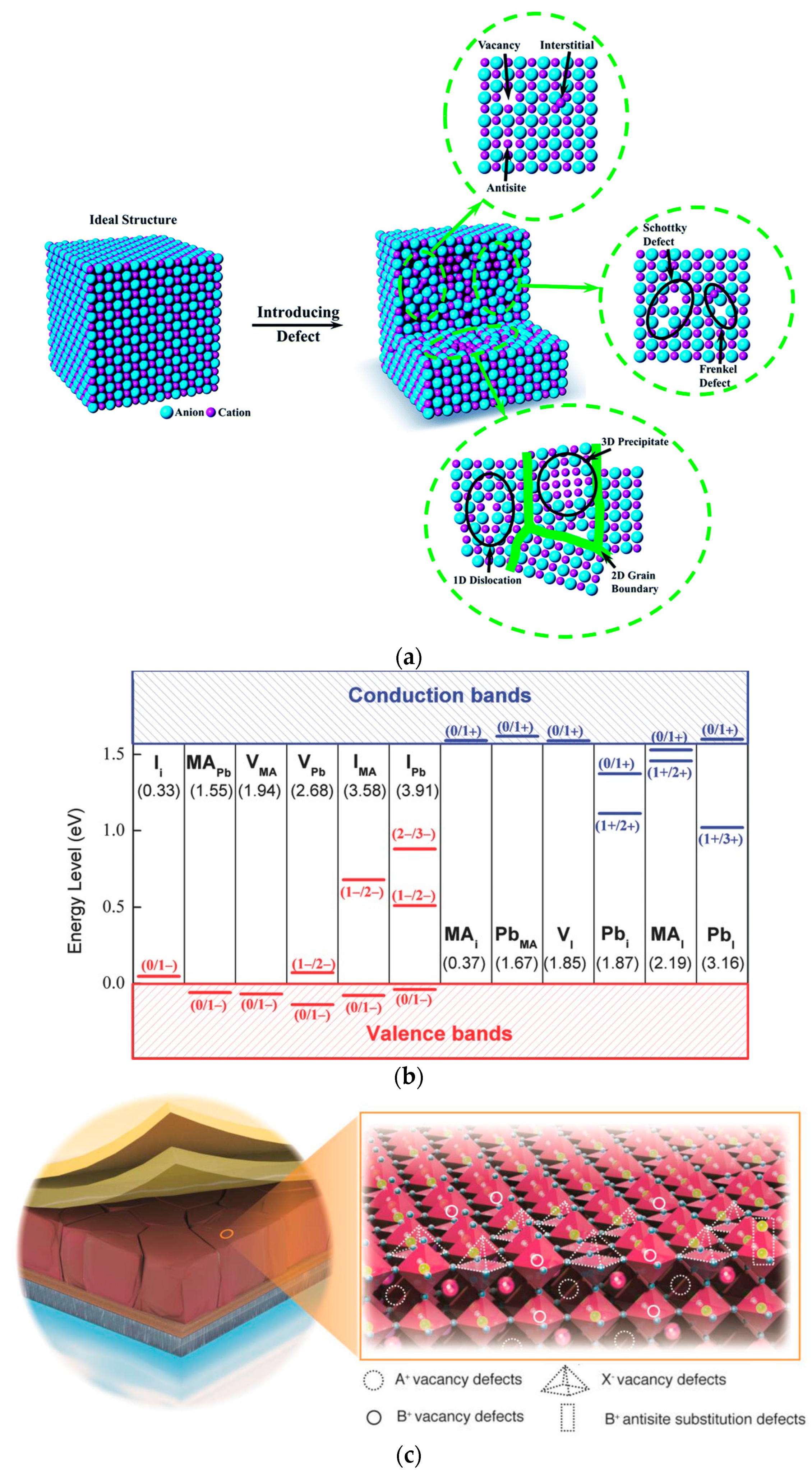
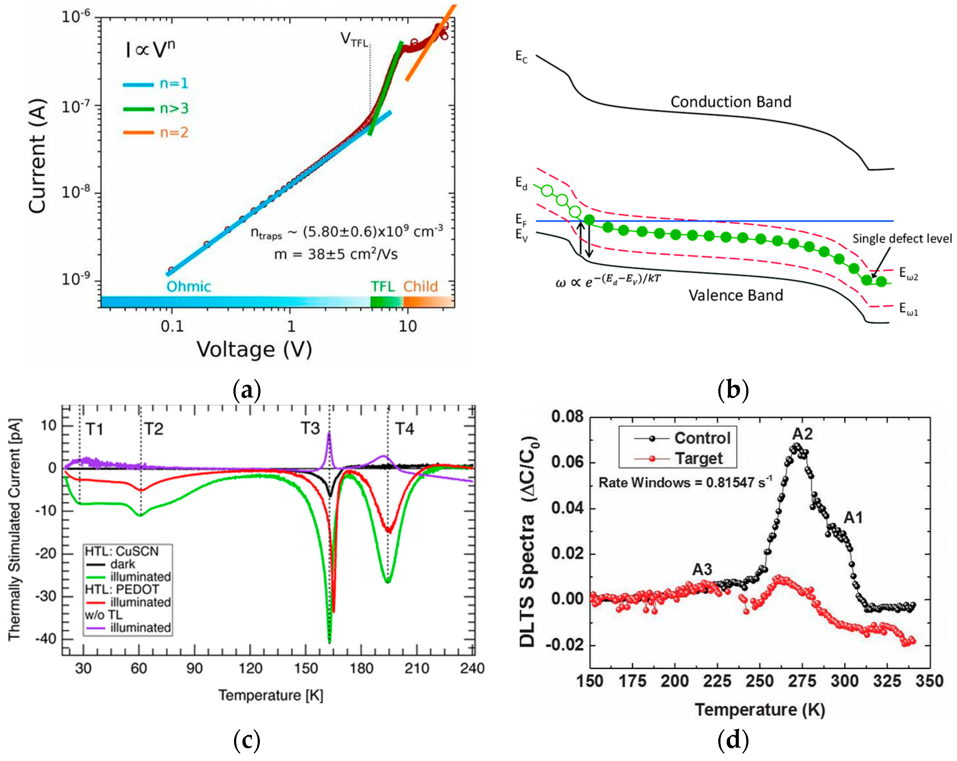
4. The Formation Causes and Characterization Methods of Interface Defects

The high defect densities in the carrier transport layer (CTL) and the perovskite layer capture carriers, leading to interfacial non-radiative recombination, resulting in a decrease in PCE and stability. Currently, many studies pay attention to the top surface of the perovskite layer [14,59] because it is difficult to expose the buried interface and characterize it accurately [60]. However, the accumulation of defects is more concentrated at the buried interface than at the top interface, making the study of buried interface defects more important [61]. The delamination process proposed by Zhu et al. [18] (Figure 4a) can reveal the buried interface at the perovskite thin film. Macroscopically, combining the interface and surface characterization reveals that the losses at the buried interface are caused by sub-micron defects and inhomogeneities. SEM images show that there are more and larger lead halide plate-like particles at the bottom than at the top (Figure 4b), and further analysis using nanoscale Fourier-transform infrared spectroscopy (nano-FTIR) and PL reveal that the lateral concentration inhomogeneity of the main organic cations is more pronounced at the bottom than at the top (Figure 4c). Sub-micron defects and inhomogeneities are involved in the non-radiative recombination center, limiting the performance of the device.
From a microscopic perspective, in an ideal semiconductor crystal structure, every atom is in the right position, with no defects or impurities (Figure 5a). However, due to the solution deposition method used to prepare perovskite thin films and the subsequent rapid crystallization annealing process, a large number of unavoidable defects exist in the actual prepared semiconductor. Figure 5a shows three types of point defects (vacancies, interstitials, and antisites) [62,63], which can be intrinsic or introduced by foreign atoms. In addition to point defects, Figure 5a shows two types of defect pairs (Frenkel and Schottky defects) [64]. The point defects and defect pairs consist of a range of dimensional defects, as shown in Figure 5a, such as 1D defect dislocations formed along the crystal, 2D defects formed at the grain surfaces and boundaries, and 3D defects that may lead to volume changes in the crystal. The 3D defect contains precipitates (tiny volumes with various crystal structures), second phase domains, and large voids [65,66].
Currently, first-principles calculations are commonly used to calculate the theoretical formation energy of point defects [67,68]. Yin et al. [69] theoretically calculated the energy level positions of point defects within MAPbI3, as shown in Figure 5b. Among them, most of the point defects in MAPbI3 are shallow-level defects, where the difference between the ground-state energy level of the defect and the migration edge of the valence band or conduction band is equal to or less than the thermal excitation energy kBT at room temperature [70]. Only IMA, IPb, PbI, and Pbi are deep-level defects within the perovskite bandgap, where the energy difference is larger than kBT [71]. Deep-level defects can capture electrons or holes, which are unable to escape by thermal activation and are eliminated by carrier recombination of opposite charges. This is the main factor for non-radiative recombination [72]. Therefore, defects in polycrystalline perovskite thin film bulk have little effect on non-radiative recombination [70].
Special attention has been paid to defects in the thin film interface. Xiao et al. demonstrated the existence of a high-density trap near the surface or a grain boundary of perovskite film through photoluminescence (PL) and thermal admittance spectroscopy (TAS) [73]. Currently, common interface defects include cation vacancies, anion vacancies, and anti-site defects, as illustrated in Figure 5c [74]. Wang et al. [75] used density functional theory (DFT) to calculate the formation energies of four types of defects on the surface of perovskite thin films and compared the formation energies of these defects on the surface and inside the films. The PbI antisite defect is easy to form on the surface of perovskite thin films and is dominant. As a deep-level defect, the PbI antisite defect causes serious non-radiative recombination in the device. The results indicate that the charge trap density is 1–2 orders of magnitude higher at the interface of polycrystalline perovskite [61]. For buried interfaces studied, they generally refer to the interface in the middle of the electron transport layer and the perovskite layer, which contains abundant oxygen vacancies, hydroxyl groups, and unsaturated coordinated metal atoms [76,77]. Thus, defects on the surface of perovskite and the interface of PSCs are critical to the performance of the device.
Figure 5. (a) Ideal and defective crystal structures [65]. (b) Calculation of transition energy levels for CH3NH3PbI3 (MA) midpoint defects. Recipient/donor is shown in terms of formation energy (left to right) and neutral defect formation energy is shown in parentheses [69]. (c) Possible surface defects on perovskite crystals (interstitials, substitutional, and vacancies) [74].
Energies 16 05015 g005
Research on defect characterization techniques is required to characterize defects or defect density and energy levels. Measurement techniques such as space charge limited current (SCLC), thermally stimulated current (TSC), thermal admittance spectroscopy (TAS), steady-state photoluminescence (SSPL), and deep level transient spectroscopy (DLTS) are used for this purpose. The SCLC is often used to measure material properties such as defect density, conductivity, carrier density, and mobility [78,79,80,81]. Although SCLC has been widely accepted for evaluating defect density in MTP, there are also some drawbacks. First of all, the SCLC can only show the density of one type of charge defect (electron trap or hole trap) at one time by means of one charge-type device. In addition, the VTFL estimation of defect density assumes that the linear part of J-V is always present in the ohmic region until the defect is fully filled, as shown in Figure 6a [78]. However, it is also possible that the starting point is due to the field ionization of the defect or the start of the double injection effect. Therefore, there is a possibility of incorrect assumptions of the estimated defect density [82].
TAS measures defect density by tracking the capacitance change of the defect during the alternating current (AC) voltage, including deep-level defects and shallow-level defects [83,84,85,86]. In typical PSCs, capacitance is mainly due to the discharge of charges trapped in defects under AC frequency variation. The semiconductor defect density is related to the position of the Fermi level, as shown in Figure 6b [86]. TAS is one of the most efficient methods for qualitatively comparing defect density in perovskite thin films under different conditions.
However, it is only the defect traps that are lower than the energy threshold that can capture or emit electric charges and produce capacitive signals. Additionally, capture charges that are temperature-dependent and have long thermal emission times cannot lead to capacitance signals. These factors reduce the accuracy of measuring the defect density [83]. The fundamental principle of the TSC is that it is possible to partially fill the defect trap with an optically excited electron at very low temperatures. These electrons can be thermally excited to the CBM through dark heating, producing a current signal ITSC [87]. The relationship between TSC and temperature for different devices is shown in Figure 6c [88]. However, TSC is only able to estimate the lower limit of defect density in MTP. Inaccuracies in estimation may occur due to incomplete defect filling, charge recombination, and other processes.
DLTS is used to detect deep-level defects [89]. In DLTS tests, different voltage signals are applied at different temperatures to measure changes in capacitance, current (i-DLTS), or charge (Q-DLTS) over time. First, most of the mobile charge carriers are depleted by reverse-biasing the semiconductor junction. Then, the voltage is zeroed briefly by a positive voltage pulse, and the empty trap is filled. At the end of the pulse, the semiconductor junction is reverse-biased again. In this case, the movement of the charge causes a change in the transient capacitance. The defect state and the energy difference of the band edge are determined by using the variation of the defect emission rate versus temperature and the defect capture cross section. Figure 6d shows DLTS spectra of perovskite films before and after I3 passivation [90]. For instance, it could miss some charge trapped in defects that are not filled under forward bias. Additionally, if the emission rate of the thermal is quite larger than that of optical emission, then the transient disappears as the defects are no longer filled between pulses. This shows that the DLTS is not capable of detecting shallow defects with high thermal emission rates.
Figure 6. (a) SCLC curve of perovskite devices [78]. (b) A schematic band diagram of p-type semiconductor junction with a single trap level Ed and two measurement energies, E ω 1 and E ω 2 [86]. (c) TSC plot with a CuSCN HTL (green), a PEDOT: PSS HTL (red), no transport layer (purple), and reference measurement (black), with TSC peaks (T1–T4) represented by dashed lines [88]. (d) DLTS spectra of the control and target layers measured [90].
Energies 16 05015 g006
In order to make up for the shortcomings of different characterization methods, characterization techniques are often combined. Meggiolaro et al. [91] utilized first-principle calculations (DFT) and high-sensitivity photoluminescence and transient absorption measurements to determine the origin of defects. Stecker et al. [92] explored the surface defect properties and a few defect types (at atomic scale) by combining DFT calculation with STM [93]. There are also some indirect methods. Yang et al. [94] used the Lewis acid passivation effect to distinguish between halide defects and Pb defects, with the former being more pronounced. The existence of trap states on the surface of Pb0 was determined by Zu et al., using XPS and UPS [95]. Although there have been many successful cases, it is still very difficult to accurately identify and quantitatively detect defects.

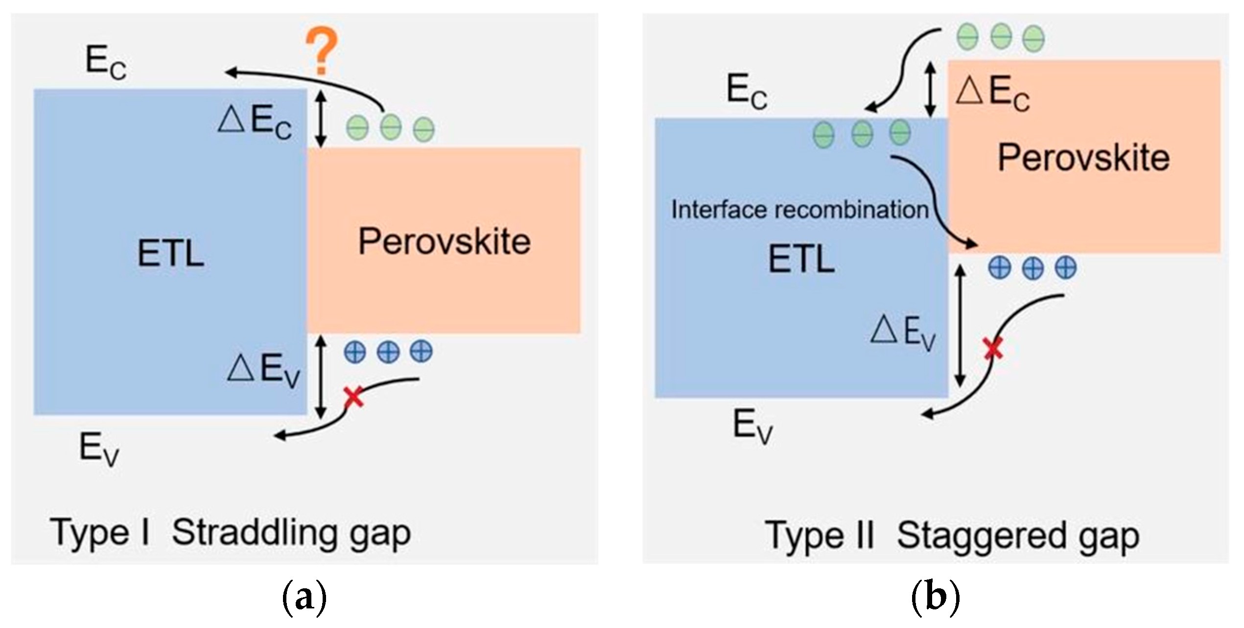
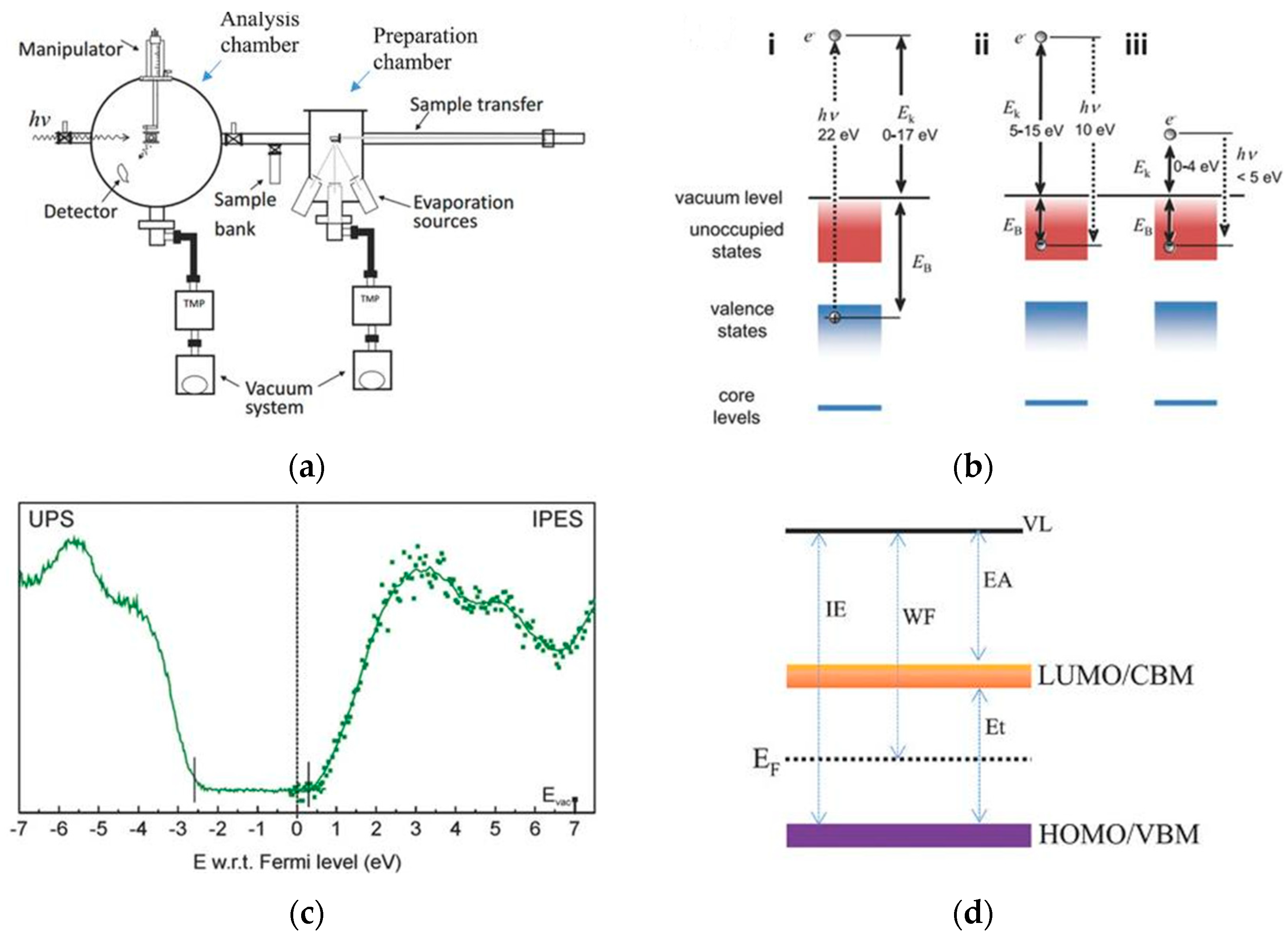
5. Formation Causes and Characterization Methods of Energy Level Misalignment

The alignment of interface energy bands has a crucial impact on the dynamic processes of carrier transport, extraction, and collection, and it can have the effect of suppressing charge accumulation, recombination, and reverse transport [52,96]. Figure 7 illustrates the interface and energy levels of the planar PSCs [28]. From the diagram, we can see that the PSCs have many interfaces in the structure of PSCs, including the ETL/perovskite interface (called ①), perovskite/HTL interface (called ②), cathode/ETL interface (called ③), and HTL/anode interface (called ④). These interfaces are critical, and the best charge extraction efficiency can be achieved when the energy offset at the interface is about 0.2 eV [97]. If the energy offset is too small, the weak built-in potential formed cannot efficiently extract the charges, resulting in charge accumulation and recombination on the interface; while if the energy offset is too large, energy spikes will be formed, which will hinder the extraction of carriers [98]. For buried interfaces, electron extraction and transfer are closely related to the ① and ③ arrangements of energy levels. In the process of electron extraction and transfer, electrons are transferred from the perovskite conduction band minimum (CBM) to ETL and then collected by the cathode. If there is no energy level barrier, this process can promote electron transport and increase electron mobility Meanwhile, it is important to minimize/prevent the transfer of unwanted holes at the interface; if not, undesirable recombination will occur at those interfaces. In general, the energy level alignment (ELA) on the interface decides the transfer/transport of charges and is also related to recombination at the interface; thus, device efficiency and stability are closely related to it. Therefore, the understanding of ELA at various interfaces is crucial for manufacturing efficient PSCs.
In general, the band arrangement is determined by the location of conduction and valence bands. Since we focus on the buried interface of the n-i-p structure, two common band arrangements at the ETL–perovskite interface are shown in Figure 8. When the Ec and Ev of the perovskite layer are both located inside the ETL, we call it a straddling gap (Figure 8a). When the Ec of the perovskite is higher than that of the ETL, for a type II staggered gap (Figure 8b), the amounts of conduction band shift (ΔEc) and valence band shift (ΔEv) are determined by the Ec and Ev differences between the electron transport layer and the perovskite layer. For ΔEv values, the ΔEv absolute value should be large enough to effectively extract electrons and block hole transfer, which requires the perovskite valence band to be far away from the ETL valence band, providing a high energy barrier for hole transfer. For ΔEc values, the situation is more complicated, and the Type II band arrangement is considered to be the best band arrangement in favor of the electron transport layer, but this is not absolute, because the holes in the perovskite Ev have the potential to bind with the electrons in the Ec of the ETL, resulting in interface recombination and Voc loss. This requires ΔEc values to be small enough to minimize interface recombination, and generally, we require ΔEc < 0.2 eV [99]. The potential barrier imposed by a positive ΔEc is why the type I band alignment is often regarded as unsuitable for current flow across the interface, but things do not always go this way. If the ETL is sufficiently thin (for example, <5 nm), then the tunneling effect may facilitate the flow of current across the interface [100,101]. The type I band alignment could reduce or stop interface recombination caused by the long distance in the ETL’s Ec and the perovskite’s Ev [102]. Energy level arrangement is very important for the extraction of charge carriers in perovskite solar cells, and different materials have different energy levels. Thus, to minimize the interface obstacles of charge carrier extraction, the following aspects should be considered when selecting charge transport materials: (1) wide band gap to minimize parasitic absorption; (2) appropriate energy levels, with the selective extraction of charge carriers; (3) high carrier mobility to reduce charge transport losses; (4) no loss path caused by defects to eliminate non-radiative recombination; (5) controlled interface coupling with perovskite to prevent cumulative charge loss.
In general, we think that the energy level arrangement between the perovskite layer, the electron transport layer, and the hole transport layer is the same as the arrangement in the vacuum. However, this assumption is only true if the layers are far enough apart from each other. Perovskite solar cells are layered structures, and there will inevitably be interface dipoles, band bending, and other phenomena. Band bending is usually caused by charge rearrangement at the interface. Unfavorable band bending affects the carrier transport at the interface and the device performance. For example, at the interface between the electron transport layer and the perovskite layer, the upward curved energy band can be regarded as an electron depletion region, forming a Schottky interface barrier that is not good for electron extraction and transport. It increases the non-radiative recombination center at the interface. If appropriate interface modifying is performed, then the energy band can be bent downward to form ohmic contact and reduce the interface barrier to promote electron transport. The corresponding effective hole collection can be achieved by bending up the energy band of the perovskite. In addition, large conduction band deviation leads to a high amount of carrier recombination at the interface, which affects the performance of the final device.
The work function is an important material parameter that characterizes the performance of devices by reflecting the size of the energy levels and electron and hole injection barriers at the contact interface of the conductor material. It is particularly sensitive to changes in material structure and composition, physical and chemical properties of the surface, and can be applied in the analysis of various surface properties. There are many methods for measuring the work function, which can be mainly classified into two categories: absolute measurement and relative measurement. Absolute measurement methods directly measure the work function, such as ultraviolet photoelectron spectroscopy (UPS), the electron beam blocking potential method, the field emission blocking potential method, and thermal electron emission. Relative measurement methods that indirectly measure the work function include Kelvin probe force microscopy (KPFM) and thermionic emission.
Ultraviolet photoelectron spectroscopy (UPS) and X-ray photoelectron spectroscopy (XPS) are commonly used techniques. Commonly used techniques include ultraviolet photoelectron spectroscopy (UPS) and X-ray photoelectron spectroscopy (XPS). UPS uses low-energy ultraviolet light as the excitation source to collect the outermost valence electrons of the sample. Figure 9a shows the schematic of the basic equipment used for UPS measurements. In the UPS measurements, UV or synchrotron radiation photons are used to measure the sample under ultra-high vacuum, and the kinetic energy (Ek) of the ejected electrons is measured. The binding energy (EB) of the electron from the valence band could be measured according to the conservation of energy (as illustrated in Figure 9b). The UPS analysis is able to provide an ionization potential (IE) and the highest occupied molecular orbital (HOMO) level of the film, which can be used to calculate the lowest unoccupied molecular orbital (LUMO) and its work function (WF) in combination with the optical band gap. XPS uses high-energy X-rays as the excitation source, which can detect inner-layer electrons of the sample and determine whether charge transfer or chemical reactions have occurred by changes in element binding energy. UPS can be combined with XPS to ensure charge transfer as well as the band bending at the interface [103,104].
UPS and XPS rely on photoelectrons to reflect the electronic structure information of the sample; thus, they can only characterize the levels of electronic energy in the occupied states of the sample, but they cannot provide information on the unoccupied states, such as the position of the conduction band minimum (CBM) of the sample. The sample CBM could be probed through inverse photoelectron spectroscopy (IPES), which provides the most direct measurement of the molecular LUMO. Electrons with kinetic energy Ek collide with the sample; meanwhile, the photons emitted by radiation transition to the unoccupied state are detected (as shown in sub-panel (ii) of Figure 9b), injecting a certain amount of energy into the electronic level of the unoccupied state of the sample, causing the sample to emit photons. Due to the analysis of photon energy, the electronic structure of the conduction band and the LUMO of the sample are obtained. By combining UPS and IPES, it is possible to determine the HOMO levels, LUMO levels, WF, as well as IE and to achieve the goal of studying interface properties, that is, ELA. Figure 9c illustrates typical UPS and IPES spectra [105], while Figure 9d illustrates the characterizations of the energy levels in this study.
Kelvin probe force microscopy (KPFM) is a surface electrical property analysis technique. KPFM is typically used in combination with atomic force microscopy (AFM) and the Kelvin method, and it has very high sensitivity. KPFM is mainly used to analyze the potential and work function changes of material surfaces, thus revealing the physical and chemical processes on the material surface. This method can be applied to study the interface potential distribution between P3HT: PCBM and inorganic solar cells [106,107,108]. KPFM has also been used in PSCs for the study of the local grain boundary [109], the distribution of the inner potential [110], and band diagrams [111]. Low energy inverse photoemission spectroscopy (LEIPS) uses electron energies of less than 4 eV (as illustrated in subpanel (iii) of Figure 9b), which are able to cut down the destruction of organic molecules [112,113,114].
Figure 9. (a) Layout of UPS measuring devices [28]. (b) Main schemes of experimental techniques for the determination of ionization potential and electron affinity: (i) UPS; (ii) IPES; (iii) low-energy inverse-photoemission spectroscopy (LEIPS) [112]. (c) An example of the combination of UPS and IPES to determine the HOMO and LUMO levels, respectively [105]. (d) Parameters for characterizing energy levels of materials in this work. VL: vacuum level; IE: ionization potential; WF: work function; EA: affinity energy; Et: transport gap [28].
Energies 16 05015 g009

6. Adjusting Energy-Level Alignment

As for solar cells, the energy level alignment significantly influences charge extraction, charge transfer, and charge recombination. The proper alignment of energy levels is essential for efficient solar cells. Miller et al. [103] investigated the location of the CH3N- H3PbI3 perovskite films on a variety of n-type (ZrO2, ZnO, and F: SnO2 (FTO)) substrates after solution deposition and various p-type (PEDOT: PSS, NiO, and Cu2O) substrates deposited on insulating substrates (Al2O3). It was found that the different characteristics of the substrate can change the band arrangement of the device. Kahn et al. [115] also made similar findings where perovskite was slightly p-type on NiOx substrates and n-type on TiO2 substrates (the VBM of NiOx and TiO2 are 0.7 and 1.4 eV, respectively). This shows that the underlying interface of perovskite can change the inherent properties of perovskite itself; therefore, utilizing a buried interface layer applied between the electron transport layer and that of perovskite can facilitate the transport and collection of charge carriers and can suppress interface charge recombination.
The reason why TiO2 has become a widely applied ETL in planar PSCs is that it possesses excellent optical transparency, easy fabrication, and high chemical stability. Nonetheless, its electron mobility is low, resulting in charge accumulation at the ETL/perovskite interface, which leads to reduced efficiency and hysteresis [116,117,118]. Li et al. [119] used a thin and dense TiO2/WO3 bilayer with high crystallinity, resulting in a sharp drop in leakage current, as shown in Figure 10a. In addition, in order to further illustrate the role of the WO3 layer in improving the energy level arrangement, UV photoemission spectroscopy (UPS) tests were conducted to determine the CBM and VBM of TiO2 and WO3, thus obtaining the energy level shown in Figure 10b. Compared to the original WO3/TiO2 bilayer, the WO3/TiO2 bilayer has a lower VBM, and the changed energy level structure can effectively block holes, thus reducing charge recombination. Li et al. [120] proposed a method for introducing a dopamine chelation-modified titanium dioxide surface treatment. Dopamine has a strong electron-donating ability and interfacial crosslinking ability, which is conducive to the direct injection of photogenerated electrons into the conduction band of TiO2 particles. Thus, effective charge transfer is realized and charge accumulation is reduced at the TiO2/perovskite interface. Ultraviolet photoelectron spectroscopy (UPS) analysis further confirmed this result, and dopamine-modified TiO2 has an ECB that is very close to the perovskite layer in energy (as shown in Figure 10c).
Compared to TiO2, SnO2 has advantages such as high electron mobility, low light loss, and preparation process in low temperatures [121,122,123]. Huang et al. [124] introduced a modified layer of dopamine (SAM) between SnO2 and the perovskite layer. Dopamine has a π-conjugated benzene structure that is conducive to electron transport. Self-assembled monolayers (SAMs) are also effective interface layers. The organic molecules for SAMs are usually composed of an anchoring group, a spacer, and a tail group. SAMs can provide the dipole moment in the interface, adjust the surface energy, and improve the affinity of the film or substrate, thereby optimizing the energy band alignment at the interface [125,126]. Yang et al. [127] modified the interface between SnO2 ETL and the perovskite layer, using 3-aminopropyltriethoxysilane (APTES) SAM as the interface layer (Figure 10d). The functional groups at the end of the APTES SAM formed a dipole on the SnO2 surface, causing the SnO2 work function to decrease and the built-in potential of the SnO2/perovskite heterojunction to increase (Figure 10e). The built-in potential not only suppresses the reverse transfer of electrons from SnO2 ETL to the peroxide layer but also helps to separate, transfer, and collect photogenerated carriers, thereby regulating the energy level alignment. Mu et al. [128] also used a SAM layer to anchor the SnO2 ETL. Using plant photosynthesis promoter choline chloride as the active agent, the surface defects of SnO2 were passivated; thus, the ETL was more similar to that of the perovskite. It has also been demonstrated that self-assembled monolayers (SAMs) can be used to fine tune the optical properties of the interface [125,129,130,131]. Because of their ionic properties, perovskite-type photovoltaic materials are prone to a variety of chemical interactions with different functional groups. Different surface chemistry or different chemical termination can significantly alter the electron density and energy level structure of the perovskite crystal surface. Yet, this effect is often overlooked. Zuo et al. [132] fixed SAMs with different end groups on SnO2 ETL, and the difference of the end functional groups resulted in different chemical interaction effects with perovskite film, as shown in Figure 10f,g. Surprisingly, the properties of PSCs run counter to the level alignment theory, suggesting that the chemical interaction is the main factor controlling the photoelectric properties of the interface. Similarly, the different spatial steric hindrance of chemical interactions resulting from different molecular structures is also the primary cause affecting the performance of the device. Chen used a series of C=O-functionalized adamantane derivatives to modify the SnO2/perovskite interface, and the electrostatic formula of each molecule is shown in Figure 10h. Due to the different distance between C=O and the massive adamantane ring, their steric hindrance is different, which affects the strength of chemical interaction and thus affects the passivation effect, and the effect on the energy level arrangement is shown in Figure 10i.
Figure 10. The effect of interface modification on the energy level of perovskites (a,b): interfacial charge transfer in TiO2/WO3 bilayer devices [119]. (c) Cell structure and corresponding energy levels of dopamine (DA)-coated TiO2 film [120]. (d) PSCs and the dipole moment distribution of SnO2 ETL modified by SAM. (e) Diagram with or without a SAM-modified SnO2/perovskite balance band, including depletion zone and built-in voltage [127]. (f) Perovskite solar cell device structure diagram and (g) charge dynamic diagram at the perovskite/SnO2 interface using different SAM-modified SnO2 (BA is benzoic acid, PA is 4-pyridinic acid, CBA is 4-cyano-benzoic acid, ABA is p-aminobenzoic acid, C13 is 3-propionic acid): ① photoluminescence process, ② PL quenching via trap states, ③ charge transfer process, ④ charge recombination via trap states, ⑤ power generation [20]. (h) Electrostatic potential ESP map of AD, ADCA, and ADAA molecules. Contact interfaces of SnO2 and perovskite planes with AA, AC, and AD, respectively, and (i) energy level diagram of device components [133].
Energies 16 05015 g010
The energy deviation of CBM in SnO2 film and CBM in perovskite film is reduced gradually with decreasing spatial hindrance, adjusting the effect of the interface band alignment, as shown in the figure. This indicates that larger hindrance impedes electron transfer, while smaller hindrance is favorable for electron transfer [133]. In general, inorganic salt ions, organic materials, and carbon materials can all effectively adjust the energy level arrangement. Due to the relatively unified test methods, some materials that adjust the energy level arrangement according to different material types are listed in Table 1 to provide the device architecture and key parameters.

7. Surface Defect Passivation

Many defects are found in the perovskite interface. Due to the inevitable use of organic/inorganic cations and annealing treatment during the preparation of perovskite films, the evaporation of organic/inorganic cations will form vacancy defects, and the halide ions will migrate. This also leaves deep level defects caused by undercoordinated Pb2+ and shallow level defects caused by iodine vacancies [148,149,150]. In particular, these deep traps will cause severe Shockley-Read-Hall non-radiative recombination, significantly impeding the extraction of interface charges. With the commonly used SnO2 ETL, under-coordinated Sn and oxygen vacancies (Vo) as well as surface hydroxyl groups [151,152] are generated on the surface. Other metal oxide ETLs, for example, ZnO, TiO2, and NiOx, have similar defects. Compared to the n-i-p planar structure, the mesoporous structure contains additional mesoporous scaffoldings to shorten the electron transport distance and facilitate electron extraction to reduce the recombination rate. However, the mesoporous structure requires high-temperature sintering, which will increase energy consumption and limit its use in flexible substrates and large-scale manufacturing. After decades of development, PSCs gradually changed from a porous structure to a planar structure. However, the low-temperature treated electron transport layer inevitably faces the problems of imperfect interface and charge recombination between the perovskite layer and perovskite layer. Therefore, the buried interface engineering to perfect the interface has been paid much attention and studied, and it is believed that the defects can be reduced by the passivation of the interface materials. We also focus on the buried interface passivation of planar structure perovskite solar cells.
Tan et al. [153] prepared TiO2-Cl colloidal nanocrystals with chlorine-capped ends, which were used to passivate the ETL/perovskite interface in conventional PSCs. DFT calculations showed that the Cl at the interface resulted in a stronger binding between TiO2 and the perovskite, and the Pb-I antisite defects on the surface of the PbI2-terminated perovskite induced localized states close to the valence band edge. By comparison, the Pb-Cl antisite defects on the surface of the PbCl2-terminated perovskite are hard to form (Figure 11a). Li et al. [154] similarly prepared ETLs containing Cl, significantly reducing the defect density and enhancing the carrier mobility, which significantly reduced the interface recombination and charge extraction losses. Bu et al. [155] introduced K+ ions into SnO2 ETLs through potassium treatment (Figure 11b), which can undergo substitution reaction with surface Br ions of the perovskite film to form the strong ionic bonding of KBr, passivating the halide vacancies at the interface. A single K+ and Cl could just passivate one charged defect. Liu et al. [156] used inorganic binary alkaline halide KX, where X is a halide, to passivate two types of charged defects by fully utilizing both K+ cation and Cl anion. Zhu et al. [157] used the SnO2-KCl compound as an ETL to passivate the defects at the bottom contact of the ETL/perovskite interface, resulting in the enhancement of the steady-state photoluminescence (PL) as well as time-resolved photoluminescence (TRPL) intensities (Figure 11c), demonstrating the suppression of non-radiative recombination of the perovskite film on SnO2-KCl. Besides Cl, other halide anions (Br, F, I) also have passivation effects [143,158]. Wang et al. [159] modified SnO2 with CsF containing strongly electronegative F ions and performed XPS tests on the surface with or without CsF-SnO2 (Figure 11d). The presence of characteristic peaks at 685.2 eV in the XPS diagram of F1s indicated the formation of an Sn-F bond, and all O1s peaks were reversed-rolled into two peaks. The presence of two characteristic peaks at 530.5 eV and 532.2 indicated the existence of lattice oxygen and hydroxyl on the surface of SnO2. When CsF was added, the hydroxyl group strength decreased obviously. This can be attributed to the fact that the F atom can bind to the undercoordinated Sn to form chemical doping. The F ion can also contribute to better carrier collection by bonding/substituting the formed hydroxyl group. There are two types of hydroxyl groups: terminal hydroxyl (OHT) that is bound to a metal site with basic characteristics, and bridging hydroxyl (OHB) that is bound to two metal sites with acidic characteristics [160]. Jung et al. [145] used NH4F for surface treatment, and the weakly acidic ammonium cation from NH4F reacted with OHT on the SnO2 surface, while the fluoride anion replaced the defect position (as shown in Figure 11e).
These inorganic molecules, when used as buried interface materials with a single functional group, have relatively simple functions. However, materials containing both cations and anions can achieve multiple chemical bonds (such as ionic bonds, coordination bonds, and hydrogen bonds) with perovskite and SnO2 layers, thus simultaneously passivating traps with positive and negative charges. Gong et al. [161] used KFSI with functional groups containing F, K+, and S=O to passivate buried interfaces. F can form hydrogen bonds with organic cations, while it can form coordination bonds with Pb2+ and Sn4+. The S=O functional group can form coordination bonds with Pb2+ and Sn4+. The synergistic effect of multiple chemical bonds, such as hydrogen bonds, coordination bonds, and ionic bonds, resulted in an efficiency of 24.17%, and the same passivation effect was confirmed [162]. When TiO2 is used as an ETL, the S=O functional group also has a passivating effect. -SO3 can interact with Ti4+ and connect with TiO2, significantly reducing oxygen vacancy [163]. Liu et al. [164] proposed the use of 4-trifluoromethylphenyl iodide ammonium (CF3PhAI), composed of organic cations (C7H7NF3+) and inorganic anions (I), as the passivator for defects. When CF3PhAI is introduced in SnO2 and perovskite, it can chemically connect with SnO2 through Lewis coordination as well as electrostatic coupling, significantly passivating the coordination-deficient Sn and filling oxygen vacancies. The synergistic effect of the trifluoromethyl (-CF3), -NH3+, and I functional groups in CF3PhAI is essential to increase efficiency and stability. The PCE of the fabricated target device was 23.06%, while the PCE of the control sample was 19.85%. Aminothiourea (ADT) with functional groups is also used as a multifunctional modifier to enhance the interface of SnO2/perovskite. The areas with low electronic density are located on the -C=NH and -C=S sides. In ADT, N, and S atoms have lone pairs of electrons. -NH2 could also be connected to the perovskite side through the act of forming hydrogen bonds with -NH2. The ADT and perovskite/SnO2 coordinate bond enhances the interface connection, decreases the non-radiative recombination, and speeds up the extraction and transfer efficiency [165]. -COOH could fill the oxygen vacancies in the ETL by reacting with -OH on the SnO2 surface as well as coordinating with under-coordinated Sn4+ bonds, as widely verified [166,167]. The passivation of interface defects by Cl has also been widely confirmed [168,169]. Yi et al. [170] deposited Ce2(SO4)3 material on the surface of SnO2 by spin coating. The synergistic effect of Ce3+ and SO42− reduces the number of dangling Sn bonds in the perovskite layer, with the reduction in the proportion of Sn2+, and Ce3+ being beneficial to the reduction of I0 defects. Gao et al. [171] used porous organic cages (POCs) with internal cavities and weak interactions between molecules to passivate the buried interface. On the one hand, POCs are rich in function groups, which provide many chelating sites for the chemical bonding of SnO2 and perovskite, stitching the embedded interfaces together to realize spontaneous recombination. Thus, multiple dentate chelation is used to control all kinds of defects at the surface. Additionally, the host and guest interaction between POCs could effectively trap iodine ions and prevent the migration of iodine ions to the embedded interface and ITO. This is also the first application of POCs as PSCs interface function materials.
Numerous studies have demonstrated the ability of different functional groups to passivate interface defects. However, in addition to chemical interactions, ion configuration, steric hindrance, and other factors can also affect passivation ability. Zhang et al. [172] researched the influence of different anion configurations on the FAPbI3/SnO2 interface. They studied lithium salts of three anions (CO32−, C2O42−, and HCOO-) to gain insight into the origins of the interactions between these anions and perovskites. First-principle calculations were carried out within the DFT framework, revealing that CO32−, C2O42−, and HCOO ions have stronger affinity to FA+ than Pb2+ because their adsorption energies are more negative than those of the latter. The binding between these anions and FA+ is due to the fact that hydrogen bonds between N-H and C=O and CO32− can generate stronger hydrogen bonds with FA+ than the other two anions. Furthermore, the formation energy of FA+ vacancies increases after the addition of anions, indicating that they can passivate FA+ defects. Among the three anions, CO32− is more effective at passivating FA+ defects, which is related to the configuration of the C-O and C=O groups.

8. Modulating Morphology

The performance of PSCs is largely influenced by the morphology of perovskite films. Thus, the development of methods to improve the quality of the films is a key issue for PSCs. Currently, studies have confirmed that high-phase purity and crystallinity, as well as even and fewer grain boundaries, can significantly promote the performance as well as the stability of the devices [173,174,175,176,177]. The nucleation of halide perovskite crystals in the precursor is uneven, affected by is supersaturation, impurities, and substrates [178]. Among them, the substrate has remarkable influence on perovskite formation, such as the substrate’s chemical properties, morphology, temperature [171,179,180], and other factors. Therefore, a good perovskite epitaxial substrate is the basis for obtaining high-quality perovskite thin films. The buried interface can affect the subsequent perovskite nucleation growth by improving the wettability of the charge transport layer and regulating the morphology of residual PbI2. This can increase the grain size of perovskite and improve the crystallinity to reduce the non-radiation loss caused by the existence of defects at the grain boundary. In addition, the buried interface can also reduce the interfacial strain between the growing perovskite grains and the electron transport layer by passivating the defects at the interface and acting as the nucleation site to improve the carrier transport at the interface. Moreover, the stability of the device is improved by reducing the lattice distortion of perovskite grains [181,182,183,184].
It is well known that lead iodide-based perovskite-type materials degrade to PbI2 in some conditions, which is obviously detrimental to the decomposition of perovskite layers [185]. However, previous studies have shown that a moderate amount of PbI2 can shape a thin layer of PbI2 at the crystal surface, reducing GBs and surface recombination, preventing electron transfer, and improving carrier behavior [186,187,188]. Nevertheless, residual PbI2 in perovskite films can photodegrade and generate holes, which will affect long-term stability [189,190]. Therefore, Deng et al. [191] used 4,4′-diaminodiphenyl derivatives as passivators to modify SnO2 and to regulate the distribution and morphology of PbI2. The original perovskite film has residual PbI2 crystalline blocks randomly distributed at the perovskite crystal boundary and surface. After adding a buried interface modification agent, the residual PbI2 can be rearranged to form nanosheets and can be evenly distributed at the surface of particles. The structure of the perovskite film and its top-view scanning electron microscopy (SEM) are shown in Figure 12a. Adding a buried interface modification agent is conducive to the crystallization, making the perovskite film dense and the grain size larger. More reports have studied the surface morphology of PbI2 deposited on the buried interface as well as the effect on the subsequent growth of perovskite films. Sun et al. [192] introduced nickel acetate NiAc2 on the buried interface, and the Ac evaporated upwards through the PbI2 layer, causing the PbI2 layer to form a porous shape. The resulting perovskite film formed has less unreacted and residual PbI2 on the grain boundary (Figure 12b), and cross sectional SEM imaging further verifies that some unreacted PbI2 can be clearly seen on the top or bottom of the perovskite film. In contrast, there are no obvious PbI2 crystals in the perovskite film deposited on NiAc2-modified SnO2 ETL. Zhang et al. [193] proposed that the perovskite film deposited on a smooth and uniform PbI2 film is smoother, is denser, and has a uniform distribution of grain size and no pinholes, as shown in Figure 12c. In addition, other studies have also reduced the amount of PbI2 in the perovskite film by decreasing the ETL surface roughness (Figure 12d,e) [189,194,195].
Due to the mismatched coefficient between the base material and the perovskite, severe lattice strain can be induced. As shown in Figure 13a, a strain is produced in the perovskite film during cooling [196]. When the perovskite is cooled from a temperature greater than 100 °C to room temperature, it is likely to shrink because of its thermal expansion coefficient. While the perovskite film is deposited on the substrate with a less thermal expansion coefficient, the perovskite is unable to shrink, which leads to tensile strain in the plane direction. In order to compensate for the reduced lateral contraction in the cooling process, the membrane contracts more in the out-of-plane direction, causing compression strain in that direction [197,198]. Wang et al. [159] studied the influence of interface stress on the layer of CsF and made a grazing incidence X-ray diffraction (GIXRD) measurement. For the original SnO2 sample, as the incident angle (ω) increased, the diffraction peak shifted to lower angles (Figure 13b). Based on Bragg’s equation (2dsinθ ¼ nλ), this phenomenon shows lattice expansion, which shows the existence of tensile strain along the plane. The Williamson-Hall plot shows that adding CsF can effectively alleviate the strain at the SnO2/perovskite interface, which is important for perovskite growth at the interface. Zhang et al. [199] found that a protonated aminosilane coupling agent (PASCA-Br) modified (3-aminopropyl) triethoxysilane (APTES) can alleviate strain stress (Figure 13c,d), where the branched alkyl bromide ammonium terminal is a well-matched growth site for perovskite, reducing lattice distortion and the resulting interface strain. In addition, the R-NH3Br end will form a strong chemical bond with the undercoordinated Pb atoms, greatly reducing lattice distortion. Materials such as diethanolamine (DEA) [200], 2,2′-(perfluoronaphthalene-2,6-diylidene) dimalononitrile (F6TCNNQ) [201], dopamine [120], etc., can also reduce interface stress.
Surface wettability at the interface between perovskite film and its substrate can influence the nucleation and growth of the succeeding grain, which is the basis for forming high-quality perovskite films. In a study conducted by Sajjad Ahmad [202], they investigated the interaction of ABABr (4-(2-aminoethyl) benzoic acid bromide) with NiOx and different perovskite layers were studied, and they measured the water contact angle. After modification, the reduced contact angle is able to release surface tension, which is beneficial for the form diffusion of the precursor as well as the formation of grains. The perovskite particles become denser and more enlarged without any pinholes. Wei et al. [203] improved the density and wettability of SnO2 layers using polyethylene glycol (PEG). Furthermore, the PN4N middle layer can be used to improve the surface wettability so that a high-quality perovskite film can be formed [171]. Red carbon quantum dots (RCQs) can effectively bind the incompletely coordinated Pb2+ in perovskite, enhancing hydrophilicity, increasing the hydrophilicity, reducing the Gibbs free energy, and promoting of high-quality films [204].

9. Summary and Outlook

In summary, the role and mechanism of the buried interface in defect passivation, energy level regulation, and shape control are summarized, and the latest progress in interface engineering in these aspects is reviewed. Research shows that the buried engineering effectively passivates the ETL/perovskite defects and regulates the energy level arrangement as well as the charge extraction at the interface, and it improves the quality of perovskite film. This improvement can enhance PCE and the stability of PSCs. By adjusting the structure of the modified material and the steric hindrance of the functional groups, the interface defects can be effectively passivated, and the non-radiative bonding loss of the interface can be reduced. The energy level arrangement at the interface significantly affects the carrier transport process, and the buried interface engineering can adjust the energy level to promote the interface charge extraction. In addition, the buried interface modification strategy can improve the morphological quality of perovskite film by improving the wettability and adjusting the coefficient of thermal expansion. Thus, the buried interface can improve the PCE and stability of perovskite solar cells from multiple dimensions, which is a simple and effective optimization strategy.
The mechanism of interface modification and the selection of materials need to be further studied in order to achieve defect passivation, to optimize energy level arrangement, and to improve morphology. In addition, more advanced and efficient characterization methods are needed to further study the properties of buried interfaces in order to expand its application. The interface engineering should also adapt to the commercial large-scale production mode and play a maximum role.

Author Contributions

Conceptualization, H.S., Y.P., C.L., M.G., L.L. and H.F.; investigation, Y.P. and C.L.; resources, H.S., M.G. and L.L.; data curation, Y.P. and C.L.; writing—original draft preparation, Y.P. and C.L.; writing—review and editing, Y.P., C.L., H.S. and M.G. All authors have read and agreed to the published version of the manuscript.

Funding

This work was supported by the Guangdong Basic and Applied Basic Research Foundation (2021B1515120028), National Natural Science Foundation of China (52130204, 52174376, 51971174), Joint Research Funds of the Department of Science and Technology of Shaanxi Province and NPU (2020GXLH-Z-024), Science and Technology Innovation Team Plan of Shaan Xi Province (2021TD-17), The Youth Innovation Team of Shaanxi Universities, Natural Science Basic Research Plan in Shaanxi Province of China (2020JQ-144), and Fundamental Research Funds for the Central Universities (D5000210902).

Data Availability Statement

Research data are not shared.

Conflicts of Interest

The authors declare no conflict of interest.

References

  1. Jeon, N.J.; Noh, J.H.; Yang, W.S.; Kim, Y.C.; Ryu, S.; Seo, J.; Seok, S.I. Compositional engineering of perovskite materials for high-performance solar cells. Nature 2015, 517, 476–480. [Google Scholar] [CrossRef] [PubMed]
  2. Wehrenfennig, C.; Eperon, G.E.; Johnston, M.B.; Snaith, H.J.; Herz, L.M. High charge carrier mobilities and lifetimes in organolead trihalide perovskites. Adv. Mater. 2014, 26, 1584–1589. [Google Scholar] [CrossRef] [PubMed] [Green Version]
  3. Xiao, Z.; Dong, Q.; Bi, C.; Shao, Y.; Yuan, Y.; Huang, J. Solvent annealing of perovskite-induced crystal growth for photovoltaic-device efficiency enhancement. Adv. Mater. 2014, 26, 6503–6509. [Google Scholar] [CrossRef] [PubMed]
  4. Miyata, A.; Mitioglu, A.; Plochocka, P.; Portugall, O.; Wang, J.T.-W.; Stranks, S.D.; Snaith, H.J.; Nicholas, R.J. Direct measurement of the exciton binding energy and effective masses for charge carriers in organic–inorganic tri-halide perovskites. Nat. Phys. 2015, 11, 582–587. [Google Scholar] [CrossRef] [Green Version]
  5. Kojima, A.; Teshima, K.; Shirai, Y.; Miyasaka, T. Organometal Halide Perovskites as Visible-Light Sensitizers for Photovoltaic Cells. J. Am. Chem. Soc. 2009, 131, 6050. [Google Scholar] [CrossRef]
  6. NREL Best Research-Cell Efficiencies. Available online: https://www.nrel.gov/pv/assets/pdfs/best-research-cell-efficiencies-rev220630.pdf (accessed on 20 October 2022).
  7. Isikgor, F.H.; Zhumagali, S.; Merino, L.V.T.; De Bastiani, M.; McCulloch, I.; De Wolf, S. Molecular engineering of contact interfaces for high-performance perovskite solar cells. Nat. Rev. Mater. 2022, 8, 89–108. [Google Scholar] [CrossRef]
  8. Correa-Baena, J.-P.; Saliba, M.; Buonassisi, T.; Gratzel, M.; Abate, A.; Tress, W.; Hagfeldt, A. Promises and challenges of perovskite solar cells. Science 2017, 358, 739–744. [Google Scholar] [CrossRef] [Green Version]
  9. Park, N.-G.; Segawa, H. Research Direction toward Theoretical Efficiency in Perovskite Solar Cells. ACS Photonics 2018, 5, 2970–2977. [Google Scholar] [CrossRef]
  10. Xiang, W.; Liu, S.F.; Tress, W. Interfaces and Interfacial Layers in Inorganic Perovskite Solar Cells. Angew. Chem. Int. Ed. Engl. 2021, 60, 26440–26453. [Google Scholar] [CrossRef]
  11. Luo, D.; Li, X.; Dumont, A.; Yu, H.; Lu, Z.H. Recent Progress on Perovskite Surfaces and Interfaces in Optoelectronic Devices. Adv. Mater. 2021, 33, e2006004. [Google Scholar] [CrossRef]
  12. Chen, H.; Chen, Y.; Zhang, T.; Liu, X.; Wang, X.; Zhao, Y. Advances to High-Performance Black-Phase FAPbI3 Perovskite for Efficient and Stable Photovoltaics. Small Struct. 2021, 2, 2000130. [Google Scholar] [CrossRef]
  13. Wang, Y.; Wu, T.; Barbaud, J.; Kong, W.; Cui, D.; Chen, H.; Yang, X.; Han, L. Stabilizing heterostructures of soft perovskite semiconductors. Science 2019, 365, 687–691. [Google Scholar] [CrossRef] [PubMed]
  14. Jiang, Q.; Zhao, Y.; Zhang, X.; Yang, X.; Chen, Y.; Chu, Z.; Ye, Q.; Li, X.; Yin, Z.; You, J. Surface passivation of perovskite film for efficient solar cells. Nat. Photonics 2019, 13, 460–466. [Google Scholar] [CrossRef]
  15. Li, Z.; Wu, M.; Yang, L.; Guo, K.; Duan, Y.; Li, Y.; He, K.; Xing, Y.; Zhang, Z.; Zhou, H.; et al. 24.64%-Efficiency MA-Free Perovskite Solar Cell with Voc of 1.19 V Enabled by a Hinge-Type Fluorine-Rich Complex. Adv. Funct. Mater. 2023, 33, 2212606. [Google Scholar] [CrossRef]
  16. Zhu, X.; Du, M.; Feng, J.; Wang, H.; Xu, Z.; Wang, L.; Zuo, S.; Wang, C.; Wang, Z.; Zhang, C.; et al. High-Efficiency Perovskite Solar Cells with Imidazolium-Based Ionic Liquid for Surface Passivation and Charge Transport. Angew. Chem. Int. Ed. Engl. 2021, 60, 4238–4244. [Google Scholar] [CrossRef] [PubMed]
  17. Chen, S.; Dai, X.; Xu, S.; Jiao, H.; Zhao, L.; Huang, J. Stabilizing perovskite-substrate interfaces for high-performance perovskite modules. Science 2021, 373, 902–907. [Google Scholar] [CrossRef]
  18. Yang, X.; Luo, D.; Xiang, Y.; Zhao, L.; Anaya, M.; Shen, Y.; Wu, J.; Yang, W.; Chiang, Y.H.; Tu, Y.; et al. Buried Interfaces in Halide Perovskite Photovoltaics. Adv. Mater. 2021, 33, e2006435. [Google Scholar] [CrossRef]
  19. Yang, Y.; Yang, M.; Moore, D.T.; Yan, Y.; Miller, E.M.; Zhu, K.; Beard, M.C. Top and bottom surfaces limit carrier lifetime in lead iodide perovskite films. Nat. Energy 2017, 2, 16207. [Google Scholar] [CrossRef]
  20. Yang, B.; Suo, J.; Di Giacomo, F.; Olthof, S.; Bogachuk, D.; Kim, Y.; Sun, X.; Wagner, L.; Fu, F.; Zakeeruddin, S.M.; et al. Interfacial Passivation Engineering of Perovskite Solar Cells with Fill Factor over 82% and Outstanding Operational Stability on n-i-p Architecture. ACS Energy Lett. 2021, 6, 3916–3923. [Google Scholar] [CrossRef]
  21. Saparov, B.; Mitzi, D.B. Organic-Inorganic Perovskites: Structural Versatility for Functional Materials Design. Chem. Rev. 2016, 116, 4558–4596. [Google Scholar] [CrossRef]
  22. Saliba, M.; Correa-Baena, J.P.; Gratzel, M.; Hagfeldt, A.; Abate, A. Perovskite Solar Cells: From the Atomic Level to Film Quality and Device Performance. Angew Chem. Int. Ed. Engl. 2018, 57, 2554–2569. [Google Scholar] [CrossRef] [PubMed]
  23. Goldschmidt, V.M. Die Gesetze der Krystallochemie. Naturwissenschaften 1926, 14, 477–485. [Google Scholar] [CrossRef]
  24. Choi, K.; Choi, H.; Min, J.; Kim, T.; Kim, D.; Son, S.Y.; Kim, G.-W.; Choi, J.; Park, T. A Short Review on Interface Engineering of Perovskite Solar Cells: A Self-Assembled Monolayer and Its Roles. Sol. RRL 2019, 4, 1900251. [Google Scholar] [CrossRef]
  25. Lin, X.; Cui, D.; Luo, X.; Zhang, C.; Han, Q.; Wang, Y.; Han, L. Efficiency progress of inverted perovskite solar cells. Energy Environ. Sci. 2020, 13, 3823–3847. [Google Scholar] [CrossRef]
  26. Wu, P.; Wang, S.; Li, X.; Zhang, F. Advances in SnO2-based perovskite solar cells: From preparation to photovoltaic applications. J. Mater. Chem. A 2021, 9, 19554–19588. [Google Scholar] [CrossRef]
  27. You, J.; Meng, L.; Song, T.B.; Guo, T.F.; Yang, Y.M.; Chang, W.H.; Hong, Z.; Chen, H.; Zhou, H.; Chen, Q.; et al. Improved air stability of perovskite solar cells via solution-processed metal oxide transport layers. Nat. Nanotechnol. 2016, 11, 75–81. [Google Scholar] [CrossRef]
  28. Wang, S.; Sakurai, T.; Wen, W.; Qi, Y. Energy Level Alignment at Interfaces in Metal Halide Perovskite Solar Cells. Adv. Mater. Interfaces 2018, 5, 1800260. [Google Scholar] [CrossRef]
  29. Yang, Z.; Dou, J.; Wang, M. Interface Engineering in n-i-p Metal Halide Perovskite Solar Cells. Sol. RRL 2018, 2, 1800177. [Google Scholar] [CrossRef]
  30. Shi, J.; Li, Y.; Li, Y.; Li, D.; Luo, Y.; Wu, H.; Meng, Q. From Ultrafast to Ultraslow: Charge-Carrier Dynamics of Perovskite Solar Cells. Joule 2018, 2, 879–901. [Google Scholar] [CrossRef] [Green Version]
  31. Ponseca, C.S.J.; Savenije, T.J.; Abdellah, M.; Zheng, K.; Yartsev, A.; Pascher, T.; Harlang, T.; Chabera, P.; Pullerits, T.; Stepanov, A.; et al. Organometal halide perovskite solar cell materials rationalized: Ultrafast charge generation, high and microsecond-long balanced mobilities, and slow recombination. J. Am. Chem. Soc. 2014, 136, 5189–5192. [Google Scholar] [CrossRef]
  32. Sum, T.C.; Mathews, N.; Xing, G.; Lim, S.S.; Chong, W.K.; Giovanni, D.; Dewi, H.A. Spectral Features and Charge Dynamics of Lead Halide Perovskites: Origins and Interpretations. Acc. Chem. Res. 2016, 49, 294–302. [Google Scholar] [CrossRef]
  33. Frenkel, J. On the Transformation of Light into Heat in Solids. II. Phys. Rev. 1931, 37, 1276–1294. [Google Scholar] [CrossRef]
  34. Wannier, G.H. The Structure of Electronic Excitation Levels in Insulating Crystals. Phys. Rev. 1937, 52, 191–197. [Google Scholar] [CrossRef]
  35. Elliott, R.J. Intensity of Optical Absorption by Excitons. Phys. Rev. 1957, 108, 1384–1389. [Google Scholar] [CrossRef]
  36. Fang, H.; Li, X.; Zhou, Y.; Sun, H. Ultrafast Spectroscopy of Hot Carriers in Perovskites. Acta Opt. Sin. 2021, 41, 0823009. [Google Scholar] [CrossRef]
  37. Shockley, W.; Queisser, H.J. Detailed Balance Limit of Efficiency of p-n Junction Solar Cells. J. Appl. Phys. 1961, 32, 510–519. [Google Scholar] [CrossRef]
  38. Xing, G.; Mathews, N.; Sun, S.; Lim, S.S.; Lam, Y.M.; Graetzel, M.; Mhaisalkar, S.; Sum, T.C. Long-Range Balanced Electron- and Hole-Transport Lengths in Organic-Inorganic CH3NH3PbI3. Science 2013, 342, 344–347. [Google Scholar] [CrossRef]
  39. Stranks, S.D.; Eperon, G.E.; Grancini, G.; Menelaou, C.; Alcocer, M.J.P.; Leijtens, T.; Herz, L.M.; Petrozza, A.; Snaith, H.J. Electron-Hole Diffusion Lengths Exceeding 1 Micrometer in an Organometal Trihalide Perovskite Absorber. Science 2013, 342, 341–344. [Google Scholar] [CrossRef] [Green Version]
  40. Hegedus, S.; Luque, A. Handbook of Photovoltaic Science and Engineering; John Wiley & Sons: Hoboken, NJ, USA, 2011. [Google Scholar]
  41. Sze, S.M.; Li, Y.; Ng, K.K. Physics of Semiconductor Devices; John Wiley & Sons: Hoboken, NJ, USA, 2021. [Google Scholar]
  42. Chen, J.; Park, N.G. Causes and Solutions of Recombination in Perovskite Solar Cells. Adv. Mater. 2019, 31, e1803019. [Google Scholar] [CrossRef]
  43. Luo, D.; Su, R.; Zhang, W.; Gong, Q.; Zhu, R. Minimizing non-radiative recombination losses in perovskite solar cells. Nat. Rev. Mater. 2019, 5, 44–60. [Google Scholar] [CrossRef]
  44. Ball, J.M.; Petrozza, A. Defects in perovskite-halides and their effects in solar cells. Nat. Energy 2016, 1, 16149. [Google Scholar] [CrossRef]
  45. Huang, J.; Yuan, Y.; Shao, Y.; Yan, Y. Understanding the physical properties of hybrid perovskites for photovoltaic applications. Nat. Rev. Mater. 2017, 2, 17042. [Google Scholar] [CrossRef]
  46. Aranda, C.; Guerrero, A.; Bisquert, J. Ionic Effect Enhances Light Emission and the Photovoltage of Methylammonium Lead Bromide Perovskite Solar Cells by Reduced Surface Recombination. ACS Energy Lett. 2019, 4, 741–746. [Google Scholar] [CrossRef]
  47. Yang, D.; Zhang, X.; Wang, K.; Wu, C.; Yang, R.; Hou, Y.; Jiang, Y.; Liu, S.; Priya, S. Stable Efficiency Exceeding 20.6% for Inverted Perovskite Solar Cells through Polymer-Optimized PCBM Electron-Transport Layers. Nano Lett. 2019, 19, 3313–3320. [Google Scholar] [CrossRef] [PubMed]
  48. Abdi-Jalebi, M.; Dar, M.I.; Senanayak, S.P.; Sadhanala, A.; Andaji-Garmaroudi, Z.; Pazos-Outon, L.M.; Richter, J.M.; Pearson, A.J.; Sirringhaus, H.; Graetzel, M.; et al. Charge extraction via graded doping of hole transport layers gives highly luminescent and stable metal halide perovskite devices. Sci. Adv. 2019, 5, eaav2012. [Google Scholar] [CrossRef] [PubMed] [Green Version]
  49. Arora, N.; Dar, M.I.; Hinderhofer, A.; Pellet, N.; Schreiber, F.; Zakeeruddin, S.M.; Graetzel, M. Perovskite solar cells with CuSCN hole extraction layers yield stabilized efficiencies greater than 20%. Science 2017, 358, 768–771. [Google Scholar] [CrossRef] [PubMed] [Green Version]
  50. Wang, S.; Zhu, Y.; Sun, W.; Miao, X.; Ma, Z.; Yang, C.; Liu, B.; Li, S.; Ma, R.; Wang, C. Large guanidinium cation enhance photovoltage for perovskite solar cells via solution-processed secondary growth technique. Sol. Energy 2018, 176, 118–125. [Google Scholar] [CrossRef]
  51. Tress, W.; Yavari, M.; Domanski, K.; Yadav, P.; Niesen, B.; Correa Baena, J.P.; Hagfeldt, A.; Graetzel, M. Interpretation and evolution of open-circuit voltage, recombination, ideality factor and subgap defect states during reversible light-soaking and irreversible degradation of perovskite solar cells. Energy Environ. Sci. 2018, 11, 151–165. [Google Scholar] [CrossRef]
  52. Wolff, C.M.; Zu, F.; Paulke, A.; Toro, L.P.; Koch, N.; Neher, D. Reduced Interface-Mediated Recombination for High Open-Circuit Voltages in CH3NH3PbI3 Solar Cells. Adv. Mater. 2017, 29, 1700159. [Google Scholar] [CrossRef]
  53. Chen, J.; Sheng, Y.; Ko, S.; Liu, L.; Han, H.; Li, X. Push–pull porphyrins with different anchoring group orientations for fully printable monolithic dye-sensitized solar cells with mesoscopic carbon counter electrodes. New J. Chem. 2015, 39, 5231–5239. [Google Scholar] [CrossRef]
  54. Rajagopal, A.; Yao, K.; Jen, A.K. Toward Perovskite Solar Cell Commercialization: A Perspective and Research Roadmap Based on Interfacial Engineering. Adv. Mater. 2018, 30, e1800455. [Google Scholar] [CrossRef] [PubMed]
  55. Wang, H.; Guerrero, A.; Bou, A.; Al-Mayouf, A.M.; Bisquert, J. Kinetic and material properties of interfaces governing slow response and long timescale phenomena in perovskite solar cells. Energy Environ. Sci. 2019, 12, 2054–2079. [Google Scholar] [CrossRef]
  56. Weber, S.A.L.; Hermes, I.M.; Turren-Cruz, S.-H.; Gort, C.; Bergmann, V.W.; Gilson, L.; Hagfeldt, A.; Graetzel, M.; Tress, W.; Berger, R. How the formation of interfacial charge causes hysteresis in perovskite solar cells. Energy Environ. Sci. 2018, 11, 2404–2413. [Google Scholar] [CrossRef] [Green Version]
  57. Shi, J.; Li, D.; Luo, Y.; Wu, H.; Meng, Q. Opto-electro-modulated transient photovoltage and photocurrent system for investigation of charge transport and recombination in solar cells. Rev. Sci. Instrum. 2016, 87, 123107. [Google Scholar] [CrossRef] [PubMed] [Green Version]
  58. Yoo, J.J.; Wieghold, S.; Sponseller, M.C.; Chua, M.R.; Bertram, S.N.; Hartono, N.T.P.; Tresback, J.S.; Hansen, E.C.; Correa-Baena, J.-P.; Bulović, V.; et al. An interface stabilized perovskite solar cell with high stabilized efficiency and low voltage loss. Energy Environ. Sci. 2019, 12, 2192–2199. [Google Scholar] [CrossRef] [Green Version]
  59. Jung, E.H.; Jeon, N.J.; Park, E.Y.; Moon, C.S.; Shin, T.J.; Yang, T.Y.; Noh, J.H.; Seo, J. Efficient, stable and scalable perovskite solar cells using poly(3-hexylthiophene). Nature 2019, 567, 511–515. [Google Scholar] [CrossRef]
  60. Deng, J.; Zhang, H.; Wei, K.; Xiao, Y.; Zhang, C.; Yang, L.; Zhang, X.; Wu, D.; Yang, Y.; Zhang, J. Molecular Bridge Assisted Bifacial Defect Healing Enables Low Energy Loss for Efficient and Stable Perovskite Solar Cells. Adv. Funct. Mater. 2022, 32, 2209516. [Google Scholar] [CrossRef]
  61. Ni, Z.; Bao, C.; Liu, Y.; Jiang, Q.; Wu, W.-Q.; Chen, S.; Dai, X.; Chen, B.; Hartweg, B.; Yu, Z.; et al. Resolving spatial and energetic distributions of trap states in metal halide perovskite solar cells. Science 2020, 367, 1352–1358. [Google Scholar] [CrossRef]
  62. Liu, N.; Yam, C. First-principles study of intrinsic defects in formamidinium lead triiodide perovskite solar cell absorbers. Phys. Chem. Chem. Phys. 2018, 20, 6800–6804. [Google Scholar] [CrossRef]
  63. Yin, W.-J.; Shi, T.; Yan, Y. Unusual defect physics in CH3NH3PbI3 perovskite solar cell absorber. Appl. Phys. Lett. 2014, 104, 063903. [Google Scholar] [CrossRef]
  64. Kim, J.; Lee, S.H.; Lee, J.H.; Hong, K.H. The Role of Intrinsic Defects in Methylammonium Lead Iodide Perovskite. J. Phys. Chem. Lett. 2014, 5, 1312–1317. [Google Scholar] [CrossRef] [PubMed]
  65. Ran, C.; Xu, J.; Gao, W.; Huang, C.; Dou, S. Defects in metal triiodide perovskite materials towards high-performance solar cells: Origin, impact, characterization, and engineering. Chem. Soc. Rev. 2018, 47, 4581–4610. [Google Scholar] [CrossRef]
  66. Ono, L.K.; Liu, S.F.; Qi, Y. Reducing Detrimental Defects for High-Performance Metal Halide Perovskite Solar Cells. Angew. Chem. Int. Ed. Engl. 2020, 59, 6676–6698. [Google Scholar] [CrossRef] [PubMed]
  67. Du, M.H. Density Functional Calculations of Native Defects in CH3NH3PbI3: Effects of Spin-Orbit Coupling and Self-Interaction Error. J. Phys. Chem. Lett. 2015, 6, 1461–1466. [Google Scholar] [CrossRef] [PubMed]
  68. Zakutayev, A.; Caskey, C.M.; Fioretti, A.N.; Ginley, D.S.; Vidal, J.; Stevanovic, V.; Tea, E.; Lany, S. Defect Tolerant Semiconductors for Solar Energy Conversion. J. Phys. Chem. Lett. 2014, 5, 1117–1125. [Google Scholar] [CrossRef] [PubMed]
  69. Yin, W.J.; Shi, T.; Yan, Y. Unique properties of halide perovskites as possible origins of the superior solar cell performance. Adv. Mater. 2014, 26, 4653–4658. [Google Scholar] [CrossRef]
  70. Li, W.; Liu, J.; Bai, F.-Q.; Zhang, H.-X.; Prezhdo, O.V. Hole Trapping by Iodine Interstitial Defects Decreases Free Carrier Losses in Perovskite Solar Cells: A Time-Domain Ab Initio Study. ACS Energy Lett. 2017, 2, 1270–1278. [Google Scholar] [CrossRef] [Green Version]
  71. Xiao, Z.; Yuan, Y.; Wang, Q.; Shao, Y.; Bai, Y.; Deng, Y.; Dong, Q.; Hu, M.; Bi, C.; Huang, J. Thin-film semiconductor perspective of organometal trihalide perovskite materials for high-efficiency solar cells. Mater. Sci. Eng. R Rep. 2016, 101, 1–38. [Google Scholar] [CrossRef] [Green Version]
  72. Saliba, M.; Matsui, T.; Seo, J.Y.; Domanski, K.; Correa-Baena, J.P.; Nazeeruddin, M.K.; Zakeeruddin, S.M.; Tress, W.; Abate, A.; Hagfeldt, A.; et al. Cesium-containing triple cation perovskite solar cells: Improved stability, reproducibility and high efficiency. Energy Environ. Sci. 2016, 9, 1989–1997. [Google Scholar] [CrossRef] [Green Version]
  73. Xiao, Z.; Yuan, Y.; Shao, Y.; Wang, Q.; Dong, Q.; Bi, C.; Sharma, P.; Gruverman, A.; Huang, J. Giant switchable photovoltaic effect in organometal trihalide perovskite devices. Nat. Mater. 2015, 14, 193–198. [Google Scholar] [CrossRef]
  74. Aydin, E.; De Bastiani, M.; De Wolf, S. Defect and Contact Passivation for Perovskite Solar Cells. Adv. Mater. 2019, 31, e1900428. [Google Scholar] [CrossRef] [PubMed]
  75. Wang, R.; Xue, J.; Wang, K.-L.; Wang, Z.-K.; Luo, Y.; Fenning, D.; Xu, G.; Nuryyeva, S.; Huang, T.; Zhao, Y.; et al. Constructive molecular configurations for surface-defect passivation of perovskite photovoltaics. Science 2019, 366, 1509–1513. [Google Scholar] [CrossRef] [PubMed]
  76. Zhang, P.; Wu, J.; Zhang, T.; Wang, Y.; Liu, D.; Chen, H.; Ji, L.; Liu, C.; Ahmad, W.; Chen, Z.D.; et al. Perovskite Solar Cells with ZnO Electron-Transporting Materials. Adv. Mater. 2018, 30, 1703737. [Google Scholar] [CrossRef] [PubMed]
  77. Dai, Z.; Yadavalli, S.K.; Chen, M.; Abbaspourtamijani, A.; Qi, Y.; Padture, N.P. Interfacial toughening with self-assembled monolayers enhances perovskite solar cell reliability. Science 2021, 372, 618–622. [Google Scholar] [CrossRef]
  78. Shi, D.; Adinolfi, V.; Comin, R.; Yuan, M.; Alarousu, E.; Buin, A.; Chen, Y.; Hoogland, S.; Rothenberger, A.; Katsiev, K.; et al. Low trap-state density and long carrier diffusion in organolead trihalide perovskite single crystals. Science 2015, 347, 519–522. [Google Scholar] [CrossRef] [Green Version]
  79. Cai, F.; Yang, L.; Yan, Y.; Zhang, J.; Qin, F.; Liu, D.; Cheng, Y.-B.; Zhou, Y.; Wang, T. Eliminated hysteresis and stabilized power output over 20% in planar heterojunction perovskite solar cells by compositional and surface modifications to the low-temperature-processed TiO2 layer. J. Mater. Chem. A 2017, 5, 9402–9411. [Google Scholar] [CrossRef]
  80. Liu, Z.; Hu, J.; Jiao, H.; Li, L.; Zheng, G.; Chen, Y.; Huang, Y.; Zhang, Q.; Shen, C.; Chen, Q.; et al. Chemical Reduction of Intrinsic Defects in Thicker Heterojunction Planar Perovskite Solar Cells. Adv. Mater. 2017, 29, 1606774. [Google Scholar] [CrossRef]
  81. Son, D.Y.; Kim, S.G.; Seo, J.Y.; Lee, S.H.; Shin, H.; Lee, D.; Park, N.G. Universal Approach toward Hysteresis-Free Perovskite Solar Cell via Defect Engineering. J. Am. Chem. Soc. 2018, 140, 1358–1364. [Google Scholar] [CrossRef]
  82. Bube, R.H. Trap Density Determination by Space-Charge-Limited Currents. J. Appl. Phys. 1962, 33, 1733–1737. [Google Scholar] [CrossRef]
  83. Walter, T.; Herberholz, R.; Müller, C.; Schock, H.W. Determination of defect distributions from admittance measurements and application to Cu(In,Ga)Se2 based heterojunctions. J. Appl. Phys. 1996, 80, 4411–4420. [Google Scholar] [CrossRef]
  84. Wang, Q.; Shao, Y.; Dong, Q.; Xiao, Z.; Yuan, Y.; Huang, J. Large fill-factor bilayer iodine perovskite solar cells fabricated by a low-temperature solution-process. Energy Environ. Sci. 2014, 7, 2359–2365. [Google Scholar] [CrossRef]
  85. Lee, J.-W.; Kim, D.-H.; Kim, H.-S.; Seo, S.-W.; Cho, S.M.; Park, N.-G. Formamidinium and Cesium Hybridization for Photo- and Moisture-Stable Perovskite Solar Cell. Adv. Energy Mater. 2015, 5, 1501310. [Google Scholar] [CrossRef]
  86. Duan, H.S.; Zhou, H.; Chen, Q.; Sun, P.; Luo, S.; Song, T.B.; Bob, B.; Yang, Y. The identification and characterization of defect states in hybrid organic-inorganic perovskite photovoltaics. Phys. Chem. Chem. Phys. 2015, 17, 112–116. [Google Scholar] [CrossRef] [PubMed]
  87. Haering, R.R.; Adams, E.N. Theory and application of thermally stimulated currents in photoconductors. Phys. Rev. 1960, 117, 451–454. [Google Scholar] [CrossRef]
  88. Baumann, A.; Vath, S.; Rieder, P.; Heiber, M.C.; Tvingstedt, K.; Dyakonov, V. Identification of Trap States in Perovskite Solar Cells. J. Phys. Chem. Lett. 2015, 6, 2350–2354. [Google Scholar] [CrossRef]
  89. Rosenberg, J.W.; Legodi, M.J.; Rakita, Y.; Cahen, D.; Diale, M. Laplace current deep level transient spectroscopy measurements of defect states in methylammonium lead bromide single crystals. J. Appl. Phys. 2017, 122, 145701. [Google Scholar] [CrossRef] [Green Version]
  90. Yang, W.S.; Park, B.-W.; Jung, E.H.; Jeon, N.J.; Kim, Y.C.; Lee, D.U.; Shin, S.S.; Seo, J.; Kim, E.K.; Noh, J.H.; et al. Iodide management in formamidinium-lead-halide-based perovskite layers for efficient solar cells. Science 2017, 356, 1376–1379. [Google Scholar] [CrossRef] [Green Version]
  91. Martiradonna, L. Riddles in perovskite research. Nat. Mater. 2018, 17, 377. [Google Scholar] [CrossRef]
  92. Meggiolaro, D.; Motti, S.G.; Mosconi, E.; Barker, A.J.; Ball, J.; Andrea Riccardo Perini, C.; Deschler, F.; Petrozza, A.; De Angelis, F. Iodine chemistry determines the defect tolerance of lead-halide perovskites. Energy Environ. Sci. 2018, 11, 702–713. [Google Scholar] [CrossRef]
  93. Stecker, C.; Liu, K.; Hieulle, J.; Ohmann, R.; Liu, Z.; Ono, L.K.; Wang, G.; Qi, Y. Surface Defect Dynamics in Organic-Inorganic Hybrid Perovskites: From Mechanism to Interfacial Properties. ACS Nano 2019, 13, 12127–12136. [Google Scholar] [CrossRef]
  94. Yang, Z.; Dou, J.; Kou, S.; Dang, J.; Ji, Y.; Yang, G.; Wu, W.Q.; Kuang, D.B.; Wang, M. Multifunctional Phosphorus-Containing Lewis Acid and Base Passivation Enabling Efficient and Moisture-Stable Perovskite Solar Cells. Adv. Funct. Mater. 2020, 30, 1910710. [Google Scholar] [CrossRef]
  95. Zu, F.; Amsalem, P.; Ralaiarisoa, M.; Schultz, T.; Schlesinger, R.; Koch, N. Surface State Density Determines the Energy Level Alignment at Hybrid Perovskite/Electron Acceptors Interfaces. ACS Appl. Mater. Interfaces 2017, 9, 41546–41552. [Google Scholar] [CrossRef]
  96. Cao, Q.; Li, Z.; Han, J.; Wang, S.; Zhu, J.; Tang, H.; Li, X.; Li, X. Electron Transport Bilayer with Cascade Energy Alignment for Efficient Perovskite Solar Cells. Sol. RRL 2019, 3, 1900333. [Google Scholar] [CrossRef]
  97. Li, Y.; Xie, H.; Lim, E.L.; Hagfeldt, A.; Bi, D. Recent Progress of Critical Interface Engineering for Highly Efficient and Stable Perovskite Solar Cells. Adv. Energy Mater. 2021, 12, 2102730. [Google Scholar] [CrossRef]
  98. Park, N.-G. Organometal Perovskite Light Absorbers Toward a 20% Efficiency Low-Cost Solid-State Mesoscopic Solar Cell. J. Phys. Chem. Lett. 2013, 4, 2423–2429. [Google Scholar] [CrossRef]
  99. Pan, H.; Shao, H.; Zhang, X.L.; Shen, Y.; Wang, M. Interface engineering for high-efficiency perovskite solar cells. J. Appl. Phys. 2021, 129, 130904. [Google Scholar] [CrossRef]
  100. Gansukh, M.; Li, Z.; Rodriguez, M.E.; Engberg, S.; Martinho, F.M.A.; Marino, S.L.; Stamate, E.; Schou, J.; Hansen, O.; Canulescu, S. Energy band alignment at the heterointerface between CdS and Ag-alloyed CZTS. Sci. Rep. 2020, 10, 18388. [Google Scholar] [CrossRef] [PubMed]
  101. Minemoto, T.; Matsui, T.; Takakura, H.; Hamakawa, Y.; Negami, T.; Hashimoto, Y.; Uenoyama, T.; Kitagawa, M. Theoretical analysis of the effect of conduction band offset of window/CIS layers on performance of CIS solar cells using device simulation. Sol. Energy Mater. Sol. Cells 2001, 67, 83–88. [Google Scholar] [CrossRef]
  102. Chen, P.; Bai, Y.; Wang, S.; Lyu, M.; Yun, J.H.; Wang, L. In Situ Growth of 2D Perovskite Capping Layer for Stable and Efficient Perovskite Solar Cells. Adv. Funct. Mater. 2018, 28, 1706923. [Google Scholar] [CrossRef]
  103. Miller, E.M.; Zhao, Y.; Mercado, C.C.; Saha, S.K.; Luther, J.M.; Zhu, K.; Stevanovic, V.; Perkins, C.L.; van de Lagemaat, J. Substrate-controlled band positions in CH3NH3PbI3 perovskite films. Phys. Chem. Chem. Phys. 2014, 16, 22122–22130. [Google Scholar] [CrossRef]
  104. Xu, H.; Wu, Y.; Cui, J.; Ni, C.; Xu, F.; Cai, J.; Hong, F.; Fang, Z.; Wang, W.; Zhu, J.; et al. Formation and evolution of the unexpected PbI2 phase at the interface during the growth of evaporated perovskite films. Phys. Chem. Chem. Phys. 2016, 18, 18607–18613. [Google Scholar] [CrossRef] [PubMed]
  105. Meyer, J.; Zilberberg, K.; Riedl, T.; Kahn, A. Electronic structure of Vanadium pentoxide: An efficient hole injector for organic electronic materials. J. Appl. Phys. 2011, 110, 033710. [Google Scholar] [CrossRef]
  106. Glatzel, T.; Marron, D.F.; Schedel-Niedrig, T.; Sadewasser, S.; Lux-Steiner, M.C. CuGaSe2 solar cell cross section studied by Kelvin probe force microscopy in ultrahigh vacuum. Appl. Phys. Lett. 2002, 81, 2017–2019. [Google Scholar] [CrossRef]
  107. Kong, J.; Lee, J.; Jeong, Y.; Kim, M.; Kang, S.-O.; Lee, K. Biased internal potential distributions in a bulk-heterojunction organic solar cell incorporated with a TiOx interlayer. Appl. Phys. Lett. 2012, 100, 118. [Google Scholar] [CrossRef]
  108. Saive, R.; Scherer, M.; Mueller, C.; Daume, D.; Schinke, J.; Kroeger, M.; Kowalsky, W. Imaging the Electric Potential within Organic Solar Cells. Adv. Funct. Mater. 2013, 23, 5854–5860. [Google Scholar] [CrossRef]
  109. Ono, L.K.; Qi, Y. Surface and Interface Aspects of Organometal Halide Perovskite Materials and Solar Cells. J. Phys. Chem. Lett. 2016, 7, 4764–4794. [Google Scholar] [CrossRef]
  110. Bergmann, V.W.; Weber, S.A.; Javier Ramos, F.; Nazeeruddin, M.K.; Gratzel, M.; Li, D.; Domanski, A.L.; Lieberwirth, I.; Ahmad, S.; Berger, R. Real-space observation of unbalanced charge distribution inside a perovskite-sensitized solar cell. Nat. Commun. 2014, 5, 5001. [Google Scholar] [CrossRef] [Green Version]
  111. Harwell, J.R.; Baikie, T.K.; Baikie, I.D.; Payne, J.L.; Ni, C.; Irvine, J.T.; Turnbull, G.A.; Samuel, I.D. Probing the energy levels of perovskite solar cells via Kelvin probe and UV ambient pressure photoemission spectroscopy. Phys. Chem. Chem. Phys. 2016, 18, 19738–19745. [Google Scholar] [CrossRef] [Green Version]
  112. Yoshida, H. Measuring the electron affinity of organic solids: An indispensable new tool for organic electronics. Anal. Bioanal. Chem. 2014, 406, 2231–2237. [Google Scholar] [CrossRef] [Green Version]
  113. Yoshida, H. Near-ultraviolet inverse photoemission spectroscopy using ultra-low energy electrons. Chem. Phys. Lett. 2012, 539–540, 180–185. [Google Scholar] [CrossRef] [Green Version]
  114. Yoshida, H. Note: Low energy inverse photoemission spectroscopy apparatus. Rev. Sci. Instrum. 2014, 85, 016101. [Google Scholar] [CrossRef] [PubMed] [Green Version]
  115. Schulz, P.; Whittaker-Brooks, L.L.; MacLeod, B.A.; Olson, D.C.; Loo, Y.-L.; Kahn, A. Electronic Level Alignment in Inverted Organometal Perovskite Solar Cells. Adv. Mater. Interfaces 2015, 2, 1400532. [Google Scholar] [CrossRef]
  116. Giordano, F.; Abate, A.; Correa Baena, J.P.; Saliba, M.; Matsui, T.; Im, S.H.; Zakeeruddin, S.M.; Nazeeruddin, M.K.; Hagfeldt, A.; Graetzel, M. Enhanced electronic properties in mesoporous TiO2 via lithium doping for high-efficiency perovskite solar cells. Nat. Commun. 2016, 7, 10379. [Google Scholar] [CrossRef] [PubMed] [Green Version]
  117. Kim, J.K.; Chai, S.U.; Ji, Y.; Levy-Wendt, B.; Kim, S.H.; Yi, Y.; Heinz, T.F.; Nørskov, J.K.; Park, J.H.; Zheng, X. Resolving Hysteresis in Perovskite Solar Cells with Rapid Flame-Processed Cobalt-Doped TiO2. Adv. Energy Mater. 2018, 8, 1801717. [Google Scholar] [CrossRef]
  118. Singh, T.; Öz, S.; Sasinska, A.; Frohnhoven, R.; Mathur, S.; Miyasaka, T. Sulfate-Assisted Interfacial Engineering for High Yield and Efficiency of Triple Cation Perovskite Solar Cells with Alkali-Doped TiO2 Electron-Transporting Layers. Adv. Funct. Mater. 2018, 28, 1706287. [Google Scholar] [CrossRef]
  119. You, Y.; Tian, W.; Min, L.; Cao, F.; Deng, K.; Li, L. TiO2/WO3 Bilayer as Electron Transport Layer for Efficient Planar Perovskite Solar Cell with Efficiency Exceeding 20%. Adv. Mater. Interfaces 2019, 7, 1901406. [Google Scholar] [CrossRef]
  120. Zhang, Y.; Liu, X.; Li, P.; Duan, Y.; Hu, X.; Li, F.; Song, Y. Dopamine-crosslinked TiO2/perovskite layer for efficient and photostable perovskite solar cells under full spectral continuous illumination. Nano Energy 2019, 56, 733–740. [Google Scholar] [CrossRef]
  121. Liu, D.; Wang, Y.; Xu, H.; Zheng, H.; Zhang, T.; Zhang, P.; Wang, F.; Wu, J.; Wang, Z.; Chen, Z.; et al. SnO2-Based Perovskite Solar Cells: Configuration Design and Performance Improvement. Sol. RRL 2019, 3, 1800292. [Google Scholar] [CrossRef]
  122. Wang, C.; Zhao, D.; Grice, C.R.; Liao, W.; Yu, Y.; Cimaroli, A.; Shrestha, N.; Roland, P.J.; Chen, J.; Yu, Z.; et al. Low-temperature plasma-enhanced atomic layer deposition of tin oxide electron selective layers for highly efficient planar perovskite solar cells. J. Mater. Chem. A 2016, 4, 12080–12087. [Google Scholar] [CrossRef]
  123. Anaraki, E.H.; Kermanpur, A.; Steier, L.; Domanski, K.; Matsui, T.; Tress, W.; Saliba, M.; Abate, A.; Grätzel, M.; Hagfeldt, A.; et al. Highly efficient and stable planar perovskite solar cells by solution-processed tin oxide. Energy Environ. Sci. 2016, 9, 3128–3134. [Google Scholar] [CrossRef]
  124. Hou, M.; Zhang, H.; Wang, Z.; Xia, Y.; Chen, Y.; Huang, W. Enhancing Efficiency and Stability of Perovskite Solar Cells via a Self-Assembled Dopamine Interfacial Layer. ACS Appl. Mater. Interfaces 2018, 10, 30607–30613. [Google Scholar] [CrossRef] [PubMed]
  125. Liu, L.; Mei, A.; Liu, T.; Jiang, P.; Sheng, Y.; Zhang, L.; Han, H. Fully printable mesoscopic perovskite solar cells with organic silane self-assembled monolayer. J. Am. Chem. Soc. 2015, 137, 1790–1793. [Google Scholar] [CrossRef] [PubMed]
  126. Yip, H.-L.; Hau, S.K.; Baek, N.S.; Ma, H.; Jen, A.K.Y. Polymer Solar Cells That Use Self-Assembled-Monolayer- Modified ZnO/Metals as Cathodes. Adv. Mater. 2008, 20, 2376–2382. [Google Scholar] [CrossRef]
  127. Yang, G.; Wang, C.; Lei, H.; Zheng, X.; Qin, P.; Xiong, L.; Zhao, X.; Yan, Y.; Fang, G. Interface engineering in planar perovskite solar cells: Energy level alignment, perovskite morphology control and high performance achievement. J. Mater. Chem. A 2017, 5, 1658–1666. [Google Scholar] [CrossRef]
  128. Yan, J.; Lin, Z.; Cai, Q.; Wen, X.; Mu, C. Choline Chloride-Modified SnO2 Achieving High Output Voltage in MAPbI3 Perovskite Solar Cells. ACS Appl. Energy Mater. 2020, 3, 3504–3511. [Google Scholar] [CrossRef]
  129. Chang, C.-Y.; Chang, Y.-C.; Huang, W.-K.; Liao, W.-C.; Wang, H.; Yeh, C.; Tsai, B.-C.; Huang, Y.-C.; Tsao, C.-S. Achieving high efficiency and improved stability in large-area ITO-free perovskite solar cells with thiol-functionalized self-assembled monolayers. J. Mater. Chem. A 2016, 4, 7903–7913. [Google Scholar] [CrossRef]
  130. Abrusci, A.; Stranks, S.D.; Docampo, P.; Yip, H.L.; Jen, A.K.; Snaith, H.J. High-performance perovskite-polymer hybrid solar cells via electronic coupling with fullerene monolayers. Nano Lett. 2013, 13, 3124–3128. [Google Scholar] [CrossRef]
  131. Zuo, L.; Gu, Z.; Ye, T.; Fu, W.; Wu, G.; Li, H.; Chen, H. Enhanced photovoltaic performance of CH3NH3PbI3 perovskite solar cells through interfacial engineering using self-assembling monolayer. J. Am. Chem. Soc. 2015, 137, 2674–2679. [Google Scholar] [CrossRef]
  132. Zuo, L.; Chen, Q.; De Marco, N.; Hsieh, Y.T.; Chen, H.; Sun, P.; Chang, S.Y.; Zhao, H.; Dong, S.; Yang, Y. Tailoring the Interfacial Chemical Interaction for High-Efficiency Perovskite Solar Cells. Nano Lett. 2017, 17, 269–275. [Google Scholar] [CrossRef]
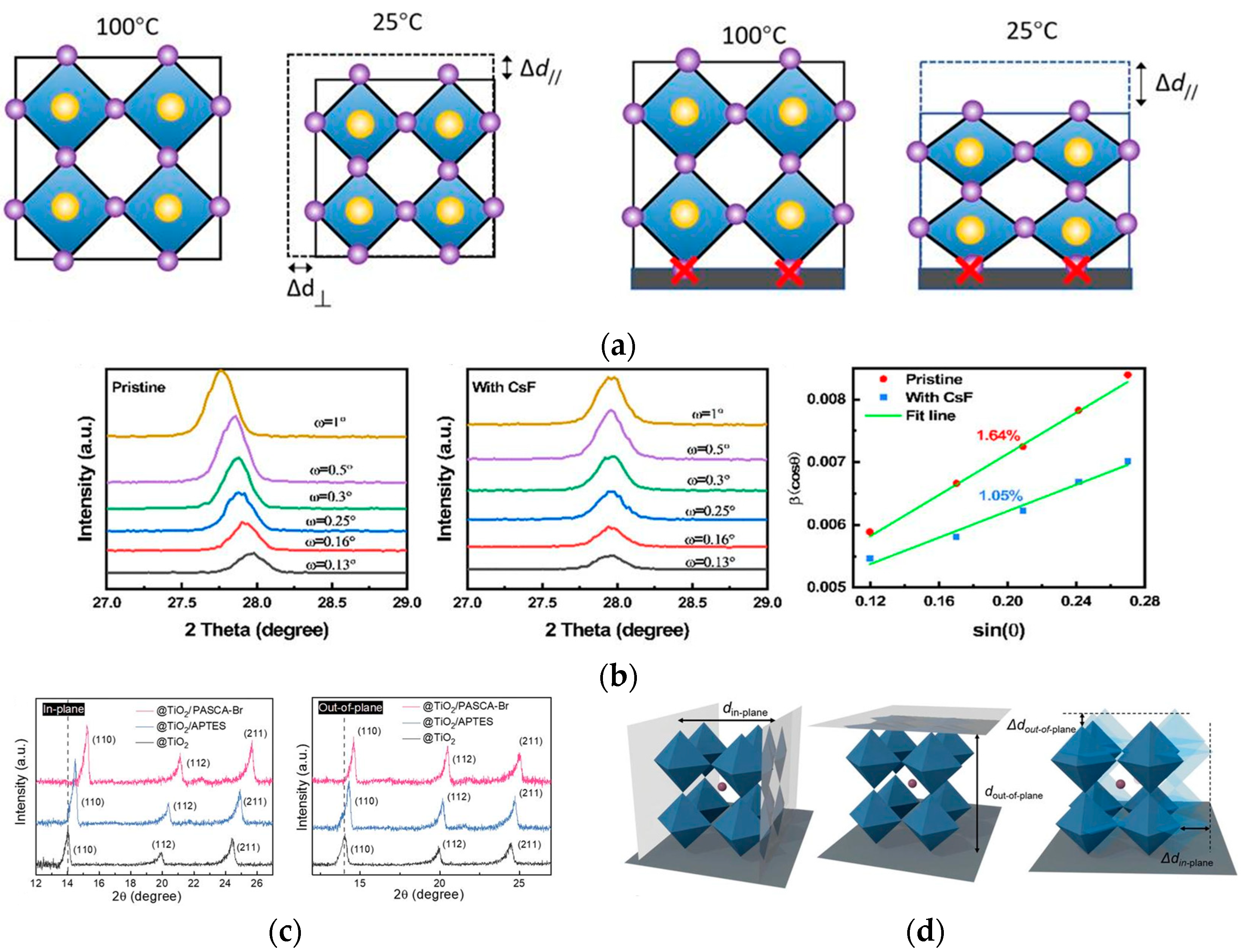
  133. Zhou, Q.; He, D.; Zhuang, Q.; Liu, B.; Li, R.; Li, H.; Zhang, Z.; Yang, H.; Zhao, P.; He, Y.; et al. Revealing Steric-Hindrance-Dependent Buried Interface Defect Passivation Mechanism in Efficient and Stable Perovskite Solar Cells with Mitigated Tensile Stress. Adv. Funct. Mater. 2022, 32, 2205507. [Google Scholar] [CrossRef]
  134. Fu, J.; Zhang, J.; Zhang, T.; Yuan, L.; Zhang, Z.; Jiang, Z.; Huang, Z.; Wu, T.; Yan, K.; Zhang, L.; et al. Synergistic Effects of Interfacial Energy Level Regulation and Stress Relaxation via a Buried Interface for Highly Efficient Perovskite Solar Cells. ACS Nano 2023, 17, 2802–2812. [Google Scholar] [CrossRef] [PubMed]
  135. Yang, M.; Han, G.; Xiao, Y.; Hou, W. Potassium nitrilotriacetate as a multifunctional modifier of the buried interface for hysteresis-reduced perovskite solar cells. Chem. Commun. 2022, 58, 5638–5641. [Google Scholar] [CrossRef] [PubMed]
  136. Wang, L.; Xia, J.; Yan, Z.; Song, P.; Zhen, C.; Jiang, X.; Shao, G.; Qiu, Z.; Wei, Z.; Qiu, J.; et al. Robust Interfacial Modifier for Efficient Perovskite Solar Cells: Reconstruction of Energy Alignment at Buried Interface by Self-Diffusion of Dopants. Adv. Funct. Mater. 2022, 32, 2204725. [Google Scholar] [CrossRef]
  137. Guan, N.; Ran, C.; Wang, Y.; Chao, L.; Deng, Z.; Wu, G.; Dong, H.; Bao, Y.; Lin, Z.; Song, L. SnO2 Passivation and Enhanced Perovskite Charge Extraction with a Benzylamine Hydrochloric Interlayer. ACS Appl. Mater. Interfaces 2022, 14, 34198–34207. [Google Scholar] [CrossRef] [PubMed]
  138. Ma, H.; Wang, M.; Wang, Y.; Dong, Q.; Liu, J.; Yin, Y.; Zhang, J.; Pei, M.; Zhang, L.; Cai, W.; et al. Asymmetric organic diammonium salt buried in SnO2 layer enables fast carrier transfer and interfacial defects passivation for efficient perovskite solar cells. Chem. Eng. J. 2022, 442, 136291. [Google Scholar] [CrossRef]
  139. Zhang, D.; Zhang, X.; Guo, T.; Zou, J.; Zhou, Y.; Jin, J.; Zhu, Z.; Cao, Q.; Zhang, J.; Tai, Q. Small Molecules Functionalized Zinc Oxide Interlayers for High Performance Low-Temperature Carbon-Based CsPbI2 Br Perovskite Solar Cells. Small 2023, 19, e2205604. [Google Scholar] [CrossRef]
  140. Xiong, Z.; Lan, L.; Wang, Y.; Lu, C.; Qin, S.; Chen, S.; Zhou, L.; Zhu, C.; Li, S.; Meng, L.; et al. Multifunctional Polymer Framework Modified SnO2 Enabling a Photostable α-FAPbI3 Perovskite Solar Cell with Efficiency Exceeding 23%. ACS Energy Lett. 2021, 6, 3824–3830. [Google Scholar] [CrossRef]
  141. Wang, J.; Datta, K.; Weijtens, C.H.L.; Wienk, M.M.; Janssen, R.A.J. Insights into Fullerene Passivation of SnO2 Electron Transport Layers in Perovskite Solar Cells. Adv. Funct. Mater. 2019, 29, 1905883. [Google Scholar] [CrossRef] [Green Version]
  142. Gao, Z.W.; Wang, Y.; Liu, H.; Sun, J.; Kim, J.; Li, Y.; Xu, B.; Choy, W.C.H. Tailoring the Interface in FAPbI3 Planar Perovskite Solar Cells by Imidazole-Graphene-Quantum-Dots. Adv. Funct. Mater. 2021, 31, 2101438. [Google Scholar] [CrossRef]
  143. Li, W.; Zhang, W.; Van Reenen, S.; Sutton, R.J.; Fan, J.; Haghighirad, A.A.; Johnston, M.B.; Wang, L.; Snaith, H.J. Enhanced UV-light stability of planar heterojunction perovskite solar cells with caesium bromide interface modification. Energy Environ. Sci. 2016, 9, 490–498. [Google Scholar] [CrossRef] [Green Version]
  144. Wu, M.; Duan, Y.; Yang, L.; You, P.; Li, Z.; Wang, J.; Zhou, H.; Yang, S.; Xu, D.; Zou, H.; et al. Multifunctional Small Molecule as Buried Interface Passivator for Efficient Planar Perovskite Solar Cells. Adv. Funct. Mater. 2023, 33, 2300128. [Google Scholar] [CrossRef]
  145. Jung, E.H.; Chen, B.; Bertens, K.; Vafaie, M.; Teale, S.; Proppe, A.; Hou, Y.; Zhu, T.; Zheng, C.; Sargent, E.H. Bifunctional Surface Engineering on SnO2 Reduces Energy Loss in Perovskite Solar Cells. ACS Energy Lett. 2020, 5, 2796–2801. [Google Scholar] [CrossRef]
  146. Agresti, A.; Pazniak, A.; Pescetelli, S.; Di Vito, A.; Rossi, D.; Pecchia, A.; Auf der Maur, M.; Liedl, A.; Larciprete, R.; Kuznetsov, D.V.; et al. Titanium-carbide MXenes for work function and interface engineering in perovskite solar cells. Nat. Mater. 2019, 18, 1228–1234. [Google Scholar] [CrossRef] [PubMed] [Green Version]
  147. Choi, K.; Lee, J.; Kim, H.I.; Park, C.W.; Kim, G.-W.; Choi, H.; Park, S.; Park, S.A.; Park, T. Thermally stable, planar hybrid perovskite solar cells with high efficiency. Energy Environ. Sci. 2018, 11, 3238–3247. [Google Scholar] [CrossRef]
  148. Liu, C.; Huang, L.; Zhou, X.; Wang, X.; Yao, J.; Liu, Z.; Liu, S.F.; Ma, W.; Xu, B. An in-situ defect passivation through a green anti-solvent approach for high-efficiency and stable perovskite solar cells. Sci. Bull. 2021, 66, 1419–1428. [Google Scholar] [CrossRef]
  149. Altinkaya, C.; Aydin, E.; Ugur, E.; Isikgor, F.H.; Subbiah, A.S.; De Bastiani, M.; Liu, J.; Babayigit, A.; Allen, T.G.; Laquai, F.; et al. Tin Oxide Electron-Selective Layers for Efficient, Stable, and Scalable Perovskite Solar Cells. Adv. Mater. 2021, 33, e2005504. [Google Scholar] [CrossRef]
  150. Yu, W.; Sun, X.; Xiao, M.; Hou, T.; Liu, X.; Zheng, B.; Yu, H.; Zhang, M.; Huang, Y.; Hao, X. Recent advances on interface engineering of perovskite solar cells. Nano Res. 2021, 15, 85–103. [Google Scholar] [CrossRef]
  151. Hassan, A.; Wang, Z.; Ahn, Y.H.; Azam, M.; Khan, A.A.; Farooq, U.; Zubair, M.; Cao, Y. Recent defect passivation drifts and role of additive engineering in perovskite photovoltaics. Nano Energy 2022, 101, 107579. [Google Scholar] [CrossRef]
  152. Guo, H.; Yang, C.Y.; Zhang, X.; Motta, A.; Feng, K.; Xia, Y.; Shi, Y.; Wu, Z.; Yang, K.; Chen, J.; et al. Transition metal-catalysed molecular n-doping of organic semiconductors. Nature 2021, 599, 67–73. [Google Scholar] [CrossRef]
  153. Tan, H.; Jain, A.; Voznyy, O.; Lan, X.; de Arquer, F.P.G.; Fan, J.Z.; Quintero-Bermudez, R.; Yuan, M.; Zhang, B.; Zhao, Y.; et al. Efficient and stable solution-processed planar perovskite solar cells via contact passivation. Science 2017, 355, 722–726. [Google Scholar] [CrossRef]
  154. Li, Z.; Wang, L.; Liu, R.; Fan, Y.; Meng, H.; Shao, Z.; Cui, G.; Pang, S. Spontaneous Interface Ion Exchange: Passivating Surface Defects of Perovskite Solar Cells with Enhanced Photovoltage. Adv. Energy Mater. 2019, 9, 1902142. [Google Scholar] [CrossRef]
  155. Bu, T.; Li, J.; Zheng, F.; Chen, W.; Wen, X.; Ku, Z.; Peng, Y.; Zhong, J.; Cheng, Y.B.; Huang, F. Universal passivation strategy to slot-die printed SnO2 for hysteresis-free efficient flexible perovskite solar module. Nat. Commun. 2018, 9, 4609. [Google Scholar] [CrossRef] [PubMed] [Green Version]
  156. Liu, X.; Zhang, Y.; Shi, L.; Liu, Z.; Huang, J.; Yun, J.S.; Zeng, Y.; Pu, A.; Sun, K.; Hameiri, Z.; et al. Exploring Inorganic Binary Alkaline Halide to Passivate Defects in Low-Temperature-Processed Planar-Structure Hybrid Perovskite Solar Cells. Adv. Energy Mater. 2018, 8, 1800138. [Google Scholar] [CrossRef]
  157. Zhu, P.; Gu, S.; Luo, X.; Gao, Y.; Li, S.; Zhu, J.; Tan, H. Simultaneous Contact and Grain-Boundary Passivation in Planar Perovskite Solar Cells Using SnO2-KCl Composite Electron Transport Layer. Adv. Energy Mater. 2019, 10, 1903083. [Google Scholar] [CrossRef]
  158. Xu, H.; Miao, Y.; Wei, N.; Chen, H.; Qin, Z.; Liu, X.; Wang, X.; Qi, Y.; Zhang, T.; Zhao, Y. CsI Enhanced Buried Interface for Efficient and UV-Robust Perovskite Solar Cells. Adv. Energy Mater. 2021, 12, 2103151. [Google Scholar] [CrossRef]
  159. Wang, J.; Wang, Z.; Chen, S.; Jiang, N.; Yuan, L.; Zhang, J.; Duan, Y. Reduced Surface Hydroxyl and Released Interfacial Strain by Inserting CsF Anchor Interlayer for High-Performance Perovskite Solar Cells. Sol. RRL 2022, 7, 2200960. [Google Scholar] [CrossRef]
  160. Boehm, H.P. Acidic and basic properties of hydroxylated metal-oxide surfaces. Discuss. Faraday Soc. 1971, 52, 264–275. [Google Scholar] [CrossRef]
  161. Gong, C.; Zhang, C.; Zhuang, Q.; Li, H.; Yang, H.; Chen, J.; Zang, Z. Stabilizing Buried Interface via Synergistic Effect of Fluorine and Sulfonyl Functional Groups Toward Efficient and Stable Perovskite Solar Cells. Nanomicro Lett. 2022, 15, 17. [Google Scholar] [CrossRef]
  162. Bi, H.; Liu, B.; He, D.; Bai, L.; Wang, W.; Zang, Z.; Chen, J. Interfacial defect passivation and stress release by multifunctional KPF6 modification for planar perovskite solar cells with enhanced efficiency and stability. Chem. Eng. J. 2021, 418, 129375. [Google Scholar] [CrossRef]
  163. Xu, C.; Zhang, S.; Fan, W.; Cheng, F.; Sun, H.; Kang, Z.; Zhang, Y. Pushing the Limit of Open-Circuit Voltage Deficit via Modifying Buried Interface in CsPbI2 Perovskite Solar Cells. Adv. Mater. 2023, 35, e2207172. [Google Scholar] [CrossRef]
  164. Liu, T.; Guo, X.; Liu, Y.; Hou, M.; Yuan, Y.; Mai, X.; Fedorovich, K.V.; Wang, N. 4-Trifluorophenylammonium Iodide-Based Dual Interfacial Modification Engineering toward Improved Efficiency and Stability of SnO2-Based Perovskite Solar Cells. ACS Appl. Mater. Interfaces 2023, 15, 6777–6787. [Google Scholar] [CrossRef] [PubMed]
  165. Yang, M.; Hu, R.; Kang, J.; Xiao, Y.; Han, G.; Hou, W. Amidine thiourea as a multifunctional modifier of buried interface for effective perovskite solar cells with reduced lead leakage. Org. Electron. 2022, 111, 106656. [Google Scholar] [CrossRef]
  166. Chen, J.; Zhao, X.; Kim, S.G.; Park, N.G. Multifunctional Chemical Linker Imidazoleacetic Acid Hydrochloride for 21% Efficient and Stable Planar Perovskite Solar Cells. Adv. Mater. 2019, 31, e1902902. [Google Scholar] [CrossRef] [PubMed]
  167. Zuo, X.; Kim, B.; Liu, B.; He, D.; Bai, L.; Wang, W.; Xu, C.; Song, Q.; Jia, C.; Zang, Z.; et al. Passivating buried interface via self-assembled novel sulfonium salt toward stable and efficient perovskite solar cells. Chem. Eng. J. 2022, 431, 133209. [Google Scholar] [CrossRef]
  168. Ren, X.; Liu, Y.; Lee, D.G.; Kim, W.B.; Han, G.S.; Jung, H.S.; Liu, S. Chlorine-modified SnO2 electron transport layer for high-efficiency perovskite solar cells. InfoMat 2019, 2, 401–408. [Google Scholar] [CrossRef] [Green Version]
  169. Min, H.; Lee, D.Y.; Kim, J.; Kim, G.; Lee, K.S.; Kim, J.; Paik, M.J.; Kim, Y.K.; Kim, K.S.; Kim, M.G.; et al. Perovskite solar cells with atomically coherent interlayers on SnO2 electrodes. Nature 2021, 598, 444–450. [Google Scholar] [CrossRef]
  170. Yi, Z.; Xiao, B.; Li, X.; Luo, Y.; Jiang, Q.; Yang, J. Novel dual-modification strategy using Ce-containing compounds toward high-performance flexible perovskite solar cells. Nano Energy 2023, 109, 108241. [Google Scholar] [CrossRef]
  171. Tian, J.; Xue, Q.; Tang, X.; Chen, Y.; Li, N.; Hu, Z.; Shi, T.; Wang, X.; Huang, F.; Brabec, C.J.; et al. Dual Interfacial Design for Efficient CsPbI3 Br Perovskite Solar Cells with Improved Photostability. Adv. Mater. 2019, 31, e1901152. [Google Scholar] [CrossRef]
  172. Zhang, Y.; Kong, T.; Xie, H.; Song, J.; Li, Y.; Ai, Y.; Han, Y.; Bi, D. Molecularly Tailored SnO2/Perovskite Interface Enabling Efficient and Stable FAPbI3 Solar Cells. ACS Energy Lett. 2022, 7, 929–938. [Google Scholar] [CrossRef]
  173. Yang, W.S.; Noh, J.H.; Jeon, N.J.; Kim, Y.C.; Ryu, S.; Seo, J.; Seok, S.I. High-performance photovoltaic perovskite layers fabricated through intramolecular exchange. Science 2015, 348, 1234–1237. [Google Scholar] [CrossRef]
  174. Bi, D.; Yi, C.; Luo, J.; Décoppet, J.-D.; Zhang, F.; Zakeeruddin, S.M.; Li, X.; Hagfeldt, A.; Grätzel, M. Polymer-templated nucleation and crystal growth of perovskite films for solar cells with efficiency greater than 21%. Nat. Energy 2016, 1, 16142. [Google Scholar] [CrossRef]
  175. Hui, W.; Chao, L.; Lu, H.; Xia, F.; Wei, Q.; Su, Z.; Niu, T.; Tao, L.; Du, B.; Li, D.; et al. Stabilizing black-phase formamidinium perovskite formation at room temperature and high humidity. Science 2021, 371, 1359. [Google Scholar] [CrossRef] [PubMed]
  176. Liang, Y.; Shang, Q.; Li, M.; Zhang, S.; Liu, X.; Zhang, Q. Solvent Recrystallization-Enabled Green Amplified Spontaneous Emissions with an Ultra-Low Threshold from Pinhole-Free Perovskite Films. Adv. Funct. Mater. 2021, 31, 2106108. [Google Scholar] [CrossRef]
  177. Zhang, F.; Xiao, C.; Chen, X.; Larson, B.W.; Harvey, S.P.; Berry, J.J.; Zhu, K. Self-Seeding Growth for Perovskite Solar Cells with Enhanced Stability. Joule 2019, 3, 1452–1463. [Google Scholar] [CrossRef]
  178. Jung, M.; Ji, S.G.; Kim, G.; Seok, S.I. Perovskite precursor solution chemistry: From fundamentals to photovoltaic applications. Chem. Soc. Rev. 2019, 48, 2011–2038. [Google Scholar] [CrossRef]
  179. Lohmann, K.B.; Patel, J.B.; Rothmann, M.U.; Xia, C.Q.; Oliver, R.D.J.; Herz, L.M.; Snaith, H.J.; Johnston, M.B. Control over Crystal Size in Vapor Deposited Metal-Halide Perovskite Films. ACS Energy Lett. 2020, 5, 710–717. [Google Scholar] [CrossRef]
  180. Luo, D.; Yang, W.; Wang, Z.; Sadhanala, A.; Hu, Q.; Su, R.; Shivanna, R.; Trindade, G.F.; Watts, J.F.; Xu, Z.; et al. Enhanced photovoltage for inverted planar heterojunction perovskite solar cells. Science 2018, 360, 1442–1446. [Google Scholar] [CrossRef] [Green Version]
  181. Liu, Z.; Qiu, L.; Ono, L.K.; He, S.; Hu, Z.; Jiang, M.; Tong, G.; Wu, Z.; Jiang, Y.; Son, D.-Y.; et al. A holistic approach to interface stabilization for efficient perovskite solar modules with over 2,000-hour operational stability. Nat. Energy 2020, 5, 596–604. [Google Scholar] [CrossRef]
  182. Chen, K.; Wu, P.; Yang, W.; Su, R.; Luo, D.; Yang, X.; Tu, Y.; Zhu, R.; Gong, Q. Low-dimensional perovskite interlayer for highly efficient lead-free formamidinium tin iodide perovskite solar cells. Nano Energy 2018, 49, 411–418. [Google Scholar] [CrossRef]
  183. Steele, J.A.; Jin, H.; Dovgaliuk, I.; Berger, R.F.; Braeckevelt, T.; Yuan, H.; Martin, C.; Solano, E.; Lejaeghere, K.; Rogge, S.M.J.; et al. Thermal unequilibrium of strained black CsPbI3 thin films. Science 2019, 365, 679–684. [Google Scholar] [CrossRef]
  184. Zhu, C.; Niu, X.; Fu, Y.; Li, N.; Hu, C.; Chen, Y.; He, X.; Na, G.; Liu, P.; Zai, H.; et al. Strain engineering in perovskite solar cells and its impacts on carrier dynamics. Nat. Commun. 2019, 10, 815. [Google Scholar] [CrossRef] [PubMed] [Green Version]
  185. Misra, R.K.; Aharon, S.; Li, B.; Mogilyansky, D.; Visoly-Fisher, I.; Etgar, L.; Katz, E.A. Temperature- and Component-Dependent Degradation of Perovskite Photovoltaic Materials under Concentrated Sunlight. J. Phys. Chem. Lett. 2015, 6, 326–330. [Google Scholar] [CrossRef]
  186. Chen, Q.; Zhou, H.; Song, T.B.; Luo, S.; Hong, Z.; Duan, H.S.; Dou, L.; Liu, Y.; Yang, Y. Controllable self-induced passivation of hybrid lead iodide perovskites toward high performance solar cells. Nano Lett. 2014, 14, 4158–4163. [Google Scholar] [CrossRef] [PubMed]
  187. Calloni, A.; Abate, A.; Bussetti, G.; Berti, G.; Yivlialin, R.; Ciccacci, F.; Duò, L. Stability of Organic Cations in Solution-Processed CH3NH3PbI3 Perovskites: Formation of Modified Surface Layers. J. Phys. Chem. C 2015, 119, 21329–21335. [Google Scholar] [CrossRef]
  188. Kim, Y.C.; Jeon, N.J.; Noh, J.H.; Yang, W.S.; Seo, J.; Yun, J.S.; Ho-Baillie, A.; Huang, S.; Green, M.A.; Seidel, J.; et al. Beneficial Effects of PbI2 Incorporated in Organo-Lead Halide Perovskite Solar Cells. Adv. Energy Mater. 2016, 6, 1502104. [Google Scholar] [CrossRef]
  189. Qin, Z.; Chen, Y.; Wang, X.; Wei, N.; Liu, X.; Chen, H.; Miao, Y.; Zhao, Y. Zwitterion-Functionalized SnO2 Substrate Induced Sequential Deposition of Black-Phase FAPbI3 with Rearranged PbI2 Residue. Adv. Mater. 2022, 34, e2203143. [Google Scholar] [CrossRef]
  190. Luo, C.; Zhao, Y.; Wang, X.; Gao, F.; Zhao, Q. Self-Induced Type-I Band Alignment at Surface Grain Boundaries for Highly Efficient and Stable Perovskite Solar Cells. Adv. Mater. 2021, 33, e2103231. [Google Scholar] [CrossRef]
  191. Deng, C.; Wu, J.; Yang, Y.; Du, Y.; Li, R.; Chen, Q.; Xu, Y.; Sun, W.; Lan, Z.; Gao, P. Modulating Residual Lead Iodide via Functionalized Buried Interface for Efficient and Stable Perovskite Solar Cells. ACS Energy Lett. 2022, 8, 666–676. [Google Scholar] [CrossRef]
  192. Sun, W.; Wang, K.; Liu, W.; Huo, X.; Yin, R.; Sun, Y.; Gao, Y.; You, T.; Yin, P. Bidirectional Modification of Buried Interface Reduces Energy Loss for Planar Perovskite Solar Cells with Efficiency >23%. Sol. RRL 2023, 7, 2200991. [Google Scholar] [CrossRef]
  193. Zhuang, Q.; Zhang, C.; Gong, C.; Li, H.; Li, H.; Zhang, Z.; Yang, H.; Chen, J.; Zang, Z. Tailoring multifunctional anion modifiers to modulate interfacial chemical interactions for efficient and stable perovskite solar cells. Nano Energy 2022, 102, 107747. [Google Scholar] [CrossRef]
  194. Chen, Y.; Wang, Q.; Tang, W.; Qiu, W.; Wu, Y.; Peng, Q. Heterocyclic amino acid molecule as a multifunctional interfacial bridge for improving the efficiency and stability of quadruple cation perovskite solar cells. Nano Energy 2023, 107, 108154. [Google Scholar] [CrossRef]
  195. Ren, J.; Liu, T.; He, B.; Wu, G.; Gu, H.; Wang, B.; Li, J.; Mao, Y.; Chen, S.; Xing, G. Passivating Defects at the Bottom Interface of Perovskite by Ethylammonium to Improve the Performance of Perovskite Solar Cells. Small 2022, 18, e2203536. [Google Scholar] [CrossRef]
  196. Zhao, J.; Deng, Y.; Wei, H.; Zheng, X.; Yu, Z.; Shao, Y.; Shield, J.E.; Huang, J. Strained hybrid perovskite thin films and their impact on the intrinsic stability of perovskite solar cells. Sci. Adv. 2017, 3, eaao5616. [Google Scholar] [CrossRef] [PubMed] [Green Version]
  197. Jones, T.W.; Osherov, A.; Alsari, M.; Sponseller, M.; Duck, B.C.; Jung, Y.-K.; Settens, C.; Niroui, F.; Brenes, R.; Stan, C.V.; et al. Lattice strain causes non-radiative losses in halide perovskites. Energy Environ. Sci. 2019, 12, 596–606. [Google Scholar] [CrossRef] [Green Version]
  198. Doherty, T.A.S.; Winchester, A.J.; Macpherson, S.; Johnstone, D.N.; Pareek, V.; Tennyson, E.M.; Kosar, S.; Kosasih, F.U.; Anaya, M.; Abdi-Jalebi, M.; et al. Performance-limiting nanoscale trap clusters at grain junctions in halide perovskites. Nature 2020, 580, 360–366. [Google Scholar] [CrossRef]
  199. Zhang, C.C.; Yuan, S.; Lou, Y.H.; Liu, Q.W.; Li, M.; Okada, H.; Wang, Z.K. Perovskite Films with Reduced Interfacial Strains via a Molecular-Level Flexible Interlayer for Photovoltaic Application. Adv. Mater. 2020, 32, e2001479. [Google Scholar] [CrossRef]
  200. Bai, Y.; Chen, H.; Xiao, S.; Xue, Q.; Zhang, T.; Zhu, Z.; Li, Q.; Hu, C.; Yang, Y.; Hu, Z.; et al. Effects of a Molecular Monolayer Modification of NiO Nanocrystal Layer Surfaces on Perovskite Crystallization and Interface Contact toward Faster Hole Extraction and Higher Photovoltaic Performance. Adv. Funct. Mater. 2016, 26, 2950–2958. [Google Scholar] [CrossRef]
  201. Chen, W.; Zhou, Y.; Wang, L.; Wu, Y.; Tu, B.; Yu, B.; Liu, F.; Tam, H.W.; Wang, G.; Djurisic, A.B.; et al. Molecule-Doped Nickel Oxide: Verified Charge Transfer and Planar Inverted Mixed Cation Perovskite Solar Cell. Adv. Mater. 2018, 30, e1800515. [Google Scholar] [CrossRef]
  202. Ahmad, S.; Ma, R.; Zheng, J.; Gary Kwok, C.K.; Zhou, Q.; Ren, Z.; Kim, J.; He, X.; Zhang, X.; Yu, K.M.; et al. Suppressing Nickel Oxide/Perovskite Interface Redox Reaction and Defects for Highly Performed and Stable Inverted Perovskite Solar Cells. Small Methods 2022, 6, e2200787. [Google Scholar] [CrossRef]
  203. Wei, J.; Guo, F.; Wang, X.; Xu, K.; Lei, M.; Liang, Y.; Zhao, Y.; Xu, D. SnO2 -in-Polymer Matrix for High-Efficiency Perovskite Solar Cells with Improved Reproducibility and Stability. Adv. Mater. 2018, 30, e1805153. [Google Scholar] [CrossRef]
  204. Hui, W.; Yang, Y.; Xu, Q.; Gu, H.; Feng, S.; Su, Z.; Zhang, M.; Wang, J.; Li, X.; Fang, J.; et al. Red-Carbon-Quantum-Dot-Doped SnO2 Composite with Enhanced Electron Mobility for Efficient and Stable Perovskite Solar Cells. Adv. Mater. 2020, 32, e1906374. [Google Scholar] [CrossRef] [PubMed]
Figure 1. Main progress of the conversion efficiency of perovskite solar cells in the last decade [7].
Energies 16 05015 g001
Figure 4. (a) Stripping exposes the buried interface. (b) SEM images of upper and lower surfaces of perovskite films. (c) Nano-FTIR images of upper and lower surfaces of perovskite films [18].
Energies 16 05015 g004
Figure 7. Schematic representation of interfaces in PSCs with a planar structure [28].
Energies 16 05015 g007
Figure 8. Diagrams illustrating the band alignment at the ETL/Perovskite interface with (a) type I: straddling gap and (b) type II: staggered gap [97].
Energies 16 05015 g008
Figure 11. (a) Trap-like localized antisite defects form near the valence band edge of the PbI2-terminated TiO2/perovskite interface that is shallow and delocalized [153]. (b) Schematic diagram of the perovskite growth process [155]. (c) Steady-state and time-resolved PL (TRPL) spectra of perovskite films on SnO2 and SnO2-KCl [157]. (d) O1s and F1s XPS spectra of SnO2 and CsF-SnO2 films [159]. (e) Schematic illustration of NH4F treatment on SnO2 surface [145].
Energies 16 05015 g011
Figure 12. (a) The morphology and distribution of lead iodide before and after modification with a passivating agent [191]. (b) Overhead scanning electron microscope (SEM) image of PbI2 film and perovskite film deposited on SnO2 and SnO2/NiAc2 and the SEM image of the cross section of the film [192]. (c) Top-view SEM images of the PbI2 and perovskite films deposited on SnO2 substrates with and without GA salt modification [193]. (d) AFM images of SnO2 and FSA-SnO2 films [194]. (e) Top-view SEM images of control and FSA-FAPbI3 perovskite films [194].
Energies 16 05015 g012
Figure 13. Schematic diagram: (a) Without a substrate, the perovskite forming at 100 °C contracts vertically and laterally during cooling, and with the substrate adhesion, the annealed perovskite film only contracts vertically [196]. (b) XRD patterns and lattice strain patterns of perovskite films prepared on SnO2 and CsF-SnO2 substrates [159]. (c) In-plane and out-of-plane GIXRD results for perovskite films deposited on TiO2, TiO2/APTES, and TiO2/PASCA-Br substrates, respectively, and (d) the corresponding crystal strains of perovskite films at in-plane and out-of-plane directions [199].
Energies 16 05015 g013
Table 1. A review on the application of different kinds of materials to the PSCs buried layer interface modification. Device architecture and key parameters are provided.
Device StructureJsc (mA/cm2)Voc (V)FF (%)PCE (%)Ref.
ITO/SnO2/IT-4F/(FAPbI3)x(MAPbBr3)1−x/Spiro-MeOTAD/MoO3/Ag24.871.1781.5623.73[134]
ITO/SnO2/NTAK/(Cs0.05FA0.54MA0.41)Pb(I0.98Br0.02)3/Spiro-OMeTAD/Ag24.951.087821.02[135]
ITO/SnO2/PL-A/perovskite/Spiro-OMeTAD/Au24.491.1981.4723.74[136]
ITO/SnO2/BH/MAPbI3/Spiro-OMeTAD/MoO3/Ag22.831.1578.8720.74[137]
FTO/SnO2/DMAPAI2/perovskite/Spiro-OMeTAD/Ag24.201.1782.1923.20[138]
ITO/SnO2/ZnO (doped ZnO)/CsPbI2Br/carbon14.951.25574.313.94[139]
ITO/SnO2/PEGDA/FAPbI3/Spiro-OMeTAD/MoO3/Ag25.241.1481.0023.31[140]
ITO/SnO2/PCBA/FA0.66MA0.34PbI2.85Br0.15/Spiro-OMeTAD/MoO3/Au22.21.1076.0018.6[141]
ITO/SnO2/PCBM/FA0.66MA0.34PbI2.85Br0.15/Spiro-OMeTAD/MoO3/Au22.11.0872.0017.1
ITO/SnO2/C60/FA0.66MA0.34PbI2.85Br0.15/Spiro-OMeTAD/MoO3/Au21.41.0469.0015.3
ITO/SnO2/I-GQDs/FAPbI3/Spiro-OMeTAD/Ag25.421.07382.0022.37[142]
FTO/cTiO2/CsBr/MAPbI3−xClx/Spiro-OMeTAD/Au20.71.067516.3[143]
FTO/SnO2/PBGH/FA0.9Cs0.1PbI3/Spiro-OMeTAD/Au25.021.19782.7624.79[144]
FTO/SnO2/NH4F/(FAPbI3)0.95(MAPbBr3)0.05/Spiro-OMeTAD/Au24.61.1681.123.2[145]
FTO/cTiO2/MXeneTi3C2Tx/MAPbI3/spiro-OMeTAD/Au23.821.0977.620.14[146]
FTO/SnO2/zwitterionic compound/Cs0.05(FA0.83MA0.17)0.95
PbI2.55Br0.45/Spiro-MeOTAD/Au
23.61.1678.421.43[147]
ITO/ZnO/3-APA (SAM)/MAPbI3/Spiro-MeOTAD/MoO3/Ag22.511.076515.67[131]
FTO/TiO2/Dopamine(DA)/Cs0.05FA0.81MA0.14PbI2.55Br0.45/Spiro-MeOTAD/Au23.651.167620.93[120]
Disclaimer/Publisher’s Note: The statements, opinions and data contained in all publications are solely those of the individual author(s) and contributor(s) and not of MDPI and/or the editor(s). MDPI and/or the editor(s) disclaim responsibility for any injury to people or property resulting from any ideas, methods, instructions or products referred to in the content.

