Article

Performance of Cs-Doped Carbon-Based Perovskite Solar Cells in Ambient Environment

1
U.S.-Pakistan Centre for Advanced Studies in Energy (USPCAS-E), National University of Sciences and Technology (NUST), H-12, Islamabad 44000, Pakistan
2
School of Chemical and Materials Engineering (SCME), National University of Sciences and Technology (NUST), H-12, Islamabad 44000, Pakistan
3
Nanosciences and Technology Department (NS&TD), National Centre for Physics (NCP), Islamabad 44000, Pakistan
4
Department of Applied Science and Technology (DISAT) and RU INSTM, Politecnico di Torino, 10129 Torino, Italy
*
Author to whom correspondence should be addressed.
Energies 2023, 16(12), 4748; https://doi.org/10.3390/en16124748
Submission received: 23 May 2023 / Revised: 12 June 2023 / Accepted: 14 June 2023 / Published: 15 June 2023
(This article belongs to the Special Issue Recent Advances in Solar Cells and Photovoltaics)

Abstract

:
The development of organometal halide-based perovskite solar cells (PSCs) has made remarkable progress in photovoltaics. The commercialization of PSCs is still significantly limited, owing to their poor stability and the high material cost of a hole transport layer (HTL) and metal electrodes. To counter these issues, a carbon-based HTL and noble metal-free PSCs are being used. In this work, the effect of Cs-doping on perovskite film morphology and device performance has been systematically studied because the Cs+ and Br ions-doping has proved to be a good choice to improve the stability of PSCs in combination with a carbon electrode. The results showed that when the Cs-doping concentration in perovskite film, MA1−xCsxPb(I1−yBry)3, was equal to x = 0.09, there was a substantial change in the morphological and optoelectronic properties of perovskite films. The grain size of perovskite films was improved from 70 nm (x = 0.00 control) to 170 nm (x = 0.09 Cs-doped), reducing grain boundaries. Moreover, the trap states were additionally passivated resulting in improved radiative recombinations in the perovskite film. The device fabrication was carried out in a controlled dry glovebox, with relative humidity < 40% using carbon as a counter electrode. As a result, Cs-doped PSCs showed a significant increase in efficiency (5.27%) compared to control PSCs (1.55%).

Graphical Abstract

1. Introduction

The advancements in optoelectronic materials have not only changed human life in the present, however have indicated a bright future ahead. The research has shifted toward organic–inorganic perovskites, due to their surprising optoelectronic properties having great potential to revolutionize photovoltaic (PV) applications [1]. Many promising properties of PSCs have rendered them the most appropriate choice for application in PV technologies [2,3,4]. These properties include a low cost of fabrication [5], high absorption coefficient, high power conversion efficiency (PCE), and long electron–hole diffusion length [6,7]. By varying the chemical composition of hybrid lead halide perovskite materials, their morphological, as well as optoelectronic properties, can be tuned. The PCE of hybrid organic–inorganic PSCs has increased from 3.8 up to 25.8% in a matter of a few years [8,9,10]. The major hindrance in their commercial application is their operating life, mainly due to decomposition under the influence of ultraviolet (UV) light, moisture, and oxygen. The stability issue is currently being addressed using various techniques, which include the employment of charge transport layers of hydrophobic materials, the optimization of fabrication techniques, the device encapsulation with hydrophobic and inert materials for better sealing, the modification of the electron transport layer (ETL) interface, and the tuning of perovskite materials with mixed halides or more stable organic cations, etc. [11]. Further, ABX3 represents the structure of PSCs’ light-absorbing layer, where A denotes methyl ammonium (CH3NH3 (MA)) or formamidinium (NH2CHNH2 (FA)) cations, B denotes bivalent metal (Pb or Sn), and X denotes halide or mixed halides (Cl, Br or I) [12]. The PV performance of mixed halide PSCs can be enhanced by tuning the I/Br ratio, and using this approach, a PCE of 12.3% was reported for MAPb(I1−xBrx)3 PSCs [13,14].
Nevertheless, the use of organic cations compromises the long-term stability of PSCs. Inorganic cations, as a replacement for organic cations, have been reported to be a more suitable choice for enhancing the device’s stability, whereas hybrid cations, on the other hand, undergo an accelerated decomposition at higher temperature values. The appropriate tolerance factor of Cs makes CsPbI3 a promising inorganic perovskite material [15]. However, upon heating to 320 °C, cubic black or an α-phase is observed whereas at room temperature the CsPbI3 film presents a δ-phase or, in other words, an orthorhombic yellow phase [16]. Using bication component incorporation, solvent engineering, and halogen exchange techniques, the α-CsPbI3 phase stability could be improved. Moreover, applying structures with lower dimensions has been proved to enhance PSCs’ stability. Materials such as CH3NH3PbI3 have shown an improved stability upon the inclusion of cations with small radii such as Cs, as compared to MA counterparts, thus making it a compatible replacement of MA in the unit cell [17,18]. Saliba et al. [19] introduced CsI into a solution consisting of N,N-dimethylformamide (DMF) and dimethyl sulfoxide (DMSO), which already contained FAI, PbI2, MABr, and PbBr2. The inclusion of inorganic Cs+ led to triple cation perovskite compositions that exhibited an enhanced thermal stability, reduced non-photoactive yellow phase impurities, and decreased sensitivity to processing conditions. In a separate study, Noh et al. [13] constructed inorganic–organic heterojunction solar cells utilizing the entire range of MAPb(I1−xBrx)3 (0 ≤ x ≤ 1). These investigations collectively demonstrate the effective performance enhancement of PSCs through the incorporation of Cs+ and Br- ions via single ion doping.
On the other side, when PSCs are left out to operate for a longer time, the metallic electrodes tend to corrode reducing the device’s lifetime due to oxygen vacancies, iodine, and metal halide ion formation [20,21]. In carbon-based PSCs (C-PSCs), carbon is used as an electrode, and its work function of approximately 5 eV makes it an efficient charge collector. Meanwhile, its hydrophobic nature and inertness help in achieving better stability even without encapsulation as it is neither affected by oxygen nor by ion migration [22,23].
Two types of C-PSCs are commonly reported, i.e., high-temperature (HT) and low-temperature (LT) processed C-PSCs [24]. Both of these structures exhibit the same working principle; however, LT C-PSCs are much simpler in structure as compared to the HT C-PSCs as carbon electrodes are directly deposited on the perovskite structure, which shows the proper crystallization at a low temperature [23]. The maximum efficiency achieved with HT C-PSCs is 16.37%, with a pristine MAPbI3 structure without HTL [25,26]. On the other hand, LT C-PSCs are able to achieve PCEs comparable to those exhibited by Au- and Ag-based devices [23,27]. The simultaneous use of graphite and carbon black has been reported as a high-performing combination, providing better conductivity and mechanical stability along with low series resistance. However, the compatibility between the combinations of carbon paste and additives and the perovskite layer in C-PSCs must be ensured to elude decomposition [28,29].
As discussed earlier, mixed cation/halide PSCs are more stable in the environment as compared to those based on the pristine MAPbI3. The concept of the substitution of HTL with graphite and a metal electrode with carbon black was first practiced by Lyu et al. [30], who reported a device PCE of 6.6%. This breakthrough opened the doors for the fabrication of HTL-, as well as metallic electrode-free PSCs. In another work, Kartikay et. al. fabricated C-PSCs based on fluorine-doped tin oxide (FTO)/TiO2 compact layer/TiO2 mesoporous layer/mixed cation FA1−xMAxPb(IyBr1−y)3 perovskite absorber layer/carbon architecture. By using this structure, they achieved a PCE > 10%, and the unencapsulated device showed a very improved stability over more than 700 h [31]. HTL-free C-PSCs with a device structure consisting of glass/In-doped SnO2/quantum dot (QD)-SnO2/mixed cation Cs0.05FA0.81MA0.14PbI2.55Br0.45 perovskite absorber layer/carbon were developed by Vijayaraghavan et al. and exhibited a PCE of 13.64% [32].
According to our knowledge, there is no literature available on the doping of the perovskite absorber layer with CsBr in a dry environment in combination with carbon as a counter electrode (CE). Most of the literature available is on the triple cation (Cs, MA, FA), synthesized in an inert glove box. In this work, a much simpler method was used to fabricate Cs and Br co-doped perovskite films from a solution of methylammonium iodide (MAI), PbI2, and CsBr in a mixed solvent containing N,N-dimethylformamide (DMF) and dimethyl sulfoxide (DMSO) by spin-coating in a dry glove box at a humidity level of less than 40%. Molar ratios of CsBr:MAI:PbI2 equal to 0:1:1, 0.09:0.91:1, and 0.15:0.85:1 were used to prepare the best quality layer. A LT PSC structure was used for the fabrication of the full device, and a good quality layer with improved efficiency and stability was obtained as compared to the standard layer.

2. Materials and Methods

2.1. Materials

Lead iodide (PbI2, 99.9%), methylammonium iodide (MAI, 99.9%), cesium bromide (CsBr, 99.9%), polyvinyl acetate (PVAc), carbon black and graphite flakes, FTO glass, N,N-dimethylformamide (DMF, anhydrous 99.8%), dimethyl sulfoxide (DMSO, 99.8%), chlorobenzene (CB, anhydrous 99.8%), titanium (IV) isopropoxide (TTIP, 99.9%), and mesoporous titania dioxide (meso-TiO2) were all purchased from Sigma-Aldrich (St. Louis, MO, USA). All reagents were employed as received, without further purification.

2.2. Characterization

The X-ray diffraction (XRD) technique was used (Bruker D8 Advanced, Bruker AXS GmbH, Karlsruhe, Germany) to investigate the structural changes and analyze the crystal size of the perovskite films, employing a scanning rate of 0.02 °/s in the 2θ range of 5 to 70°. The XRD patterns were recorded using a CuKα radiation source (λ = 154056 Å), generated at an excitation voltage of 25 kV and a current of 40 mA.
The ultraviolet–visible–near infrared (UV–Vis–NIR) spectrophotometer UV-3600 Plus (Shimadzu Co., Kyoto, Japan) was used to investigate the optical properties of the perovskite absorber layers. The absorbance of the samples was measured in the range of 350 to 1100 nm.
Photoluminescence (PL) emission spectra in the range of 389 to 1100 nm (380 nm excitation wavelength) were acquired, using the iHR-320 spectrophotometer of Horiba Scientific (Horiba Instruments Inc., Irvine, CA, USA).
The Fourier transform infrared spectroscopy (FTIR) of prepared thin films was performed, with the help of a FTIR Spectrum 100 of PerkinElmer (PerkinElmer, Waltham, MA, USA) to study the interaction of the different functional groups within a film or a powder. FTIR data of very thin absorber layers were recorded in the range of 600 to 4000 cm−1, with a scan rate of 2 cm−1.
The water contact angle was measured to investigate the hydrophobic nature of the carbon electrode, using the VCA Optima (AST Products, Inc., Billerica, MA, USA) system.
The surface morphology and grain size of the perovskite absorber layers were investigated by using the scanning electron microscopy (SEM) TESCAN-VEGA-3 (TESCAN ORSAY HOLDING, Brno, Czech Republic), equipped with the electron energy dispersive spectroscopy (EDS) OXFORD X-Max 50 (Oxford Instruments, Concord, MA, USA). SEM images were acquired with a field magnification of 5 µm–500 nm, with an accelerating voltage of 10.0–15.0 kV.
The surface topography and roughness were investigated using the atomic force microscopy (AFM) technique (Nanosurf FlexAFM Version 5, Liestal, Switzerland) in static mode.

2.3. Electron Transport Layer Synthesis

To synthesize the compact-TiO2 (c-TiO2) precursor, 2 different solutions were prepared. For solution 1, 2.53 mL of isopropyl alcohol (IPA) were added into 570 μL of TTIP. For solution 2, 28 μL of 2 M HCl were added to 2.53 mL of IPA. While stirring, solution 2 was added dropwise into solution 1 very carefully, and the precursor solution of c-TiO2 was stirred for 30 min at room temperature on a hot plate.
For meso-TiO2, a standard meso-TiO2 paste was diluted with ethanol into a 1:8 ratio, and the precursor solution was stirred for 30 min at room temperature on a hot plate.

2.4. Preparation of the Absorber Layer Precursor Solution

The MAPbI3 precursor solution was prepared by dissolving 461 mg of PbI2 and 159 mg of CH3NH3I (1:1 molar ratio) in 700 μL of DMF and 300 μL of DMSO solution. The MA1−xCsxPb(I1−yBry)3 precursor solution at different CsBr concentrations (x = 0.00, 0.09, 0.15) was obtained by dissolving PbI2, CH3NH3I, and CsBr (1:1 molar ratio) in 700 μL of DMF and 300 μL of DMSO solution. All perovskite precursor solutions were heated at 70 °C for 12 h inside a dry glove box before the film deposition.

2.5. Preparation of the Carbon Counter Electrode

A carbon paste was synthesized for the preparation of carbon CE by mixing 600 mg of carbon black powder and 400 mg of graphite in 10 mL of CB solvent. The PVAc was used in the paste as a binder. For the binder dispersion, 1 g of PVAc was added to 11 mL of CB and stirred at room temperature for 24 h. Next, 4 mL of binder dispersion were added to the carbon paste, which was finally ball-milled for 24 h.

2.6. Solar Cell Fabrication

PSCs were fabricated with a device structure consisting of FTO/c-TiO2/meso-TiO2/ MA1−xCsxPb(I1−yBry)3/carbon/counter FTO (Figure 1). An etched FTO-coated glass substrate was first cleaned by ultrasonication in deionized water, followed by isopropanol, acetone, and isopropanol cleaning for 15 min at 55 °C. A blocking layer of c-TiO2 (c-bl-TiO2) approximately 100 nm in thickness was deposited on the FTO substrate by spin-coating at 3000 rpm for 30 s. The compact FTO/bl-TiO2 substrate was dried at 125 °C for 5 min, then annealed at 450 °C for 1 h and finally cooled down slowly to room temperature. Further, TiO2 pastes (20 nm-sized particles), previously diluted in ethanol (1:7 weight ratio), were spin-coated at 3500 rpm for 20 s to obtain the meso-TiO2 layer. The latter was dried at 125 °C for 5 min, then sintered at a relatively higher temperature (450 °C) for 1 h and finally cooled down to room temperature. The perovskite solutions MA1−xCsxPb(I1−yBry)3, x = 0.00, 0.09, and 0.15, were then spin-coated onto the FTO/c-bl-TiO2/meso-TiO2 substrate at 2000 rpm for 30 s inside a dry glove box at relative humidity (RH) < 40%. CB was dripped on the rotating surface of the substrate as the anti-solvent, 10 s before the completion of the spin-coating process. The samples were annealed on a hot plate at 100 °C for 20 min to produce uniform MA1−xCsxPb(I1−yBry)3 films. The upper side of the perovskite film was grooved by using Kapton tape, and subsequently the carbon CE was deposited through the doctor blade technique. The thickness of the carbon layer was optimized by using the Kapton tape. After the deposition, the carbon layer was dried in air for 10 min and subsequently annealed at 70 °C for 20 min in an open environment at 50% RH.

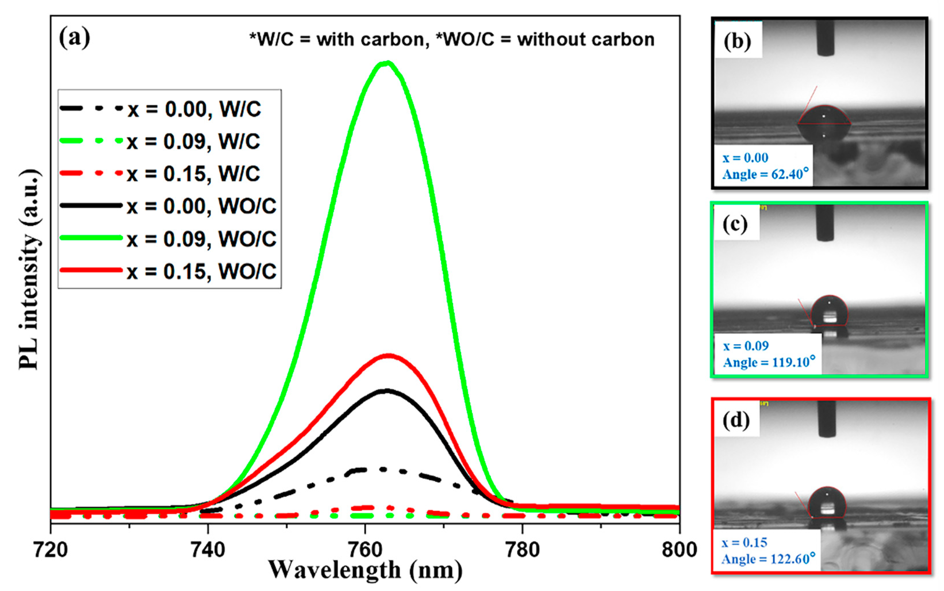
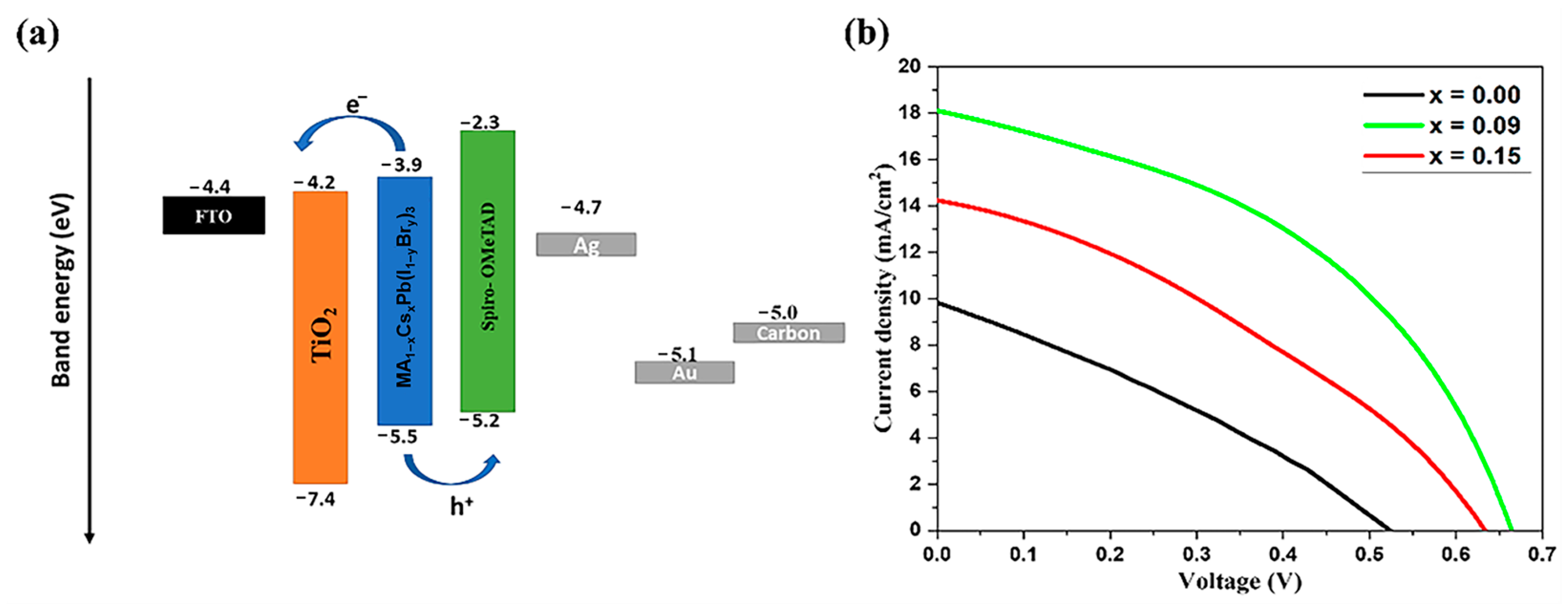
3. Results and Discussion

The effect of variable CsBr-doping concentrations on perovskite films’ crystallinity was investigated by performing XRD analysis (Figure 2a). The typical tetragonal phase of perovskite was identified in all the tested samples. The diffraction peaks were observed at 14.16, 20.06, 23.54, 24.55, 28.50, 31.95, 35.04, and 40.72°, which correspond to the crystal planes 110, 112, 211, 202, 220, 310, 312, and 224, respectively, [33]. Negligible differences were highlighted in the diffraction peaks’ positions of the perovskite films doped with different CsBr concentrations. The 2 possible reasons for this slight shift in position are lattice distortion or a strain in the MAPbI3 perovskite at a low Cs-doping concentration [34]. All the XRD peaks for the films doped with x = 0.09 and 0.15 CsBr were similar to those of the control perovskite film (x = 0.00), and no additional peaks were detected (see Figure 2a), thus showing that the CsBr-doping level in the samples was very low, and there was no further possibility to introduce a new phase at these low doping concentrations. However, the diffraction peaks’ widths displayed a slight difference when the Cs-doping concentration was increased; a reduction in a peak’s width corresponded to an increase in the crystal size and crystallinity and vice versa (Figure 2b,c). The improvement in crystallinity is clearly evident by looking at the intensity change in plane 110 (Figure 2b). Moreover, the peak intensity of the 110 and 220 planes increased significantly for x = 0.09 films, whereas it started decreasing by further increasing the CsBr content (x = 0.15) [35,36].
The full width at half maximum (FWHM), as well as the crystallite size, were calculated for all the investigated perovskite films, and the smallest FWHM value of 0.095 was assessed for the x = 0.09 sample. This small value of FWHM indicates that the perovskite phase exhibits the highest crystallinity in the 110 plane, with the highest peak [37]. Then using the Scherrer formula, the crystal grain size D of perovskite films was calculated according to the diffraction peak observed at 14.16°:
D = 0.9 λ/β cosθ
where λ represents the X-ray wavelength (0.154 nm), β the FWHM of the 110 peak, and θ the Bragg angle [35]. The results of these calculations, shown in Figure 2c, highlight that by increasing the Cs-doping concentration, the crystal size increased up to x = 0.09, and then it started decreasing; as soon as the intensity was improving, the crystallite size was improving; however, when the FWHM started increasing, the crystallite size started decreasing. Perovskite films with a Cs-doping concentration equal to x = 0.15 were additionally fabricated, and it was observed that films turned inhomogeneous as well as rough having low purity and pinholes in higher density, as evident by the SEM and AFM results shown later in the study and in Figure S1, respectively.
The UV–Vis–NIR absorption spectra of all the investigated perovskite films are shown in Figure 3a. In agreement with the XRD patterns presented in Figure 2a, the doping with increasing concentrations of Cs did not affect consistently the shape of the absorption curves in the range of 450 to 790 nm. However, the absorption edge shifted towards shorter wavelengths when the Cs-doping concentration was increased [38]. Using the method described by A.B. Murphy [39], the optical band gap (Eg) values were calculated for all the synthesized perovskite films [40].
The Eg values were found to be similar for all the films; however, a slight increase from the value of 1.57 eV for the undoped film was detected when increasing the concentration of Cs (see Figure 3b–d). Furthermore, the samples doped with x = 0.09 and 0.15 CsBr exhibited Eg values equal to 1.60 and 1.62 eV, respectively, thus implying that the tuning of the Eg can be easily achieved by controlling the CsBr content in the perovskite film (Figure 3b–d). Perovskite materials with a low band gap can absorb lower-energy photons to generate more electron-hole pairs.
The photophysical properties of the MA1−xCsxPb(I1−yBry)3 nanocrystals were evaluated using steady state PL measurements, while the Cs-doping concentration was gradually increased. From the PL results, it can be witnessed that the emission maxima (λem max) of the MA1−xCsxPb(I1−yBry)3 perovskite films can be adjusted in the range of 760 to 765 nm with a fixed excitation peak at 380 nm [41,42]. The PL peak intensity for the control perovskite film was lower in comparison with that of Cs-doped perovskite films. The enhanced PL peak intensity of Cs-doped perovskite films explains the reduction in surface-trap states (which were due to non-radiative recombination) and the enhanced crystallinity (consistent with the SEM results shown later in the study). A larger amount of the Cs-doping concentration (x = 0.15) resulted in a PL intensity decrease [6,43], as shown in Figure 4a.
The Urbach energy (Eu), which is the electronic disorder below the optical band gap, was calculated by linearly fitting ln(α) versus profile using the following relation:
α = α 0 e x p E E u
where α represents the absorption coefficient, α0 a material constant, and E the photon energy [44,45]. This relation was used to obtain further insight into the quality of the perovskite films, after Cs-doping. The Eu value for the control film (x = 0.00) was 216 meV, whereas the samples doped with x = 0.09 and 0.15 Cs concentrations exhibited a lower value of 152 meV and a comparable value of 213 meV, respectively, as shown in Figure 4b–d. The lower Eu value exhibited by the x = 0.09 sample was a clear indication of the trap state density reduction, and these results are in line with the steady state PL measurements shown in Figure 4a. No peak shift was noticeable in the PL spectra [46].
The strength as well as orientation of known chemical bonds were identified by performing FTIR analysis. The purpose was to look for any possible changes in the position of bonds owing to the presence of CsBr in MAPbI3 perovskite films. The FTIR technique is very useful to identify the bonds in complex structure organic molecules such as perovskites, where there may be precise signature peaks due to the presence of external impulses. The FTIR spectra of Cs-doped perovskite films measured at room temperature are shown in Figure 5a. In the literature, for conventional MAPbX3 perovskites, vibrational spectroscopic measurements highlighting reliable peaks for N-H, C-H, and CH3-NH3 have been reported [47]. In this study, 4 prominent peaks at 900, 1500, 3150, and 3180 cm−1 were identified in the control (x = 0.00) perovskite film (see Figure 5a,b). The structure of the peak at 3150 cm−1 was slightly doublet and corresponded to the N-H stretch in the NH3+ ion; moreover, this structure was an indication of a symmetric as well as asymmetric NH3+ stretching combination. The peaks at 1500 and 900 cm−1 were assigned to ammonium bond bending and CH3-NH3, respectively. Interestingly, the peaks remained similar to those of pure MAPbI3 upon increasing the CsBr-doping. However, minor variations were highlighted; in particular, 2 distinct peaks close to 3180 and 3116 cm−1 replaced the peak at 3180 cm−1. These 2 peaks were responsible for minor variations in the structure of CH3-NH3, indicating that the Cs’ presence resulted in local environment changes in the methylammonium group; however, the counter inorganic part stayed stable. As the doping concentration of Cs was further increased, the double peaks at 3180 and 3116 cm−1 remained prominent with the maximum intensity occurring in the x = 0.09 film. The intensity of these 2 peaks showed a slight reduction at x = 0.15, while it was significantly reduced, and it almost vanished if CsBr was further added into the perovskite film. At the x = 0.15 Cs-doping concentration, the peak at 1500 cm−1 narrowly started to increase, whereas no prominent effect was evidenced on the 900 cm−1 peak. Thus, it can be deduced that the presence of Cs above a certain level (x = 0.09) leads to structure percolation resulting in conductivity changes. However, it remains ambiguous whether Cs-doping merely brings changes to the surrounding electronic structure or it enforces the new structure formation [34].
Grain boundaries (GBs), being characterized by the presence of a high number of defects, are mainly responsible for non-radiative recombination and additionally promote trap-assisted charge carrier recombination in perovskite films. In some studies, it was found that the process of ion migration tends to dominate at GBs in MAPbI3-based perovskites rather than in the grain interiors [48]; moreover, the increase in grain size was found to lead to an increase in the activation energy of ionic migration. Several research groups have established that the grain size increase causes a decrease in GBs [49,50,51]. Further confirmation of these results was assessed by performing SEM analysis at the 3 different Cs-doping concentrations of x = 0.00, x = 0.09, and x = 0.15 (see Figure 6a–c). From the SEM results, it can clearly be deduced that there were no visible pinholes, and the grown perovskite films exhibited large grains with full substrate coverage. The film with a Cs-doping concentration equal to x = 0.09 showed minimized GBs and an improved grain size (170 nm) (Figure 6e) as compared to the control (x = 0.00) sample (Figure 6d). Additionally, and as expected, the EDS spectrum of the x = 0.00 sample did not reveal any peak for the Cs+ and Br-, whereas prominent peaks were observed in the EDS spectra of the Cs-doped samples (Figure S2). Interestingly, as shown in Figure 6f, when the Cs-doping concentration was further increased up to x = 0.15, the grain size was slightly decreased, and Cs particles agglomeration could be observed. These agglomeration sites led to an increase in the surface roughness, as clearly evident from the AFM analysis results shown in Figure S1: when the concentration of Cs was low, the surface roughness and root mean square roughness (Rrms) were high; however, as soon as the doping concentration of Cs was increased, this Rrms value started decreasing from 60 nm for the x = 0.00 sample to 10 nm for the doped sample (x = 0.09). This simply means that with increasing the doping concentration, the GBs started increasing and, overall, a smoother perovskite absorber layer was produced. With a smaller number of GBs, the charge transfer was enhanced, and as a result, cell performance was increased. However, after a certain level of the Cs-doping concentration (x = 0.15), the agglomeration started, thus leading to the increase in the Rrms value (17 nm) and to the deterioration of the film’s quality.
PL characterization was performed to check the charge carrier transfer and extraction behavior at the interface of the perovskite/carbon electrode at different Cs-doping concentrations. The PL spectra showed a perovskite luminescence peak at 760 nm, as demonstrated in Figure 7a. The substantial quenching of PL in the presence of the carbon electrode indicated the charge transfer between the perovskite film and the CE [52]. The interesting fact to be noted is that an even more extensive quenching of PL occurred when the doping concentration was increased up to x = 0.09, because at this doping concentration the perovskite absorber layer exhibited fewer trap defect states and fewer GBs. However, when the doping concentration was further increased (x = 0.15), the PL peak started to increase, which means that the presence of trap defect states was increasing with the agglomeration at the surface of the film, the charge carrier transfer was hindered by the presence of this poor quality of the film, and the overall efficiency and stability of the device were compromised [52].
The water contact angle was measured to further investigate the role of carbon CE in increasing the stability of the PSCs [53]. More specifically, the water contact angle was measured on both the (i) Cs-doped absorber layers and (ii) Cs-doped absorber layers with carbon CE, to check the effect of the humidity on the Cs-doping in the presence and in the absence of the carbon CE. As demonstrated in Figure S3a–c, as the Cs-doping concentration was increased the water contact angle was additionally increased due to the more compact film morphology. On the other hand, when the carbon was deposited on the perovskite films, they became more hydrophobic, as shown in Figure 7b–d. The superior resistance against moisture offered by the top carbon/perovskite layer as a consequence of its compact structure and large water contact angle is responsible for the superior stability of the cell [53].
The C-PSCs energy level diagram has been schematized in Figure 8a [54,55,56]. The electrons injection into the TiO2 conduction band was efficient, due to the proper alignment between the ambipolar perovskite and the meso-TiO2 energy levels, while holes could be collected at the carbon CE and then travel through the external circuit. The photocurrent density–voltage (J-V) curves of the PSCs assembled with undoped and Cs-doped perovskite films as the absorber layer and carbon as the CE are reported in Figure 8b. The curves were taken in air mass (AM) 1.5 1-sun (100 mW/cm2) illumination conditions. The output electrical parameters of the solar devices are detailed in Table 1. The charge transport is extremely linked to the interfacial contact between the CE and the perovskite film. The poor interfacial contact between the perovskite film and the graphite flakes in the case of the cells with CE was the reason behind their poorest performance [57].
The devices in this study were fabricated with architecture consisting of FTO/c-TiO2/meso-TiO2/MA1−xCsxPb(I1−yBry)3/carbon (x = 0.00, 0.09, and 0.15). The PCE, Voc, FF, and Jsc of the cell fabricated with the control perovskite film (x = 0.00) were 1.55%, 0.530 V, 0.29, and 9.56 mA/cm2, respectively. The highest PCE value of 5.27% was achieved at an x = 0.09 Cs-doping concentration; interestingly, when the Cs-doping concentration was increased from x = 0.09 to x = 0.15, the PCE decreased to 3.09%. The decreased PCE of the device at x = 0.15 was attributed to a lower open-circuit voltage and short-circuit current density, due to smaller grain sizes. Upon increasing the doping level of Cs from x = 0.00 to x = 0.09, the corresponding increase in Voc, Jsc, FF, and PCE was from 0.530 to 0.659 V, 9.56 to 18.05 mA/cm2, 0.29 to 0.44, and 1.55 to 5.27%, respectively. Both Figure 2a (XRD) and Figure 6a–c (SEM) highlight that the crystal grains grew much larger when the perovskite film was doped with Cs. The larger the grain’s size, the smaller will be the area occupied by GBs, thus resulting in fewer defects and recombination losses of photogenerated carriers contributing to improved electronic output parameters. Interesting studies in the literature have shown that the grains grow even larger with Br- instead of Cs+-doping [58,59]; that is why the replacement of I with Br is worth considering in MAPbI3 to help perovskite crystal grains grow bigger. Moreover, another key factor contributing to an increase in open-circuit voltage is the blue shifting of the perovskite band gap upon doping with CsBr, as reported in Figure 3a. These findings proved the fact that the broadening of a plain perovskite thin film’s band gap can take place due to doping with Br or Cs+ [17,34,58]. The improvement in FF after doping with CsBr can be attributed to the enhanced charge transport induced by replacing I with Br [60]. On increasing the doping level of CsBr from x = 0.09 to x = 0.15, the Voc, Jsc, and FF decreased, respectively, from 0.659 V, 18.05 mA/cm2, and 0.44 to 0.639 V, 14.13 mA/cm2, and 0.30. Both the XRD and SEM results showed that the increased GBs by Cs-doping (see Figure 2a and Figure 6a–c) may increase the charge carrier recombination probability and, therefore, attenuate the photovoltaic current density [33,61]. The smoothness of the perovskite absorber layer was reduced with increasing the CsBr-doping concentration, due to the agglomeration of the Cs+ and to the halide segregation. Therefore, there was weak interfacial contact between the perovskite and carbon layers due to which the shunt resistance and series resistance were increased, and there was an additional drop in the Jsc and Voc at x = 0.15.

4. Conclusions

In this work, the effect of different Cs-doping concentrations on the morphological, structural, optical, spectroscopic, and luminescent properties of perovskite absorber layers was thoroughly investigated. The crystallization rate was found to be accelerated upon cesium’s introduction into the precursor, resulting in larger grain size and fewer GBs in the film. Consequently, the defects originating from ion migration at the GBs were suppressed. Moreover, the defect density of states was reduced as evident from the PL spectra. The fabrication of PSCs was carried out in a dry glove box by using carbon as the CE, after successfully optimizing the CsBr-concentration in the perovskite absorber layer at x = 0.09. The high charge carrier mobility of the carbon CE enhanced the hole extraction from perovskite film and decreased the recombination in the device, due to the inertness of the carbon electrode to the ion migration originating from the perovskite film. The best performing PSC was assembled with the perovskite film doped with a Cs-doping level of x = 0.09 and showed a PCE of 5.27%, which is consistently higher than the 1.55% exhibited by the solar device based on the control (x = 0.00) perovskite film. Additionally, the hydrophobic and dense carbon CE layer provided enhanced resistance to perovskite film against ambient moisture. This technique proposes a promising pathway for reducing the fabrication cost of PSCs, by exploring low-cost carbon-based materials and making the PSCs’ commercialization easier.

Supplementary Materials

The following supporting information can be downloaded at the subsequent link: https://www.mdpi.com/article/10.3390/en16124748/s1; Figure S1: AFM 3D images and topographic maps of the perovskite films at different CsBr-doping concentrations: (a) x = 0.00, (b) x = 0.09, and (c) x = 0.15; Figure S2: EDS mapping of the perovskite films doped with different CsBr concentrations: (a) x = 0.00, (b) x = 0.09, and (c) x = 0.15; and Figure S3: water contact angle of perovskite absorber layers doped with the 3 different CsBr-doping concentrations of (a) x = 0.00, (b) x = 0.09, and (c) x = 0.15 in the absence of carbon CE.

Author Contributions

Conceptualization, T.Y.; methodology, T.Y.; formal analysis, T.Y., M.A.T. and D.P.; investigation, T.Y.; data curation, A.S.; writing—original draft preparation, T.Y.; writing—review and editing, N.S., A.S., N.H., Z.S.K., S.J., M.I.S. and D.P.; supervision, N.S. All authors have read and agreed to the published version of the manuscript.

Funding

This research was funded by the HIGHER EDUCATION COMMISSION (HEC), Pakistan, grant number NRPU-6046.

Data Availability Statement

Data are available on request due to the restrictions of privacy.

Conflicts of Interest

The authors declare no conflict of interest.

References

  1. Ali, H.M.; Reda, S.M.; Ali, A.I.; Mousa, M.A. A quick peek at solar cells and a closer insight at perovskite solar cells. Egypt. J. Pet. 2021, 30, 53–63. [Google Scholar] [CrossRef]
  2. Qiang, Y.; Xie, Y.; Qi, Y.; Wei, P.; Shi, H.; Geng, C.; Liu, H. Enhanced performance of carbon-based perovskite solar cells with a Li+-doped SnO2 electron transport layer and Al2O3 scaffold layer. Sol. Energy 2020, 201, 523–529. [Google Scholar] [CrossRef]
  3. Jin, J.; Yang, M.; Deng, W.; Xin, J.; Tai, Q.; Qian, J.; Dong, B.; Li, W.; Wang, J.; Li, J. Highly efficient and stable carbon-based perovskite solar cells with the polymer hole transport layer. Sol. Energy 2021, 220, 491–497. [Google Scholar] [CrossRef]
  4. Keremane, K.S.; Prathapani, S.; Haur, L.J.; Bahulayan, D.; Adhikari, A.V.; Priyadarshi, A.; Mhaisalkar, S.G. Solvent selection for highly reproducible carbon-based mixed-cation hybrid lead halide perovskite solar cells via adduct approach. Sol. Energy 2020, 199, 761–771. [Google Scholar] [CrossRef]
  5. Maram, D.K.; Habibiyan, H.; Ghafoorifard, H.; Shekoofa, O. Analysis of Optimum Copper Oxide Hole Transporting Layer for Perovskite Solar Cells. In Proceedings of the 27th Iranian Conference on Electrical Engineering (ICEE), Yazd, Iran, 30 April–2 May 2019. [Google Scholar]
  6. Zhao, X.-C.; Wu, D.-X.; Yang, L.-J.; Tang, J.; Yue, G.-Z.; Yang, P. Cesium-containing methylammonium lead iodide light absorber for planar perovskite solar cells. J. Nanosci. Nanotechnol. 2020, 20, 1008–1012. [Google Scholar] [CrossRef]
  7. Maram, D.K.; Haghighi, M.; Shekoofa, O.; Habibiyan, H.; Ghafoorifard, H. A modeling study on utilizing ultra-thin inorganic HTLs in inverted p–n homojunction perovskite solar cells. Sol. Energy 2021, 213, 1–12. [Google Scholar] [CrossRef]
  8. Best Research-Cell Efficiency Chart. Available online: https://www.nrel.gov/pv/cell-efficiency.html (accessed on 4 May 2023).
  9. Han, Q.; Yang, S.; Wang, L.; Yu, F.; Zhang, C.; Wu, M.; Ma, T. The sulfur-rich small molecule boosts the efficiency of carbon-based CsPbI2Br perovskite solar cells to approaching 14%. Sol. Energy 2021, 216, 351–357. [Google Scholar] [CrossRef]
  10. Nkele, A.C.; Nwanya, A.C.; Shinde, N.M.; Ezugwu, S.; Maaza, M.; Shaikh, J.S.; Ezema, F.I. The use of nickel oxide as a hole transport material in perovskite solar cell configuration: Achieving a high performance and stable device. Int. J. Energy Res. 2020, 44, 9839–9863. [Google Scholar] [CrossRef]
  11. Wang, Y.; Bai, S.; Cheng, L.; Wang, N.; Wang, J.; Gao, F.; Huang, W. High-efficiency flexible solar cells based on organometal halide perovskites. Adv. Mater. 2016, 28, 4532–4540. [Google Scholar] [CrossRef]
  12. Nkele, A.C.; Ike, I.S.; Ezugwu, S.; Maaza, M.; Ezema, F.I. An overview of the mathematical modelling of perovskite solar cells towards achieving highly efficient perovskite devices. Int. J. Energy Res. 2021, 45, 1496–1516. [Google Scholar] [CrossRef]
  13. Noh, J.H.; Im, S.H.; Heo, J.H.; Mandal, T.N.; Seok, S.I. Chemical management for colorful, efficient, and stable inorganic–organic hybrid nanostructured solar cells. Nano Lett. 2013, 13, 1764–1769. [Google Scholar] [CrossRef]
  14. Wei, Y.; Li, W.; Xiang, S.; Liu, J.; Liu, H.; Zhu, L.; Chen, H. Precursor effects on methylamine gas-induced CH3NH3PbI3 films for stable carbon-based perovskite solar cells. Sol. Energy 2018, 174, 139–148. [Google Scholar] [CrossRef]
  15. Li, Z.; Yang, M.; Park, J.-S.; Wei, S.-H.; Berry, J.J.; Zhu, K. Stabilizing perovskite structures by tuning tolerance factor: Formation of formamidinium and cesium lead iodide solid-state alloys. Chem. Mater. 2016, 28, 284–292. [Google Scholar] [CrossRef]
  16. Wang, B.; Novendra, N.; Navrotsky, A. Energetics, structures, and phase transitions of cubic and orthorhombic cesium lead iodide (CsPbI3) polymorphs. J. Am. Chem. Soc. 2019, 141, 14501–14504. [Google Scholar] [CrossRef]
  17. Choi, H.; Jeong, J.; Kim, H.-B.; Kim, S.; Walker, B.; Kim, G.-H.; Kim, J.Y. Cesium-doped methylammonium lead iodide perovskite light absorber for hybrid solar cells. Nano Energy 2014, 7, 80–85. [Google Scholar] [CrossRef]
  18. Zhao, F.; Guo, Y.; Wang, X.; Tao, J.; Jiang, J.; Hu, Z.; Chu, J. Enhanced performance of carbon-based planar CsPbBr3 perovskite solar cells with room-temperature sputtered Nb2O5 electron transport layer. Sol. Energy 2019, 191, 263–271. [Google Scholar] [CrossRef]
  19. Saliba, M.; Matsui, T.; Seo, J.-Y.; Domanski, K.; Correa-Baena, J.-P.; Nazeeruddin, M.K.; Zakeeruddin, S.M.; Tress, W.; Abate, A.; Hagfeldt, A.; et al. Cesium-containing triple cation perovskite solar cells: Improved stability, reproducibility and high efficiency. Energy Environ. Sci. 2016, 9, 1989–1997. [Google Scholar] [CrossRef] [Green Version]
  20. Berhe, T.A.; Su, W.-N.; Chen, C.-H.; Pan, C.-J.; Cheng, J.-H.; Chen, H.-M.; Tsai, M.-C.; Chen, L.-Y.; Dubale, A.A.; Hwang, B.-J. Organometal halide perovskite solar cells: Degradation and stability. Energy Environ. Sci. 2016, 9, 323–356. [Google Scholar] [CrossRef]
  21. Wang, J.; Chen, X.; Jiang, F.; Luo, Q.; Zhang, L.; Tan, M.; Xie, M.; Li, Y.-Q.; Zhou, Y.; Su, W.; et al. Electrochemical corrosion of Ag electrode in the silver grid electrode-based flexible perovskite solar cells and the suppression method. Sol. RRL 2018, 2, 1800118. [Google Scholar] [CrossRef]
  22. Grancini, G.; Roldán-Carmona, C.; Zimmermann, I.; Mosconi, E.; Lee, X.; Martineau, D.; Narbey, S.; Oswald, F.; De Angelis, F.; Graetzel, M.; et al. One-Year stable perovskite solar cells by 2D/3D interface engineering. Nat. Commun. 2017, 8, 15684. [Google Scholar] [CrossRef] [Green Version]
  23. Bidikoudi, M.; Simal, C.; Stathatos, E. Low-toxicity perovskite applications in carbon electrode perovskite solar cells—A review. Electronics 2021, 10, 1145. [Google Scholar] [CrossRef]
  24. Bogachuk, D.; Zouhair, S.; Wojciechowski, K.; Yang, B.; Babu, V.; Wagner, L.; Xu, B.; Lim, J.; Mastroianni, S.; Pettersson, H.; et al. Low-temperature carbon-based electrodes in perovskite solar cells. Energy Environ. Sci. 2020, 13, 3880–3916. [Google Scholar] [CrossRef]
  25. Que, M.; Zhang, B.; Chen, J.; Yin, X.; Yun, S. Carbon-based electrodes for perovskite solar cells. Mater. Adv. 2021, 2, 5560–5579. [Google Scholar] [CrossRef]
  26. Bashir, A.; Haur, J.H.; Shukla, S.; Gupta, D.; Baikie, T.; Chakraborty, S.; Patidar, R.; Bruno, A.; Mhaisalkar, S.; Akhter, Z. Cu-doped nickel oxide interface layer with nanoscale thickness for efficient and highly stable printable carbon-based perovskite solar cell. Sol. Energy 2019, 182, 225–236. [Google Scholar] [CrossRef]
  27. Zhang, H.; Xiao, J.; Shi, J.; Su, H.; Luo, Y.; Li, D.; Wu, H.; Cheng, Y.-B.; Meng, Q. Self-adhesive macroporous carbon electrodes for efficient and stable perovskite solar cells. Adv. Funct. Mater. 2018, 28, 1802985. [Google Scholar] [CrossRef]
  28. Ku, Z.; Rong, Y.; Xu, M.; Liu, T.; Han, H. Full printable processed mesoscopic CH3NH3PbI3/TiO2 heterojunction solar cells with carbon counter electrode. Sci. Rep. 2013, 3, 3132. [Google Scholar] [CrossRef] [Green Version]
  29. Mei, A.; Li, X.; Liu, L.; Ku, Z.; Liu, T.; Rong, Y.; Xu, M.; Hu, M.; Chen, J.; Yang, Y.; et al. A hole-conductor–free, fully printable mesoscopic perovskite solar cell with high stability. Science 2014, 345, 295–298. [Google Scholar] [CrossRef]
  30. Lyu, B.; Yang, L.; Luo, Y.; Zhang, X.; Zhang, J. Counter electrodes for perovskite solar cells: Materials, interfaces and device stability. J. Mater. Chem. C 2022, 10, 10775–10798. [Google Scholar] [CrossRef]
  31. Kartikay, P.; Yella, A.; Mallick, S. Binder-solvent effects on low temperature-processed carbon-based, hole-transport layer free perovskite solar cells. Mater. Chem. Phys. 2020, 256, 123594. [Google Scholar] [CrossRef]
  32. Vijayaraghavan, S.N.; Wall, J.; Li, L.; Xing, G.; Zhang, Q.; Yan, F. Low-temperature processed highly efficient hole transport layer free carbon-based planar perovskite solar cells with SnO2 quantum dot electron transport layer. Mater. Today Phys. 2020, 13, 100204. [Google Scholar] [CrossRef]
  33. Fan, Y.; Qin, H.; Ye, W.; Liu, M.; Huang, F.; Zhong, D. Improving the stability of methylammonium lead iodide perovskite solar cells by cesium doping. Thin Solid Films 2018, 667, 40–47. [Google Scholar] [CrossRef]
  34. Murugadoss, G.; Thangamuthu, R.; Vijayaraghavan, S.; Kanda, H.; Ito, S. Caesium—Methyl ammonium mixed-cation lead iodide perovskite crystals: Analysis and application for perovskite solar cells. Electrochim. Acta 2017, 257, 267–280. [Google Scholar] [CrossRef]
  35. Zhang, L.-Y.; Zhang, Y.; Guan, W.-B.; Wang, K.-F.; Cheng, Z.-X.; Wang, Y.-X. Large enhanced conversion efficiency of perovskite solar cells by CsBr doping. J. Mater. Sci. 2017, 52, 13203–13211. [Google Scholar] [CrossRef]
  36. Zhao, Y.; Zhu, K. Charge transport and recombination in perovskite (CH3NH3)PbI3 sensitized TiO2 solar cells. J. Phys. Chem. Lett. 2013, 4, 2880–2884. [Google Scholar] [CrossRef]
  37. Singh, T.; Miyasaka, T. Stabilizing the efficiency beyond 20% with a mixed cation perovskite solar cell fabricated in ambient air under controlled humidity. Adv. Energy Mater. 2018, 8, 1700677. [Google Scholar] [CrossRef]
  38. Zou, Y.; Yuan, S.; Buyruk, A.; Eichhorn, J.; Yin, S.; Reus, M.A.; Xiao, T.; Pratap, S.; Liang, S.; Weindl, C.L.; et al. The influence of CsBr on crystal orientation and optoelectronic properties of MAPbI3-based solar cells. ACS Appl. Mater. Interfaces 2022, 14, 2958–2967. [Google Scholar] [CrossRef]
  39. Murphy, A.B. Band-gap determination from diffuse reflectance measurements of semiconductor films, and application to photoelectrochemical water-splitting. Sol. Energy Mater. Sol. Cells 2007, 91, 1326–1337. [Google Scholar] [CrossRef]
  40. Gordillo, G.; Luis, L.C.; Buitrago, J.P.; Reinoso, M.A. Influence of the Concentration of Cs on the Properties of Thin Films of CsXMA(1-X)PbI3 to be used as Active Layer in Hybrid Solar Cells. In Proceedings of the 7th World Conference on Photovoltaic Energy Conversion (WCPEC), Waikoloa, HI, USA, 10–15 June 2018. [Google Scholar]
  41. Premkumar, S.; Kundu, K.; Umapathy, S. Impact of cesium in methylammonium lead bromide perovskites: Insights into the microstructures, stability and photophysical properties. Nanoscale 2019, 11, 10292–10305. [Google Scholar] [CrossRef]
  42. Ng, C.H.; Ripolles, T.S.; Hamada, K.; Teo, S.H.; Lim, H.N.; Bisquert, J.; Hayase, S. Tunable open circuit voltage by engineering inorganic cesium lead bromide/iodide perovskite solar cells. Sci. Rep. 2018, 8, 2482. [Google Scholar] [CrossRef] [Green Version]
  43. Bahtiar, A.; Yazibarahmah, R.; Aprilia, A.; Hidayat, D. Improved the performance and stability at high humidity of perovskite solar cells by mixed cesium-metylammonium cations. Key Eng. Mater. 2020, 860, 9–14. [Google Scholar] [CrossRef]
  44. Zhang, Y.; Wu, C.; Wang, D.; Zhang, Z.; Qi, X.; Zhu, N.; Liu, G.; Li, X.; Hu, H.; Chen, Z.; et al. High efficiency (16.37%) of cesium bromide—Passivated all-inorganic CsPbI2Br perovskite solar cells. Sol. RRL 2019, 3, 1900254. [Google Scholar] [CrossRef]
  45. Ledinsky, M.; Schönfeldová, T.; Holovský, J.; Aydin, E.; Hájková, Z.; Landová, L.; Neyková, N.; Fejfar, A.; De Wolf, S. Temperature dependence of the Urbach energy in lead iodide perovskites. J. Phys. Chem. Lett. 2019, 10, 1368–1373. [Google Scholar] [CrossRef] [PubMed] [Green Version]
  46. Ghimire, N.; Bobba, R.S.; Gurung, A.; Reza, K.M.; Laskar, M.A.R.; Lamsal, B.S.; Emshadi, K.; Pathak, R.; Afroz, M.A.; Chowdhury, A.H.; et al. Mitigating open-circuit voltage loss in Pb–Sn low-bandgap perovskite solar cells via additive engineering. ACS Appl. Energy Mater. 2021, 4, 1731–1742. [Google Scholar] [CrossRef]
  47. Hou, X.; Huang, S.; Ou-Yang, W.; Pan, L.; Sun, Z.; Chen, X. Constructing efficient and stable perovskite solar cells via interconnecting perovskite grains. ACS Appl. Mater. Interfaces 2017, 9, 35200–35208. [Google Scholar] [CrossRef]
  48. Xing, J.; Wang, Q.; Dong, Q.; Yuan, Y.; Fang, Y.; Huang, J. Ultrafast ion migration in hybrid perovskite polycrystalline thin films under light and suppression in single crystals. Phys. Chem. Chem. Phys. 2016, 18, 30484–30490. [Google Scholar] [CrossRef]
  49. Yang, B.; Brown, C.C.; Huang, J.; Collins, L.; Sang, X.; Unocic, R.R.; Jesse, S.; Kalinin, S.V.; Belianinov, A.; Jakowski, J.; et al. Enhancing ion migration in grain boundaries of hybrid organic–inorganic perovskites by chlorine. Adv. Funct. Mater. 2017, 27, 1700749. [Google Scholar] [CrossRef]
  50. Hoque, M.N.F.; He, R.; Warzywoda, J.; Fan, Z. Effects of moisture-based grain boundary passivation on cell performance and ionic migration in organic–inorganic halide perovskite solar cells. ACS Appl. Mater. Interfaces 2018, 10, 30322–30329. [Google Scholar] [CrossRef]
  51. Singh, R.; Sandhu, S.; Yadav, H.; Lee, J.-J. Stable triple-cation (Cs+–MA+–FA+) perovskite powder formation under ambient conditions for hysteresis-free high-efficiency solar cells. ACS Appl. Mater. Interfaces 2019, 11, 29941–29949. [Google Scholar] [CrossRef]
  52. Nouri, E.; Mohammadi, M.R.; Lianos, P. Construction of perovskite solar cells using inorganic hole-extracting components. ACS Omega 2018, 3, 46–54. [Google Scholar] [CrossRef]
  53. Zhang, Y.; Wang, J.; Liu, X.; Li, W.; Huang, F.; Peng, Y.; Zhong, J.; Cheng, Y.; Ku, Z. Enhancing the performance and stability of carbon-based perovskite solar cells by the cold isostatic pressing method. RSC Adv. 2017, 7, 48958–48961. [Google Scholar] [CrossRef] [Green Version]
  54. Mahmood, K.; Sarwar, S.; Mehran, M.T. Current status of electron transport layers in perovskite solar cells: Materials and properties. RSC Adv. 2017, 7, 17044–17062. [Google Scholar] [CrossRef] [Green Version]
  55. Elumalai, N.K.; Mahmud, M.A.; Wang, D.; Uddin, A. Perovskite solar cells: Progress and advancements. Energies 2016, 9, 861. [Google Scholar] [CrossRef] [Green Version]
  56. Chen, H.; Yang, S. Carbon-based perovskite solar cells without hole transport materials: The front runner to the market? Adv. Mater. 2017, 29, 1603994. [Google Scholar] [CrossRef]
  57. Wei, H.; Xiao, J.; Yang, Y.; Lv, S.; Shi, J.; Xu, X.; Dong, J.; Luo, Y.; Li, D.; Meng, Q. Free-standing flexible carbon electrode for highly efficient hole-conductor-free perovskite solar cells. Carbon 2015, 93, 861–868. [Google Scholar] [CrossRef]
  58. Zhu, W.; Bao, C.; Li, F.; Yu, T.; Gao, H.; Yi, Y.; Yang, J.; Fu, G.; Zhou, X.; Zou, Z. A halide exchange engineering for CH3NH3PbI3−xBrx perovskite solar cells with high performance and stability. Nano Energy 2016, 19, 17–26. [Google Scholar] [CrossRef]
  59. Niemann, R.G.; Gouda, L.; Hu, J.; Tirosh, S.; Gottesman, R.; Cameron, P.J.; Zaban, A. Cs+ incorporation into CH3NH3PbI3 perovskite: Substitution limit and stability enhancement. J. Mater. Chem. A 2016, 4, 17819–17827. [Google Scholar] [CrossRef] [Green Version]
  60. Atourki, L.; Vega, E.; Marí, B.; Mollar, M.; Ait Ahsaine, H.; Bouabid, K.; Ihlal, A. Role of the chemical substitution on the structural and luminescence properties of the mixed halide perovskite thin MAPbI3−xBrx (0 ≤ x ≤ 1) films. Appl. Surf. Sci. 2016, 371, 112–117. [Google Scholar] [CrossRef]
  61. Niu, G.; Li, W.; Li, J.; Liang, X.; Wang, L. Enhancement of thermal stability for perovskite solar cells through cesium doping. RSC Adv. 2017, 7, 17473–17479. [Google Scholar] [CrossRef] [Green Version]
Figure 1. Step-by-step methodology for the assembling of PSCs.
Energies 16 04748 g001
Figure 2. (a) XRD patterns of the perovskite films doped with different CsBr-concentrations; (b) zoom-up of the XRD peak centered at 14.16°; and (c) crystallite size of the perovskite films as a function of the CsBr-doping concentration.
Energies 16 04748 g002
Figure 3. Absorption curves (a) and Tauc plots (bd) of the perovskite films doped with the 3 different CsBr-doping concentrations of x = 0.00, 0.09, and 0.15.
Energies 16 04748 g003
Figure 4. (a) PL spectra of perovskite absorber layers at different doping concentrations of CsBr. Estimation of Urbach energy for the (b) x = 0.00, (c) x = 0.09, and (d) x = 0.15 perovskite films.
Energies 16 04748 g004
Figure 5. (a) FTIR spectra of the perovskite films doped with the 3 different CsBr-concentrations of x = 0.00, x = 0.09, and x = 0.15 and (b) zoom-up of the peak centered at 3180 cm−1 to check the effect of the Cs-doping on the perovskite structure.
Energies 16 04748 g005
Figure 6. Top view SEM images of the perovskite films at different CsBr-doping concentrations: (a) x = 0.00, (b) x = 0.09, and (c) x = 0.15; (df) grain size distribution of the perovskite films at different CsBr-doping concentrations.
Energies 16 04748 g006
Figure 7. (a) PL spectra of perovskite absorber layers at different doping concentrations of CsBr with and without carbon; (bd) water contact angle of perovskite absorber layers doped with the 3 different CsBr-doping concentrations of x = 0.00, x = 0.09, and x = 0.15 in the presence of carbon CE.
Energies 16 04748 g007
Figure 8. (a) Energy level diagram of C-PSCs [55,56] and (b) J-V curves of PSCs employing undoped and Cs-doped perovskite absorber layers and carbon CE.
Energies 16 04748 g008
Table 1. Photovoltaic parameters of PSCs based on undoped and Cs-doped perovskite absorber layers and carbon CE. Vmp, Imp, Voc, Jsc, and FF represent the voltage at maximum power, the current at maximum power, the open-circuit voltage, the short-circuit current density, and the fill factor, respectively.
xVmp (V)Imp (A)Voc (V)Jsc (mA/cm2)FFPCE (%)
0.000.3065.070.5309.560.291.55
0.090.54211.130.65918.050.445.27
0.150.3688.410.63914.130.303.09
Disclaimer/Publisher’s Note: The statements, opinions and data contained in all publications are solely those of the individual author(s) and contributor(s) and not of MDPI and/or the editor(s). MDPI and/or the editor(s) disclaim responsibility for any injury to people or property resulting from any ideas, methods, instructions or products referred to in the content.

