Article

A Compact High-Stability Nanosecond Pulse Test System Using Corona-Stabilized Switch and Coaxial Resistance Divider

State Key Laboratory of Electrical Insulation and Power Equipment, Xi’an Jiaotong University, Xi’an 710049, China
*
Author to whom correspondence should be addressed.
Energies 2023, 16(11), 4534; https://doi.org/10.3390/en16114534
Submission received: 20 April 2023 / Revised: 28 May 2023 / Accepted: 29 May 2023 / Published: 5 June 2023
(This article belongs to the Special Issue Advances in Pulsed Power Technologies)

Abstract

:
Due to the lack of a standard nanosecond high-voltage pulse generator for sensor calibration, a high-stability nanosecond high-voltage pulse test system was developed in terms of circuit analysis, structural design, and performance test. By establishing the equivalent circuit model of the nanosecond pulse generator, the circuit component parameters of the five-stage Marx loop and the one-stage compression steepening unit were simulated. The influence of the action performance of the steepening gap on the characteristics of output nanosecond pulse was analyzed. The nanosecond pulse test system was established through the structural design of the nanosecond pulse-generating circuit, the development of a high-performance corona-stabilized switch, and the measurement of a fast-response resistance divider made of metal oxide thin-film resistors. The nanosecond pulse test system has the capability to output a double exponential nanosecond pulse voltages in the amplitude range of 10–60 kV with a rise time of 2.3 ± 0.5 ns and a half-peak time of 23 ± 5 ns. In addition, the output pulse voltage has a high consistency and stability in the full amplitude range. The maximum relative standard deviation of the peak value is 1.517%, and the relative standard uncertainty is less than 5‰.

1. Introduction

A high-altitude electromagnetic pulse (HEMP) has a high peak field strength, rapid rise time, tremendous energy, and a wide application range. A severe threat to highly integrated, ultra-large-scale integrated circuits and other electronic devices is posed by the electromagnetic field that results from this interaction with electronic systems, which produces catastrophic overvoltage and current surges. Conducting HEMP simulation tests and observing the operating state of electronic information equipment in the complex electromagnetic environment is an important method to assess the anti-EMP interference capability of electronic equipment and integrated circuits. HEMP test systems are the core equipment for the HEMP electromagnetic effects and protection performance testing of electronic systems. To verify the survivability of military and civilian electronic products and electrical equipment in complex electromagnetic environments, researchers have developed some HEMP simulation devices and EMP simulation test standards in various countries.
Marx circuits are widely used in HEMP simulation devices due to their simple structure, reliable performance, and easy adjustment. Based on the integrated design method of switches, capacitors, and insulating cavities, researchers have developed a variety of compact Marx generators for studies in pulsed laser, high-frequency characteristic detection of GIS device, plasma heating, bioelectromagnetic, etc. [1,2,3,4]. As the demand for high-intensity fast-front nanosecond (ns) electromagnetic pulse tests increase, the inductance of the Marx generator can no longer meet the rise time requirement. Thus, Marx-loop-based pulse steepening technology has been strongly developed. The three-stage pulse compression designed by C. Gilman et al. [5] is achieved by a 34-stage Marx generator, a transfer circuit consisting of a transfer capacitor, a transfer switch, a peaking capacitor, and an output switch. Based on pulse compression technology, the FEMP-2000 Pulser can generate high-voltage electromagnetic pulses with a 2 MV amplitude and a sub-ns rise time. Drawing on the design structure of the FEMP-2000 Pulser’s capacitors and switches, V. Bailey et al. [6] of L-3 Communications Pulse Sciences completed the development of a 6-MV biconic pulse generator using a low-inductance Marx generator and the two-stage pulse compression technology of the peaking capacitor. This multi-stage Marx circuitry can generate a primary pulse, followed by one or more stages of pulse compression for fast-rising nanosecond electromagnetic pulse formation. It is used in a number of HEMP generators in the range of several tens of kV to several MV magnitudes.
Nanosecond pulse sensors are essential in HEMP test systems for precisely acquiring waveform information and efficiently assessing EMP generator performance. Nanosecond double exponential pulses place extremely exacting demands on the measuring system due to their steep rising edges and narrow pulse half-widths. However, the sensors are rarely mentioned in the published HEMP simulator studies. Some researchers uses specially designed voltage sensors for specific nanosecond pulse measurements [5,7,8]. However, practitioners have struggled with the challenge of calibrating ns pulse sensors, which is often conducted by comparing with available commercial probes, such as P6015 and P6139A [9,10,11], or standard attenuators [12,13,14] at low-intensity pulses. In this case, the suitability of the sensor for measuring nanosecond pulses is governed by the response performance of the standard sensor selected in the calibration. However, the sensing factors of these “standard” sensors are usually determined under microsecond pulse conditions, and their traceability in a nanosecond pulse environment is frequently not guaranteed. Due to the difficulties in the development of high-stability nanosecond pulse generators and the challenge in sensor technologies including electromagnetic compatibility and calibration methods, national metrology institutes are not yet able to calibrate fast-rising, high-amplitude nanosecond pulse test systems and sensors [15]. Therefore, the development of a highly stable nanosecond pulse test system is the foundation for improving the calibration accuracy of sensors, as well as the key for evaluating the output performance and stability of nanosecond electromagnetic pulse generator.
Switch technology governs the waveform quality and output stability in nanosecond pulse-generating circuits. Solid-state semiconductor switches have been used successfully in kHz repetition frequency nanosecond pulse sources due to their benefits of compact size, low weight, and high operating frequency. Yan et al. [16] use the external magnetic field to drive a wet reed relay to generate the square wave pulse with a rise time in the range of ns and an amplitude of 500 V. However, because of the modest power capacity of semiconductor devices, the majority of the output pulse voltage intensity is in the range of several kV. It is challenging to directly generate high-amplitude pulse voltages with a semiconductor-based circuit. Considering the operating voltage and current requirements of switches in HEMP simulators, gas spark gaps are adopted in some nanosecond pulse generators [5,6,8,17,18,19,20,21]. The FEMP-2000 [5] and HEREMP [6] from Centre d’Etudes de Gramat, France, use three spark gaps in series and control the switch operating voltage by adjusting the SF6 gas pressure. Gubanov et al. [7] use a high voltage air gap switch with N2 gas circulation, capable of generating a maximum charging voltage of 450 kV repetitive frequency pulses. The switching consistency has a significant impact on the output waveform quality. Ordinary gas switches usually lead to poor waveform stability due to their high discharge dispersion. Therefore, an advanced output switch with stable conduction delay and small jitter needs to be developed to prevent severe waveform distortion and output efficiency degradation during pulse compression. In addition, the evaluation of the performance of the developed pulsed power has focused on the output pulse waveform parameters, while the output stability of the pulse source lacks test results, and only a few studies have focused on the measurement uncertainty of the nanosecond pulse sensor [22].
This paper focuses on the key technologies for the development of high stability HEMP test systems. Through circuit simulation, circuit structure design, and the development of a corona-stabilized discharge switch, a compact high-stability nanosecond pulse power with an intensity of 60 kV and a rise time of 2 ns was established, which meets the electromagnetic environment requirements of the IEC61000-2-9 standard [23]. The ultra-thin metal oxide film resistive voltage divider was developed. Furthermore, the output stability of the nanosecond pulse generator was tested. The research results of this paper laid the experimental foundation for establishing a standard electromagnetic pulse test system and calibrating nanosecond pulse sensors.

2. Theoretical Analysis and Structural Design of the Nanosecond Pulse Circuit

2.1. Circuit Topology and Compression Process

Since the residual inductance of the Marx circuit cannot meet the requirements of the rise time in 2 ns, a pulse steepening unit was designed to effectively shorten the rise time of the output voltage pulse, which has been proven in a large number of nanosecond pulse source research and engineering practices [9,10,12,13,14,15]. The structure of the pulse generation circuit is shown in Figure 1, which mainly contains three parts: Marx pulse generation unit I, pulse steepening unit II, and nanosecond pulse measurement unit III. The principle of the nanosecond high-voltage pulse generation circuit is simplified, as shown in Figure 2. The primary pulse circuit in the left mesh is the Marx loop, and the pulse compression loop is in the right mesh.
In Figure 2, CT and LT are the equivalent capacitance and inductance of the multi-stage Marx circuit, respectively. ST is the equivalent characterization of the multi-stage discharge switch of the Marx loop; Cp is the peaking capacitor; Sp is the steepening gap (output switch); Lp is the equivalent inductance of the pulse compression loop. RL is the matching load, which is selected as 50 Ω to match the impedance of transmission line.
A one-stage pulse compression circuit is a classical circuit in pulse power technology, and the analytical expressions of the circuit parameters can be obtained by circuit analysis. At the initial moment of discharge, the switch ST is closed, Sp is off, and Cp is the load of the Marx circuit. At this time, the equivalent circuit is a third-order circuit with a left mesh, as shown in Figure 3a. Assume that the voltage of CT is vCT and its initial value is vCT(0-). The current flowing through LT is iLT, and the voltage across Cp is vCP. The initial values of both iLT and vCP are 0. Sp is turned on at the voltage peak of Cp (assumed to be T1). At this moment, the voltages on CT and Cp and the current flowing through LT can be calculated as follow [24]:
v C T ( T 1 ) = v C T ( 0 ) ( β α β α α cos ( α T 1 ) ) v C P ( T 1 ) = v C T ( 0 ) ( β α β α cos ( α T 1 ) ) i L T ( T 1 ) = v C T ( 0 ) L T ( 1 α sin ( α T 1 ) )
where α = 1 / ( C T L T ) + 1 / ( C P L T ) and β = 1 / ( C P L T ) .
After Sp is closed, the fourth-order equivalent circuit in the pulse compression stage is shown in Figure 3b. The voltage vRL(t) of RL can be calculated by the root formula of the following quadratic equation:
v R L ( t ) = r 1 e x 1 t + r 2 e x 2 t + r 3 e x 3 t + r 4 e x 4 t
where x1 to x4 are the root-finding coefficients, and the values are determined by the circuit element parameters. The coefficients r1 to r4 are determined by the state parameters of the circuit at the moment of closure of Sp. vRL(t) exhibits decaying oscillations. vRL(t) reaches its first peak at tp1 and its derivative satisfies the following:
v R L ' ( t p 1 ) = x 1 r 1 e x 1 t p 1 + x 2 r 2 e x 2 t p 1 + x 3 r 3 e x 3 t p 1 + x 4 r 4 e x 4 t p 1 = 0
Assuming that vRL(t) first reaches the 10% peak value at t01, the 50% peak value at t05L, the 90% peak value at t09, and the half-peak time is t05R, we have the following [24]:
r 1 e x 1 t 01 + r 2 e x 2 t 01 + r 3 e x 3 t 01 + r 4 e x 4 t 01 0.1 v RL t p 1 = 0 , t 01 < t p 1 r 1 e x 1 t 05 L + r 2 e x 2 t 05 L + r 3 e x 3 t 05 L + r 4 e x 4 t 05 L 0.5 v RL t p 1 = 0 , t 05 L < t p 1 r 1 e x 1 t 09 + r 2 e x 2 t 09 + r 3 e x 3 t 09 + r 4 e x 4 t 09 0.9 v RL t p 1 = 0 , t 09 < t p 1 r 1 e x 1 t 05 R + r 2 e x 2 t 05 R + r 3 e x 3 t 05 R + r 4 e x 4 t 05 R 0.5 v RL t p 1 = 0 , t 05 R > t p 1
Solving Formula (4) yields the 10% peak time t01, 50% peak time t05L, 90% peak time t09, and the half-peak time t05R of the voltage pulse. The waveform rise time tr and half-width time th can be obtained as follows:
t r = t 09 t 01 t h = t 05 R t 05 L
Approximate values of waveform parameters can be calculated based on estimation analysis. Under loop overdamping conditions, the circuit consisting of CT, Cp, LT, Lp, and RL can form a unipolar double exponential voltage wave across the load resistor RL when Sp is on. If Cp << CT, the rise phase of the voltage pulse is mainly formed by the peaking capacitor Cp discharging to RL. Thus, the rise time tr can be estimated as follows:
t r = 2.2 L p / R L
Due to Cp << CT and the general presence of Lp << LT, in the falling phase of the voltage pulse, the wave tail time th can be expressed as follows:
t T = 0.69 R L C T

2.2. Determination of Loop Component Parameters

Based on the test verification and device development conditions, the requirements for waveform parameters and loop component parameters for generating 2.5 ± 0.5 ns/23 ± 5 ns pulse electromagnetic environment are as follows:
2   ns t r 3   ns ,   t H 20   ns v R L ( t p 1 ) 0 . 75 v C T ( 0 ) L T 1   μ H ,   L P 100   nF
The parameters of the circuit components satisfying the above formula can be calculated according to the analytical equations of the circuit, as shown in Table 1. Then, a circuit simulation model of the nanosecond pulse circuit was established in the Simulink environment for verification.
Reducing the steepening loop inductance can produce a nanosecond pulse voltage waveform with faster rise time. When the steepening loop inductance Lp is reduced from 100 nH to 60 nH, the rise time can reduce from 3.438 ns to 2.275 ns, and the output voltage increased from 14.48 kV to 14.85 kV, as exhibited in Figure 4. Therefore, high-pressure, small-gap coaxial switches are designed to use in the loop to reduce the equivalent inductance and optimize the waveform quality.

3. Key Technologies of the Compact High-Stability Nanosecond Pulse Test System

3.1. Structure Design for the Generator

Based on the circuit theory analysis of nanosecond high-voltage pulse generation, the electromagnetic pulse simulator in this paper adopted a gas-insulated one-stage pulse compression scheme. The nanosecond pulse test system was designed based on a coaxial-type structure, consisting of five key components, including the Marx primary pulse generator, the peaking capacitor, the steepening gap, the matching load, and the measuring unit, as shown in Figure 5a. To minimize the equivalent inductance of the circuit, the generator adopts a compact design and uses compressed SF6 gas for internal insulation. The overall housing is a cylindrical outer cylinder metal cavity, grounded while acting as an electromagnetic shield.
The Marx generator consists of a five-stage ceramic capacitor and a gas switch (Figure 5b), designed as a coaxial structure with the tube core located in the center of the coaxial structure. The switches in the Marx loop are controlled by a synchronous trigger signal, while the output switch (gas gap) operates in a self-breakdown state. The exterior of the Marx chamber was designed with a charging terminal, a gas pressure control port and a high-voltage output port that connects to the steepening circuit. The energy storage capacitor is made of a high-performance ceramic capacitor, which can work below 50% withstand voltage for a long time, avoiding the device failure caused by heat accumulation inside the capacitor during repeated operation. The peaking capacitor adopts a coaxial winding structure, consisting of the centrally located inner core, film dielectric layer, electrode ring, and fastening ring, as shown in Figure 5c. The Marx circuit and steepening switch are installed in separate closed cavities. To meet the design requirements of minimizing inductance and compactness, the steepening switch and peaking capacitor are integrated. The operating voltage of the switch can be adjusted independently by pneumatic pressure. The other terminal of the steepening gap and the 50 Ω matching resistor are mounted in a separate enclosed cavity.

3.2. Discharge Switch in Pulse Generation Circuit

3.2.1. Effect of Switch Action Characteristics on Output Waveform

The conduction performance of the Marx discharge switch and steepening switch has a decisive influence on the output waveform. Semiconductor devices with small power capacity are not suitable for HEMP testing for high amplitude and high-power pulse voltage. For this problem, a spark gap with low inductance can be used as the discharge switch for the Marx loop and steepening loop. The performance of the steepening gap greatly affects the primary pulse and compression pulse waveforms, as shown in Figure 6. Specifically, the action time tst of the steepening gap has a significant effect on the nanosecond pulse waveform accuracy and loop output efficiency. The corresponding waveform parameters are listed in Table 2. With the delay of the steepening gap action, the rise time of the primary pulse output from the Marx loop increases. At the same time, the intensity of the steepening compression pulse increases and the rise time decreases, but the output efficiency decreases continuously. In addition, when the steepening gap is operated after the primary pulse peak, oscillations appear in the wave tail of the output pulse. Furthermore, the oscillation amplitude becomes more and more significant with the increase in delay time, as shown in Figure 6d,e. The appearance of oscillation is closely related to the insulation recovery state of the discharge switch ST in the Marx circuit. The wave tail oscillation disappears when the state of ST is forcibly set to high resistance after steepening gap conduction, as presented in Figure 6f. It indicates that the wave tail oscillation originates from the simultaneous discharge of the Marx loop energy storage capacitors, the peaking capacitor, and the inductor to the load through the steepening gap.
The simulation results in Table 2 show that when the steepening delay is around 25 ns, the wavefront time and half-peak time of the output pulse are more in compliance with the design target and the output efficiency is acceptable. The high stability output of nanosecond pulses requires the discharge switch to have fast conduction speed, small action dispersion, and high controllable accuracy. Conventional uniform-field or slightly uneven-field gas spark gap switches have defects of prolonged conduction delay and noticeable action jitter. In this paper, a corona stabilization switch was designed and used as the steepening switch and the discharge switch in the five-stage Marx circuit. Figure 7 shows the electrode structure of the corona-stabilized discharge switch.

3.2.2. Corona Phenomenon of the Discharge Gap

The operating performance of the corona-stabilized switch is influenced by the electric field distribution characteristics. The electric field simulation result (Figure 8) shows the significantly distorted electric field in the sharp corner region of the electrodes. The inhomogeneity factor of electric field reaches 2.5.
The concentrated distribution of high electric field intensity triggers the ionization of nearby gas. The corona-stabilized switch operates in this stable corona discharge state. To address this phenomenon in the SF6 environment, a fluid dynamics–chemical coupling model was established in the COMSOL Multiphysics environment. The control equations mainly include the electron continuity equation, the multicomponent diffusion equation, the electron energy equation, and the Poisson equation. Among them, the electron distribution is described by the electron continuity equation, as follows [25]:
n e t + Γ e = R e
Γ e = μ e n e E D e n e
R e = j = 1 M x j k j N n n e
where ne is the electron density; t is time; Γe is the electron flow; Re is the rate source term for the increase or decrease of electrons due to adsorption or ionization; μe is the mobility of electrons; De is the diffusion coefficient of electrons; xj is the molar fraction of target substance of reactant j; kj is the reaction rate of reaction j; Nn is the neutral particle density. The distributions of positive ions, negative ions, and neutral particle are described by the following multicomponent diffusion equation [26]:
ρ w k t + ρ ( u ) w k = j k + R k
j k = ρ w k V k
where ρ is the density of the mixture, wk is the mass fraction of the k, u is the fluid velocity, jk is the diffusion flux of the k, Rk is the rate source term that causes the increase or decrease in particles, and Vk is the velocity of the k. The electron energy distribution is described by the electron energy equation, as follows [26]:
n ε t + Γ ε + E Γ e = R ε
Γ ε = μ ε n ε E D ε n ε
where nε is the electron energy density; Γε is the electron energy flux; Rε is the capacity loss and gain in elastic or inelastic collisions; με is the electron energy mobility; Dε is the energy diffusion coefficient. The spatial distribution of the electric field is described by Poisson’s equation, as follows:
ε 0 ε r 2 φ = q ( n p n n n e )
E = φ
where ε0 is the vacuum dielectric constant, εr is the relative dielectric constant, φ is the electric potential, and E is the electric field strength. np, nn and ne are the number densities of positive ions, negative ions, and electrons, respectively. The SF6 discharge process involves a large number of particle types. To simplify the modeling of corona discharge, only the reaction processes of particles including SF5, SF4, SF3, SF5+, SF6, SF5, SF4, F, and electrons are considered, as listed in Table 3.
The corona region is formed in the electric field distortion region shown in Figure 8. The geometry parameters of electrode affect the electric field distribution and, thus, determine the characteristics of the corona zone. Under stable corona discharge conditions, the particle distributions in the gap with different electrode curvatures (the radius of curvature be expressed in r) are shown in Figure 9. The corresponding maximum electron densities are compared in Figure 10.
It can be seen from the simulation result that the maximum electron density at corona stabilization decreases continuously as the curvature of the electrode tip increases. When r is in the range of 0–0.2 mm, the maximum electron density decreases rapidly with the increase in r, while the decrease slows down when r exceeds 0.2 mm. Generally, the larger the corona area, the smaller the maximum electron density at corona stabilization. In order to reduce the on-time delay, it is desirable to increase the corona area (i.e., increase the radius of curvature) as much as possible. However, an increase in the corona area increases the risk of self-breakdown of the switch. Therefore, for a specific pulse generator application scenario in this work, the optimal parameters of the corona-stabilized switch geometry were determined to meet the requirements of withstand voltage and conduction speed.

3.2.3. Characteristics of Corona-Stabilized Switch

Experiments were carried out on the conduction characteristics of the designed corona-stabilized switch. Under different voltage ratios (ratio of operating voltage to self-breakdown voltage), the trigger delay and jitter characteristics of switch were investigated in different SF6 environments with different pressures, as shown in Figure 11.
The delay and jitter of the corona-stabilized discharge switch are in the nanosecond range. As the operating voltage of the switch rises, the delay and jitter of the switch considerably dropped under 0.1 MPa. At 85% of the operating voltage, the conduction delay is approximately 6 ns and the jitter is 0.5 ns. Additionally, as the pressure rises to 0.2 MPa, the trigger delay and jitter of the corona-stabilized discharge switch decrease, and the stability of the switch is improved over a wide operating range.
Research results on pulse power sources often take the output pulse intensity and time parameters as the crucial indicators for evaluation, with little attention given to the stability of the output waveform parameters. Therefore, in the study of nanosecond pulse test systems, there is limited research on the stability and consistency of switch conduction. In the study of this paper, the design requirements of the nanosecond pulse generator can be satisfied by modifying the corona-stabilized switch and optimizing the operating environment. The discharge delay is less than 10 ns and the jitter is no more than 2 ns for all the operating voltage ranges from 65% to 85%. The high consistency of the switching action ensures a stable primary pulse generated from the Marx circuit. Furthermore, the excellent controlled performance of the steepening switch guarantees a high compression efficiency and high accuracy of the output waveform to meet the stability requirements of the nanosecond pulse generator.

3.3. Resistance Divider for Nanosecond Pulse

Nanosecond high-voltage pulses have large amplitude, fast rise time, and susceptibility to electromagnetic interference, all of which pose challenges for accurate measurement. Researchers have conducted extensive studies on pulse voltage sensors, but the developed voltage dividers struggle to meet both the response time and the measurement range of the target waveform measured in this paper (2.3/23 ns, 60 kV), as shown in Table 4. In additon, capacitive voltage dividers and attenuators generally have complex and bulky designs and special connectors, and their measurement accuracy and stability are decisively affected by the accuracy of the structure. In response to the introduction of the capacitive voltage divider and D-dot probe due to the integral reduction circuit, and the problem of the non-uniform attenuation coefficient of high-frequency and low-frequency components and distortion of nanosecond pulse voltage signal caused by the difference in the capacitive dielectric properties of high and low voltage arms, this paper develops the research on an ultra-thin metal film resistive voltage divider for accurate measurement of the nanosecond pulse.

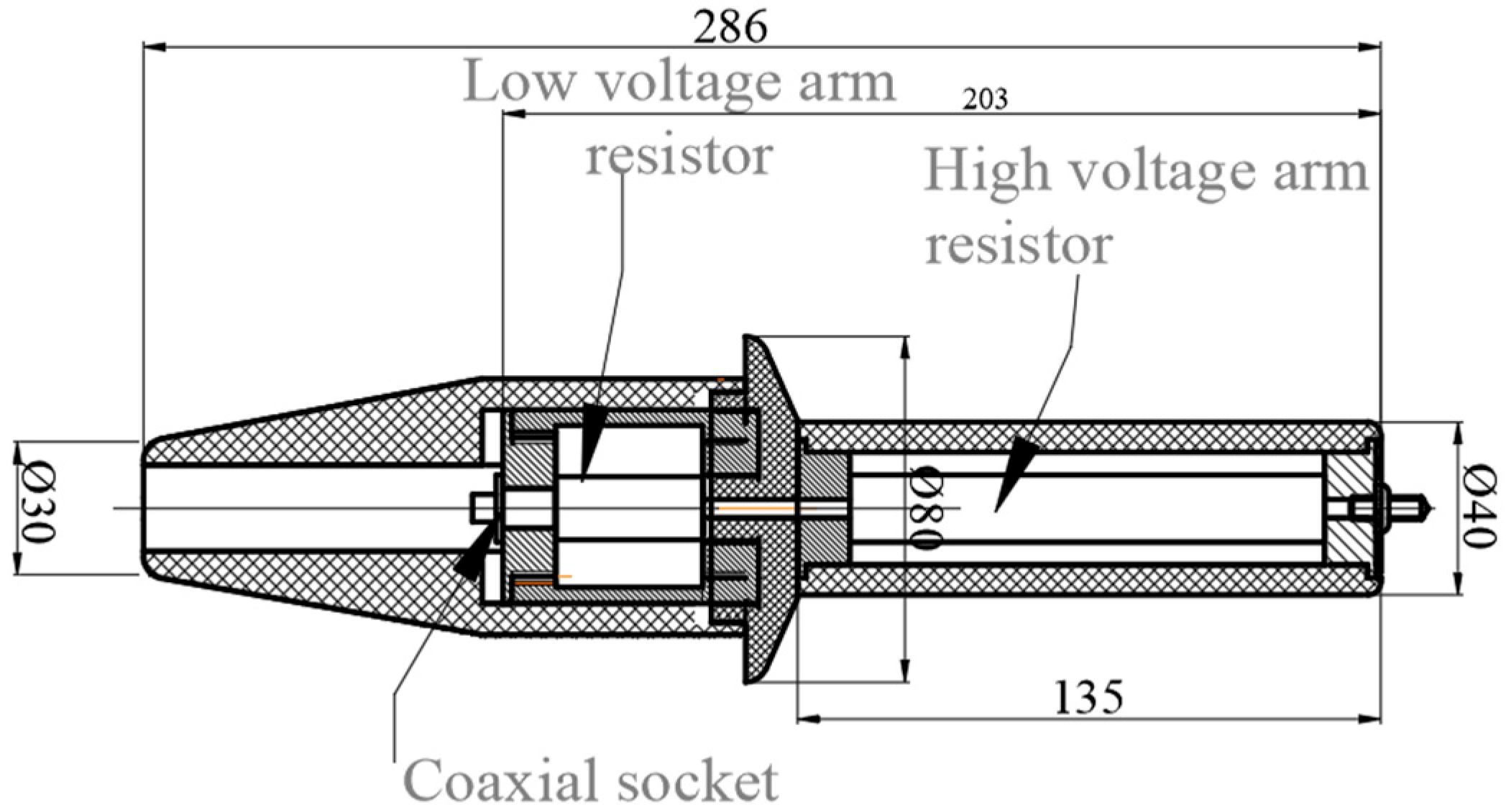
3.3.1. Structural Design

The voltage divider was designed and manufactured using metal oxide film resistors, as shown in Figure 12.
Based on the analysis of the equivalent circuit of the voltage divider, the resistance value of the nanosecond pulse resistance divider was selected in the range of 500–1000 Ω. The response time of the sensor must be in the range of 1–2 ns. Non-inductive metal oxide film resistors were chosen to ensure the stability of the scale factor of the resistive divider in the nanosecond pulse frequency domain. Furthermore, considering the skin effect in the high-frequency electromagnetic environment, the thickness of the resistive film should be less than 100 μm. The low and high voltage arms are connected in series in the coaxial structure tube core with a Teflon-insulated shell. A special metal plug was used at the high voltage end to provide a reliable connection to the generator output.

3.3.2. Response Time Measurement

The step response characteristics of the resistive divider were measured by the nanosecond square wave with a rise time of 1 ns. The voltage sensors involved in the comparison and transmission included the Tektronix P5100A, P6015A probes, and Polaris PVM-1 probes. The oscilloscope (Tektronix DPO3054) was used to record the test results, as shown in Figure 13.
It is possible to determine the square wave response time of different sensors by synthesizing the rise time, as follows:
t m e a s = t r e c 2 + t o s c 2 + t d i v i d e 2
where tmeas is the rise time of the waveform recorded by oscilloscope, tosc is the rise time of the oscilloscope (calculated according to the bandwidth of the oscilloscope), and trec is the rise time of the step square wave generator. It can be seen from the test results that the square wave response times of the developed divider, P5100A, Ps6015A, and PVM-1 probes are 1.06 ns, 0.67 ns, 1.22 ns, and 3.80 ns, respectively. Among them, the response times of P5100A and PVM-1 are generally consistent with the labeled bandwidths of 500 MHz and 80 MHz, respectively. However, the response time of P6015A is significantly different from its claimed bandwidth of 75 MHz, implying that its measurement reliability for nanosecond signals is doubtful. Meanwhile, the Polaris PVM-1 shows a large response time and is not suitable for measuring pulses with a rise time of several nanoseconds. It can be calculated that the resistance divider developed in this work has a bandwidth of approximately 300 MHz and can be used for nanosecond pulse measurement.

3.3.3. Scale Factor Verification

To deal with the lack of standard nanosecond pulse sources and standard sensors, a calibration method for the scale factor of nanosecond resistance divider based on the scale factor transfer of standard sensor was proposed. First, the resistance values of the high and low voltage arms of the voltage divider were measured under standard DC sources to obtain the static scale factor of the resistance divider, which is 1020. Subsequently, the resistance divider was measured under 1.2/50 μs lightning pulse conditions according to the calibration method specified in IEC 60060-2 [32] and compared with a standard pulse sensor with traceable scale factor to obtain the scale factor of the resistance divider under microsecond pulse voltages The results show that the average value of the equivalent scale factor of the resistance divider under 1.2/50 μs pulses is 1025, which is very closely to the static value. Lastly, to verify the reasonableness of the resistance divider used under the nanosecond pulse environment, P5100A probe with a bandwidth of up to 500 MHz was used for comparison with the developed resistance divider under 1.2/50 μs and 2.5/23 nanosecond pulses, including the measured voltage of P5100A(UP5100A), the measured voltage of resistance divider (UR), and the calibration scale factor (δ). The measured data and test waveforms are shown in Table 5 and Figure 14, respectively.
Comparing with the standard sensor, the deviation between the equivalent scale factor under 1.2/50 μs pulses and static scale factor under DC voltage is 0.49%. The scale factor of the P5100A probe was calibrated to 100.76. The average scale factor of the resistance divider measured under the nanosecond pulse environment was calculated to be 1019.01. The deviation between the scale factors under 1.2/50 μs and 2.5/23 ns pulsed is 0.21%. Based on these measurement results, it can be concluded that it is feasible to use the μs pulse standard generator and μs pulse standard divider to calibrate the nanosecond resistance divider in the absence of the nanosecond pulse calibration source and the standard sensor for nanosecond pulse measurement. However, the response time of the resistance divider must be measured to ensure that the upper limit frequency of the divider can satisfy the measurement accuracy of nanosecond voltage pulses.

4. Performance of the Nanosecond Pulse Test System

The nanosecond pulse test system consists of a pulse voltage generator and a measurement unit. The measurement unit includes the developed metal oxide film resistive divider, shielded cable, and digital oscilloscope (DPO3054). The pressure adjustment ranges of the primary pulse Marx cavity and the steepening switch cavity are 0.1~0.5 MPa and 0.1~0.8 MPa, respectively. By changing the pressure of the two independent cavities, the operating voltage of the Marx switch and the steepening switch can be adjusted to obtain stable output nanosecond pulses with a rise time of 2.3 ± 0.5 ns and a half-peak time of 23 ± 5 ns with an amplitude of 10–60 kV. Based on the performance study and calibration work of a metal oxide film resistive divider, the output capability of the nanosecond pulse test system was evaluated over a range of 60 kV. To assess the stability of the pulse test system, five voltage levels were selected, and each voltage level was measured ten times repeatedly. The relative standard deviation was utilized to describe the stability of the nanosecond voltage output. Table 6 displays the measured data, and Figure 15 presents the typical output nanosecond pulse waveforms with amplitudes (Ip) of 15 kV and 60 kV.
In the operating voltage range (15–60 kV), the maximum relative standard deviation of the peak value of the output pulse of the nanosecond pulse test system is 1.517%, the relative standard uncertainty is less than 5 ‰, which demonstrates a fairly high degree of output stability. In addition, the relative standard deviation of the nanosecond pulse test system is considered to be the synthetic relative standard deviation of the nanosecond pulse generator, the resistance divider, the measurement cable, and the oscilloscope. The maximum deviation of the DPO3054 oscilloscope is ±0.5% according to the test results of the National Metrology Calibration Center, so the maximum relative standard deviation for the nanosecond pulse generator can be deduced to be less than 1.432%.

5. Conclusions

In this paper, a nanosecond pulse generator with a five-stage Marx circuit and one-stage pulse compression was designed. A high-stability nanosecond pulse test system with a rise time of 2.3 ± 0.5 ns and a half-peak time of 25 ± 5 ns was then developed.
The component parameters were calculated by theoretical analysis and circuit simulation. The conduction performance of the output switch has a significant effect on the accuracy of the nanosecond pulse waveform and the output efficiency of the circuit. A field distortion switch based on the corona phenomenon was developed. The discharge delay of the switch is less than 10 ns and the jitter is no more than 2 ns in the operating voltage range of 65% to 85%. A metal oxide thin-film resistance divider was designed and manufactured for measuring nanosecond pulses. The measurement method of the scaling factor and response time of the divider was proposed. Furthermore, the developed nanosecond resistive divider was successfully calibrated using a μs pulse standard generator and μs pulse standard divider.
Based on the coaxial compact design, combined with the development results of the corona-stabilized switch and resistance divider, a nanosecond pulse test system was constructed, and the output performance was tested. The nanosecond pulse test system consisting of a nanosecond pulse generator and a nanosecond resistance divider can output a double-exponential nanosecond voltage pulse with an amplitude of 10–60 kV, a rise time of 2.3 ± 0.5 ns, and a half-peak time of 23 ± 5 ns. The maximum relative standard deviation of the amplitude of pulses is 1.517%, and the relative standard uncertainty is less than 5‰. The nanosecond pulse test system developed in this work has a fairly high output stability, which can be used as a calibration measurement system for nanosecond pulse generators and pulse voltage sensors. It of great theoretical significance and application value for the standardization of calibration and metrology technology of nanosecond pulses.

Author Contributions

Conceptualization and Funding acquisition, J.S.; methodology, Q.Q., H.L. and Y.W.; validation, H.L.; formal analysis, Z.J.; data curation and writing—original draft preparation, Q.Q.; resources, writing—review and editing, supervision and project administration, X.Y. All authors have read and agreed to the published version of the manuscript.

Funding

This work was supported by the State Key Laboratory of Intense Pulsed Radiation Simulation and Effect (open fund project No. SKLIPR2101).

Data Availability Statement

The data that support the findings of this study are available from the corresponding author upon reasonable request.

Conflicts of Interest

The authors declare no conflict of interest.

References

  1. Lara, M.B.; Mayes, J.R.; Mayes, M.G.; Hatfield, C.W. A modular compact Marx generator design for the Gatling Marx generator system. In Proceedings of the 15th IEEE International Pulsed Power Conference, Monterey, CA, USA, 13–15 June 2005. [Google Scholar]
  2. Carey, W.J.; Mayes, J.R. Marx generator design and performance. In Proceedings of the 25th International Power Modulator Symposium, Hollywood, CA, USA, 30 June–3 July 2002; pp. 625–628. [Google Scholar]
  3. Pecastaing, L.; Paillol, J.; Reess, T.; Gibert, A.; Domens, P. Very Fast Rise-Time Short-Pulse High-Voltage Generator. IEEE Trans. Plasma Sci. 2006, 34, 1822–1831. [Google Scholar] [CrossRef]
  4. Hahn, U.; Herrmann, M.; Leipold, F.; Schoenbach, K.H. Nanosecond, kilovolt pulse generators. Dig. Tech. Pap. 2001, 2, 1575–1578. [Google Scholar]
  5. Gilman, C.; Lam, S.K.; Naff, J.T.; Klatt, M.; Nielsen, K. Design and performance of the FEMP-2000: A fast risetime, 2 MV EMP pulser. In Proceedings of the Digest of Technical Papers. 12th IEEE International Pulsed Power Conference, Monterey, CA, USA, 27–30 June 1999; Volume 2, pp. 1437–1440. [Google Scholar]
  6. Bailey, V.; Carboni, V.; Eichenberger, C.; Naff, T.; Smith, I.; Warren, T.; Whitney, B.; Giri, D.; Belt, D.; Brown, D.; et al. A 6-MV pulser to drive horizontally polarized EMP simulators. IEEE Trans. Plasma Sci. 2010, 38, 2554–2558. [Google Scholar] [CrossRef]
  7. Gubanov, V.P.; Korovin, S.D.; Pegel, I.V.; Roitman, A.M.; Rostov, V.V.; Stepchenko, A.S. Compact 1000 ps high-voltage nanosecond pulse generator. IEEE Trans. Plasma Sci. 1997, 25, 258–265. [Google Scholar] [CrossRef]
  8. Tewari, S.V.; Umbarkar, S.B.; Agarwal, R.; Saroj, P.C.; Sharma, A.; Mittal, K.C.; Mangalvedekar, H.A. Development and Analysis of PFN Based Compact Marx Generator Using Finite Integration Technique for an Antenna Load. IEEE Trans. Plasma Sci. 2013, 41, 2684–2690. [Google Scholar] [CrossRef]
  9. Liu, Y.; Lin, F.; Hu, G.; Zhang, M. Design and performance of a resistive-divider system for measuring fast HV impulse. IEEE Trans. Instrum. Meas. 2010, 60, 996–1002. [Google Scholar] [CrossRef]
  10. Chen, J.L.; Lin, T.Y.; Bai, D.Q.; Yao, X.L. Resistive Divider with Mid-Electrode for Nanosecond High-Voltage Pulse Measurement. In Advanced Materials Research; Trans Tech Publications, Ltd.: Stafa-Zurich, Switzerland, 2013; Volume 718–720, pp. 1083–1087. [Google Scholar]
  11. Ge, Y.F.; Li, L.; Liu, Y.L.; Li, M.; Kang, Q. Design, construction, and testing of solution resistive divider applied in hundreds of kilovolts nanosecond pulse measurement. Rev. Sci. Instrum. 2014, 85, 105106. [Google Scholar]
  12. Liu, J.L.; Ye, B.; Zhan, T.W.; Feng, J.H.; Zhang, J.D.; Wang, X.X. Coaxial capacitive dividers for high-voltage pulse measurements in intense electron beam accelerator with water pulse-forming line. IEEE Trans. Instrum. Meas. 2008, 58, 161–166. [Google Scholar]
  13. He, W.; Yin, H.; Phelps, A.D.R.; Cross, A.W.; Spark, S.N. Study of a fast, high-impedance, high-voltage pulse divider. Rev. Sci. Instrum. 2001, 72, 4266–4269. [Google Scholar] [CrossRef]
  14. Rai, V.N.; Shukla, M. Simple probes and attenuators for measurement of high-voltage sub-nanosecond pulses. Meas. Sci. Technol. 1994, 5, 1396. [Google Scholar] [CrossRef]
  15. Khan, M.S.; Agazar, M.; Le Bihan, Y. Development of a Standard Measuring System for High-Voltage Nanosecond Pulse Measurements. In Proceedings of the 2020 Conference on Precision Electromagnetic Measurements (CPEM), Denver, CO, USA, 24–28 August 2020; IEEE: Piscataway, NJ, USA, 2020; pp. 1–2. [Google Scholar]
  16. Yan, J.; Mei, K.; Chen, S.; Wang, Y.; Ding, W. A Frequency Response Test Device for Nano-Second Coaxial Resistor Divider. In Proceedings of the 2019 IEEE Pulsed Power & Plasma Science (PPPS), Orlando, FL, USA, 23–29 June 2019; IEEE: Piscataway, NJ, USA, 2019; pp. 1–4. [Google Scholar]
  17. Shimotsu, R.; Wang, D.; Namihira, T. Performance of a low impedance nanosecond pulse generator. In Proceedings of the 2017 IEEE 21st International Conference on Pulsed Power (PPC), Brighton, UK, 18–22 June 2017; pp. 1–4. [Google Scholar]
  18. Wei, J.; Junna, L.; Fan, G.; Guowei, X.L.Z.; Junping, T.; Yanzhao, C.W.X. A 500 KV pulse with fast risetime for EMP simulation. In Proceedings of the IPAC2013, Shanghai, China, 12–17 May 2013; pp. 708–710. [Google Scholar]
  19. Fukuoka, H.; Iida, S.; Wang, D.; Namihira, T. Improvement of Ozone Generation Characteristics with Shorter Rise Time of Nanosecond Pulse Voltage. In Proceedings of the 2019 IEEE Pulsed Power & Plasma Science (PPPS), Orlando, FL, USA, 23–29 June 2019; pp. 1–4. [Google Scholar]
  20. Deb, P.; Sethi, B.; Rongali, L.; Meena, M.; Sharma, A. Generation of high voltage nanosecond pulses using Pulse Sharpening switch. In Proceedings of the 2021 1st International Conference on Power Electronics and Energy (ICPEE), Bhubaneswar, India, 2–3 January 2021; pp. 1–5. [Google Scholar]
  21. Huiskamp, T.; van Heesch, E.J.M.; Pemen, A.J.M. Evaluation of a 0–60 kV oil-switched picosecond rise-time 5 nanosecond pulse generator. In Proceedings of the 2013 19th IEEE Pulsed Power Conference (PPC), San Francisco, CA, USA, 16–21 June 2013; pp. 1–5. [Google Scholar]
  22. Stanković, K.; Kovačević, U. Combined measuring uncertainty of capacitive divider with concentrated capacitance on high-voltage scale. IEEE Trans. Plasma Sci. 2018, 46, 2972–2978. [Google Scholar] [CrossRef]
  23. IEC 61000-2-9; Description of HEMP Environment-Radiation Disturbance. Basic EMC Publication: Geneva, Switzerland, 1996.
  24. Chen, Z. Study on Key Technologies of Coaxial Film Capacitor for Electromagnetic Pulse Simulator. Ph.D. Thesis, Xi’an Jiaotong University, Xi’an, China, 2020. [Google Scholar]
  25. Hagelaar GJ, M.; Pitchford, L.C. Solving the Boltzmann equation to obtain electron transport coefficients and rate coefficients for fluid models. Plasma Sources Sci. Technol. 2005, 14, 722–733. [Google Scholar] [CrossRef]
  26. Liu, X.H.; He, W.; Yang, F.; Wang, H.Y.; Liao, R.J.; Xiao, H.G. Numerical simulation and experimental validation of a direct current air corona discharge under atmospheric pressure. Chin. Phys. B 2012, 21, 368–377. [Google Scholar] [CrossRef]
  27. Kovacevic, U.; Bajramovic, Z.; Jovanovic, B.; Lazarević, D.; Djekić, S. The construction of capacitive voltage divide for measuring ultrafast pulse voltage. In Proceedings of the 2015 IEEE Pulsed Power Conference (PPC), Austin, TX, USA, 31 May–4 June 2015; IEEE: Piscataway, NJ, USA, 2015; pp. 1–5. [Google Scholar]
  28. Wei, B.; Liu, H.; Liang, J.; Yuan, J.; Xie, W. A novel broadband capacitor voltage divider for measurement of ultrafast square high voltage pulse transmitted in transmission line. AIP Adv. 2020, 10, 045035. [Google Scholar] [CrossRef] [Green Version]
  29. Huiskamp, T.; Beckers, F.J.C.M.; Van Heesch, E.J.M.; Pemen, A.J.M. B-dot and D-dot sensors for (sub) nanosecond high-voltage and high-current pulse measurements. IEEE Sens. J. 2016, 16, 3792–3801. [Google Scholar] [CrossRef] [Green Version]
  30. Zhang, L.; Sun, L.; Han, Y.H.; Wang, S.; Guo, C.; Wang, C.X. Development of a Broadband Capacitive Voltage Divider for Measuring Nanosecond Impulse. In Proceedings of the 2018 2nd IEEE Conference on Energy Internet and Energy System Integration (EI2), Beijing, China, 20–22 October 2018; IEEE: Piscataway, NJ, USA, 2018; pp. 1–6. [Google Scholar]
  31. Mitra, S.; Senthil, K.; Singh, S.K.; Kumar, R.; Sharma, A. Development of a novel voltage divider for measurement of sub-nanosecond rise time high voltage pulses. Rev. Sci. Instrum. 2016, 87, 024703. [Google Scholar] [CrossRef] [PubMed]
  32. IEC 60060-2; High-Voltage Test Techniques—Part 2: Measuring Systems. Basic EMC Publication: Geneva, Switzerland, 2010.
Figure 1. Nanosecond pulse generator circuit structure.
Energies 16 04534 g001
Figure 2. Nanosecond pulse generation circuit schematic.
Energies 16 04534 g002
Figure 3. Circuit analysis of nanosecond pulse formation process. (a) Third-order equivalent circuit in primary pulse formation stage; (b) fourth-order equivalent circuit in compression stage.
Energies 16 04534 g003
Figure 4. Effect of steepening loop equivalent inductance on nanosecond pulse output.
Energies 16 04534 g004
Figure 5. Structure of the nanosecond pulse test system: (a) overall structure; (b) Marx generation circuit; (c) peaking capacitor.
Energies 16 04534 g005
Figure 6. Primary pulse and compression pulse with different action time of the steepening gap: (a) tst = 16 ns; (b) tst = 19 ns; (c) tst = 25 ns; (d) tst = 35 ns; (e) tst = 40 ns; (f) tst = 40 ns, and Marx switch recover high resistance.
Energies 16 04534 g006
Figure 7. Schematic diagram of the corona-stabilized discharge switch structure.
Energies 16 04534 g007
Figure 8. Electric field distribution in corona-stabilized discharge switch (static voltage UC = 2000 V).
Energies 16 04534 g008
Figure 9. Distribution of (a) electrons, (b) positive ions, and (c) negative ions, with an electrode curvature of 0.10 mm.
Energies 16 04534 g009
Figure 10. Maximum electron density with different radius of curvature of electrode tips.
Energies 16 04534 g010
Figure 11. Conduction delay and jitter of the corona-stabilized discharge switch under the SF6 pressures of (a) 0.1 MPa and (b) 0.2 MPa.
Energies 16 04534 g011
Figure 12. Structure of the resistance divider.
Energies 16 04534 g012
Figure 13. Square wave response of the sensor involved in the transmission: (a) developed nanosecond resistance divider; (b) P5100A probe; (c) P6015A probe, and (d) Polaris PVM-1 probe.
Energies 16 04534 g013
Figure 14. Waveforms measured by the resistance divider and P5100A probe under (a) 1.2/50 μs and (b) nanosecond pulses.
Energies 16 04534 g014
Figure 15. Waveforms of the output nanosecond pulse with (a) Ip = 15 kA and (b) Ip = 60 kA.
Energies 16 04534 g015
Table 1. Equivalent component parameters of the nanosecond pulse-generating circuit.
LoopCapacitanceInductanceResistance
Marx circuitCT = 500 pFLT ≈ 1 μHRT ≈ 2 Ω
Pulse steepening circuitCP = 200 pFLP ≈ 100 nH
Load resistorRL = 50 Ω
Table 2. Waveform parameters of the output pulse with different steepening gap action delay.
tstPrimary PulseOne-Stage Compression Pulseη
Vp */kVtr */nsVp/kVtr/nstt/ns
16 μs14.1511.5812.944.49241.891.45
19 μs16.0812.9714.483.43833.890.05
25 μs21.1216.7018.892.80919.889.44
35 μs28.1721.5921.592.30511.676.64
40 μs28.4021.8820.412.22310.371.87
* tst is steepening gap action delay; Vp is peak voltage; tr is rise time; tt is wave tail time; η is circuit output efficiency.
Table 3. Particle reaction in SF6.
Reaction TypeReaction Process
Electron collision ionizationSF6 + e→SF5 + +2e + F
Electron elastic collisionSF6 + e→SF6 + e
Electronic attachmentSF6 + e→SF6
SF6 + e→SF5 + F
SF6 + e→SF4 + 2F
SF6 + e→SF5 + F
Positive and negative ion compositeSF5 + +SF6→SF5 + SF6
SF5 + +SF5→2SF5
SF5 + +SF4→SF5 + SF4
SF5 + +F→SF6
Surface reactionF→F
SF4→SF4
SF5→SF5
SF6→SF6
SF5 + →SF5
Table 4. Comparison of nanosecond pulse sensors parameters.
PublicationsSensor TypeResponse Time/BandwidthMeasuring Range
Kovacevic et al. [27]Capacitive voltage dividerApprox. 3 ns0~100 V
Wei et al. [28]Capacitive voltage divider180 kHz–2 GHzNot provided
Huiskamp et al. [29]B-dot and D-dot sensorHundreds of ps25 kV
Liu et al. [12]Capacitive voltage divider8 ns560 kV
Rai V. N. et al. [13]Capacitive voltage divider3.5 ns130 V
Zhang et al. [30]Capacitive voltage divider4.6 ns50 kV
He W et al. [14]Resistor voltage divider1 ns150 V
7 ns60 kV
Yan et al. [16]Resistor voltage divider300 ps500 V
Liu et al. [9]CuSO4 solution resistance voltage divider13 ns170 kV
Ge et al. [11]Resistor voltage divider6.8 ns300 kV
Mitra et al. [31]CuSO4 solution resistance voltage divider1 ns15 kV
Chen et al. [10]Resistor voltage divider1.6 ns30 kV
This paper developedMetal oxide film resistance voltage divider1.06 ns80 kV
Table 5. Scale factor measurement results of the resistance divider compared with a P5100A probe.
No.UP5100A/kVUR/kVδ
μs Pulsens Pulseμs Pulsens Pulseμs Pulsens Pulse
10.4750.5740.4690.5641021.361025.46
20.9591.1500.9491.1401018.111016.44
31.4681.7501.4591.7401013.821013.39
41.9542.3301.9412.3001014.351020.74
Ave.1016.911019.01
Table 6. Amplitude parameters of the output pulses.
No.Measured Peak Value of Voltage Pulse/kV
Level 1Level 2Level 3Level 4Level 5
115.0224.7339.9052.1161.28
215.0024.8841.1352.5060.92
314.9024.6739.8051.7362.08
414.9425.3840.6552.8162.07
514.7024.6039.9252.8661.69
615.4225.3640.5051.7360.85
714.9124.4440.1350.5960.91
815.1824.6640.1150.6361.73
914.9524.6740.2951.7361.67
1015.2224.6740.8952.0061.59
Average15.0224.80640.33251.86961.479
Ds *0.20170.31640.44830.78670.4641
Drs *1.342%1.275%1.112%1.517%0.755%
Urs *4.25‰4.03‰3.51‰4.80‰2.39‰
* Ds is standard deviation; Drs is relative standard deviation; Urs is relative standard uncertainty.
Disclaimer/Publisher’s Note: The statements, opinions and data contained in all publications are solely those of the individual author(s) and contributor(s) and not of MDPI and/or the editor(s). MDPI and/or the editor(s) disclaim responsibility for any injury to people or property resulting from any ideas, methods, instructions or products referred to in the content.

