1. Introduction
The use of a low number of power switches in nonconventional power electronics power-circuit configurations is a common concept in recent proposed converter topologies. Cost, size, and weight optimization are the prime driving factors behind this technological trend. In addition, a reduction in the failure rate probability of the converter system is also a contributing factor. This power electronics topological trend paved way to a series of two-in-one converter configurations; otherwise called dual-terminal converters. These are converters that have two AC terminals that are interfaced with DC in the power-conversion process: AC–DC–AC power-converter systems. Associated voltages and currents at the two AC terminals can have the same or different frequencies. For the time being, three conceptual approaches have been deployed in configuring these converter power circuits, namely: the split-capacitor-bank approach [
1,
2,
3,
4], the parallel-common-phase-leg approach [
5], and the series-common-switch approach [
6,
7,
8,
9].
For two-level converter operation, a series of applications have been explored with these converter systems. The split-capacitor-bank-based dual-terminal converter configurations have been deployed in single- to three-phase rectifier/inverter [
1], dual-inverter [
4], and three-phase-rectifier/inverter [
2,
3] drive systems. Similarly, dual-terminal converter topologies based on the parallel-common-phase-leg approach have been utilized in single [
5] and three-phase [
6], rectifier/inverter drive systems. Extensive deployment of dual-terminal converter configurations with a series-common-switch background can be seen in these converter applications: power conditioner [
10]; energy systems for distributed generation [
11]; dual-output indirect matrix converter [
12]; back-to-back converter for DFIG [
13]; online UPS [
14], and multi-phase drive systems [
15].
In view of the general limitations of the operational performance indices of two-level inverters, multilevel inverters (MLIs) became alternative power-conditioning devices [
16].
The diode- and capacitor-clamped MLI topologies conceptually fit into single-DC-source operation. Three-level variant configurations of these single-DC-sourced MLIs are used the most to serve MLI power circuits; as the synthesis of the output voltage level increases, the inherent undue voltage fluctuations in the constituting clamping capacitor banks become a limiting factor [
17]. The three-level diode-clamped inverter, often referred to as the neutral-point-clamped (NPC) inverter, has been well researched and deployed in various industrial applications, including its derived dual-inverter system [
18]. Though all the switches in an NPC inverter have a voltage rating of half the applied DC input voltage, the high conduction losses and occupied design space of the clamping diodes are of technical concern. In [
19], a compact three-level, T-type MLI configuration was implemented with output characteristics that were on par with those of the NPC. The absence of the passive diodes in the T-type inverter topology is compromised with a full-input DC voltage rating of two of its constituting switches in a phase leg. In low- and medium-voltage high-power applications, the T-type inverter is the preferred choice, since within this voltage range, discrete IGBT switches and modules with up to 6.5 kV and 1200 A ratings exist, courtesy of the recent advancements in power-switch fabrication.
Similar to the power-conversion system in [
18], the work in [
20] presented a classical dual-output, three-level inverter system based on two independent T-type inverters that shared a common input DC source. Twenty-four active power switches were involved; of these, 50% had to withstand the overall input DC voltage stress, and were rated accordingly. In order to sustain a high tempo in the advanced search for optimized three-level, dual-terminal converter systems, commensurate power electronics power circuits with reduced component counts are imperative. Using the series-common-switch conceptual approach, the work in [
21] explored the possibility of creating two independent load systems using an active-clamped NPC. Therein, the clamping diodes were replaced with active switches, and the two upper and lower switches in a classical NPC were separated by a common IGBT switch in each of the inverter phase legs. The cathode and emitter of this common switch were the respective output node terminals, in each phase, of the two independent inverters. Depending on their modulation indices, each inverter could generate three- or five-level output line voltage waveforms, and the control approach was explicitly classic and simplified. A similar dual-output inverter topology was presented in [
22]. Therein, a mixture of diodes and shared active power switches were properly deployed to create two independent load systems. However, this series-common-switch approach inherently imposed limitations on this power circuit’s switching-states operation. This limitation was reflected in its loose grip on the neutral-point voltage control, and also impeded its capability for different frequency modes of operation.
As demonstrated in [
6], the number of inverter legs needed to configure a dual-terminal converter using the split-capacitor-bank conceptual approach was one less than that required in configuring the same dual-terminal converter using the parallel-common-phase-leg conceptual approach. However, the overall performance of this approach was superior to that of the configuration that used the split-capacitor-bank approach [
6]. Considering all the aforementioned, this paper proposes a three-level, dual-phase inverter—3-L DPI—the topological concept of which hinged on the parallel-common-phase-leg approach, and its base conceptual power circuit was derived from the three-level F-type inverter, [
23]. Two phase systems were involved in the dual-output power conversion: single- and three-phase. Both phase systems had a common three-level F-type inverter leg that resulted in a reduced component-count for the entire inverter system. A pair of three-level, one- and three-phase output voltage waveforms, of variable magnitudes and frequencies, could be generated using the proposed inverter power circuit, which had a total of 16 active power switches. The absence of one F-type inverter-leg translated to a savings of four active power switches in the 3-L DPI topology. Since the base inverter leg was the F-type, this newly configured power circuit had an inherent low cost and loss performance, as demonstrated in [
23]. The operational modulation index range for the 3-L DPI was developed that dictated the dynamic output-voltage level syntheses in both phase systems. Both inverters could simultaneously attain the maximum modulation indices of 1 and 1.1547 for one- and three-phase systems, respectively, if both inverters worked at the same frequency. For variable frequencies, either of these modulation indices could be reached by the corresponding inverters; the maximum modulation indices in the two inverters summed up to 1.5118 in this operation mode. These control attributes of the proposed 3-L DPI were enshrined in the developed boundary definitions of the operational modes of the inverter. Control of the neutral-point voltage imbalance and low-frequency oscillation of the DC-link capacitor voltages during operation were achieved by the deployment of carrier-based pulse-width modulation (CBPWM) [
23]. In the next sections, the organization of this paper is as follows: the power circuit configuration and operational principle are presented in
Section 2; the deployed CBPWM scheme is presented in
Section 3; and the simulation and experimental results are presented in
Section 4.
2. Proposed Three-Level Dual-Output Inverter Configuration
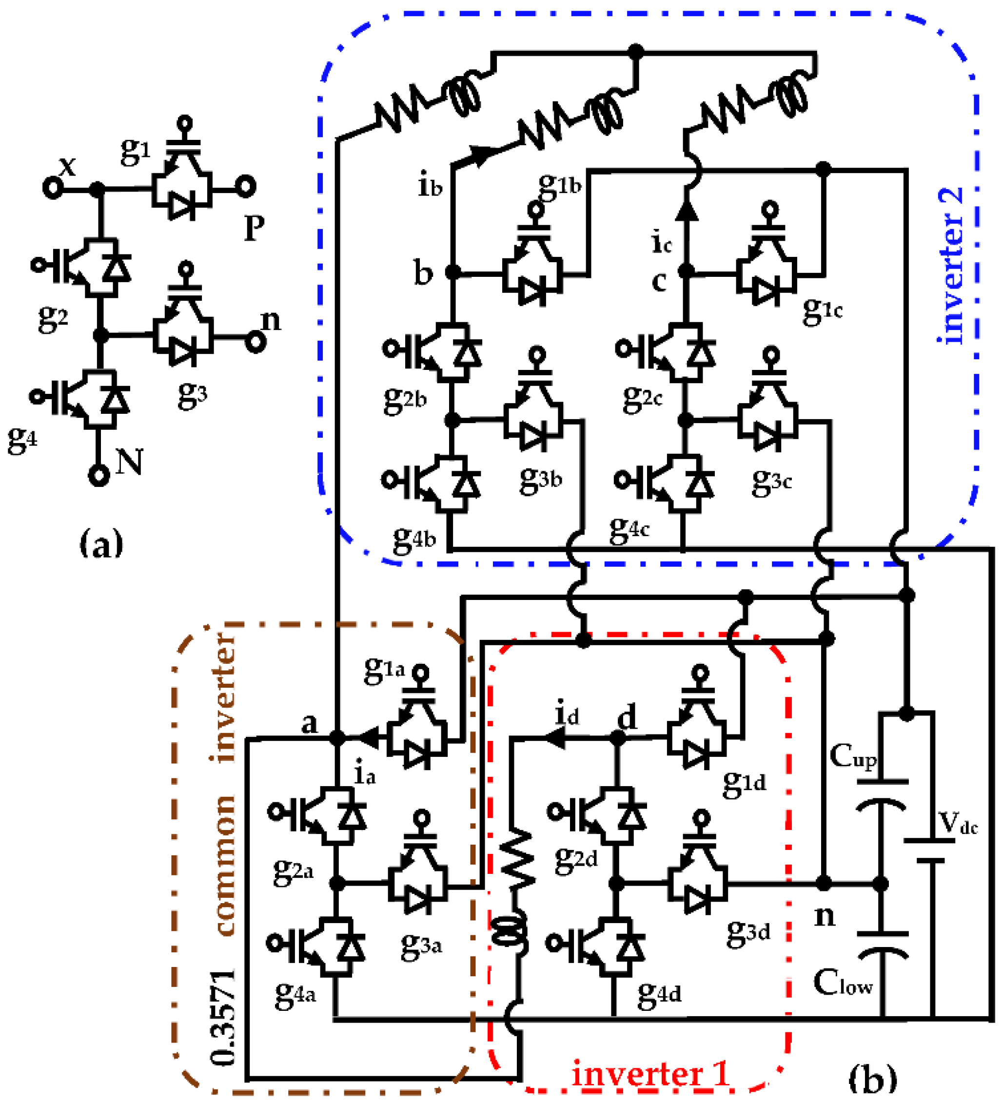
A leg of the proposed three-level dual-phase inverter is given in
Figure 1a. It had three input terminals:
P,
n, and
N, corresponding to the positive, midpoint (neutral-point), and negative-input DC (
Vdc) rails. Normally,
Vdc is split by capacitor banks with a midpoint of
n. Node
x is the output node terminal. In two-switch combinational operation, this unit leg configuration outputs three voltage values with reference to node
n.
if
g1 and g
3 are turned on;
when g
2 and g
3 are in the on-state; and
if g
2 and g
4 are switched on. These voltage level syntheses are respectively referred to as the positive, zero, and negative voltage states of the inverter unit. The switching operational principle is summarized in
Table 1. The unit inverter leg power circuit in
Figure 1a was the F-type three-level inverter leg presented in [
23]. Therein, the switching-state transitions between the voltage states of the inverter unit were explicitly demonstrated. Herein, this three-level, F-type inverter leg was utilized to configure a reduced-component-count 3-L DPI topology.
Figure 1b shows the power-circuit configuration of the proposed three-level, dual-phase inverter. Precisely, it consisted of F-type-based one- and three-phase inverters that were classically fed from common-input DC bus rails. Both were respectively configured to deliver three-level, one- and three-phase output voltage waveforms to corresponding one- and three-phase loads. The common inverter leg dually and simultaneously served both phase systems: inverters 1 and 2. This resulted in the use of 16 active power switches to synthesize these output voltage waveforms with variable amplitudes and frequencies. These output parameter indices could be the same or quite different in the two inverters. The common inverter leg was not particularized to any phase in inverter 2; only one phase could be common in both phase systems in order to eliminate four power switches. Hence, this concept also could be extended to either phase b or c in inverter 2. In addition to component-count reduction, this inverter configuration offered the additional advantage of providing an optional possibility of generating only three output line voltages in the three-phase system, or only a voltage waveform in the single-phase system, if the need arose to isolate either of the phase systems. In other words, if, as shown in
Figure 1b, inverter 1 was open/isolated from the circuit, three five-level line voltage waveforms were still generated properly by inverter 2. Similarly, if inverter 2 was open/isolated from the circuit, a single five-level voltage waveform was generated properly from inverter 1.
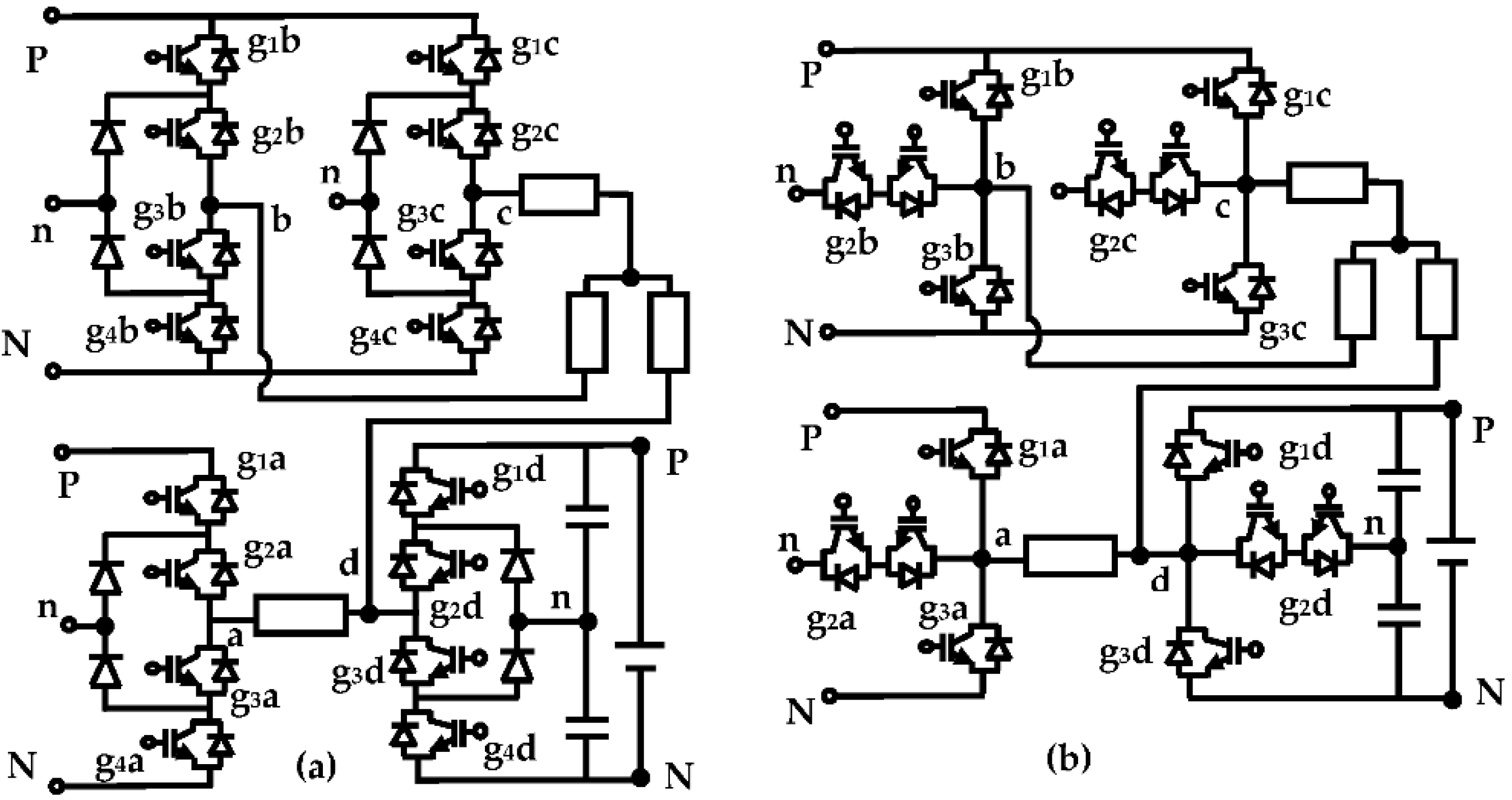
Similar dual-phase inverter configurations using the three-level diode-clamped and T-type inverter legs are shown in
Figure 2. The operational principles (switching sequences) of these inverter legs were still conserved. Functionally, the same control/modulation approach could be deployed in all the inverter configurations shown in
Figure 1 and
Figure 2. However, the topological features, including the cost and loss performances of these inverter legs, differed significantly, as explicitly demonstrated in [
23].
3. Sinusoidal PWM Strategy for the Proposed Three-Level, Dual-Phase Inverter
A lower computational burden, an individualized phase-leg operation, and ease of adaptability to multilevel/multiphase output voltage synthesis are the most cherished features of sinusoidal PWM (SPWM), and when viewed in relation to space vector PWM (SVPWM). These modulation schemes’ performance equivalence has been shown [
24], and the necessary criterion for this equality lay on the modification of the supposed sinusoidal reference signals in SPWM. Within the linear modulation region, extension of the modulation index range above unity with SPWM demanded addition of the zero-sequence component in the reference signals, following the min–max function principle [
24]. This condition equates SPWM and SVPWM in view of the utilization of the DC-link voltage. The SPWM scheme presented in [
23] fits well in the control of the proposed inverter. In addition to the min–max function modification, calculated off-set signals and voltage deviations were properly added to the modulating waveforms, which ensured stabilized and good operation of the inverter. In the proposed control scheme, inverters 1 and 2 were treated as two separate three-level, one- and three-phase F-type inverters. Since there were one and two F-type inverter legs in inverters 1 and 2, corresponding one and two reference sinusoidal waveforms, respectively, were needed to control these inverters. These references were obtained as follows.
If one- and three-phase, three-level F-type inverters were classically connected to deliver independent one- and three-phase output voltages, the needed reference signals were:
where
ω and
m are the frequency and modulation index; subscripts 1 and 2 denote inverters 1 and 2, respectively.
The maximum modulation index value for the three-phase system was (1/cos (
; that is, 1.1547, [
25]; and of course, 1 for the single-phase system. The voltage references in (1a,b) and (2a–c) were modified to fit appropriately in the control of the power circuit shown in
Figure 1b. In this proposed circuit, one inverter leg was common to both inverters. Hence, modification of the reference phase voltage signals for the one-phase system was:
For the 3-phase system, the modification was:
In the derived sets of reference waveforms,
is equal to
. With reference to the neutral point,
n, this implied that
in inverter 1 is equal to
in inverter 2. In addition, the corresponding output voltage of inverter 1,
vad, is given in (5) and the output line voltages (
vab,
vbc,
vca) in inverter 2 are given in (6a–c):
Hence, with four modulating signals
, the three-phase line voltages and a single-phase voltage were delivered at the load terminals of inverters 2 and 1, respectively, shown in
Figure 1b. The frequencies and magnitudes of these voltage waveforms in both phase systems could be the same or different in both inverters, depicting two modes of frequency operation. Thus, there was a need to establish the limits and boundary between these operational modes.
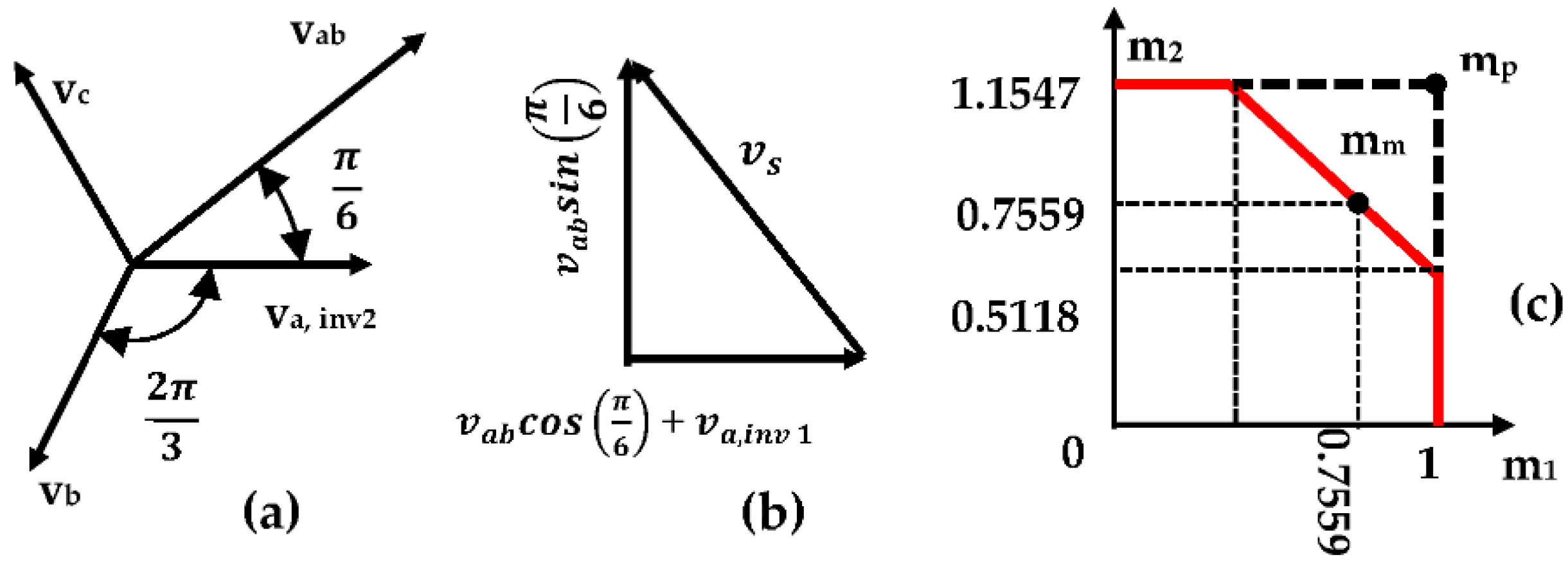
The phasor diagram of the phase voltages in the three-phase system is shown in
Figure 3a. Since the system was balanced, all the line voltages were of the same magnitude; it was sufficient to consider only
vab referenced to phase
va,inv2. As shown in
Figure 3a, the line-phase voltage relationship is given in (7):
Considering the dual-phase system, the horizontal component of
vab was in the same direction as the interfacing node
va,inv1 voltage of inverter 1. The components of the system’s voltage magnitude,
vs, are depicted in
Figure 3b; the magnitude is given in (8) in terms of the shared node voltage. Note that (3a) and (4a) are equal.
By definition, the phase system modulation index,
ms, is defined as the ratio of the phase voltage fundamental peak value, /
va,inv2/, and one-half of the DC bus voltage,
Vdc; that is:
For different frequency-mode operations in both phase systems, maximum utilization of the input DC voltage was reached when the peak value of the system’s voltage magnitude,
vs, became equal to the input DC voltage,
Vdc, a condition that set the limit of the linear modulation region. Thus:
When
is substituted in (10) from (9), the system maximum modulation index,
ms,peak, is given as:
This is the maximum modulation index for inverters 2 and 1 in this different frequency-mode operation. If
m1 and
m2 are the modulation indices for inverters 1 and 2, respectively, then:
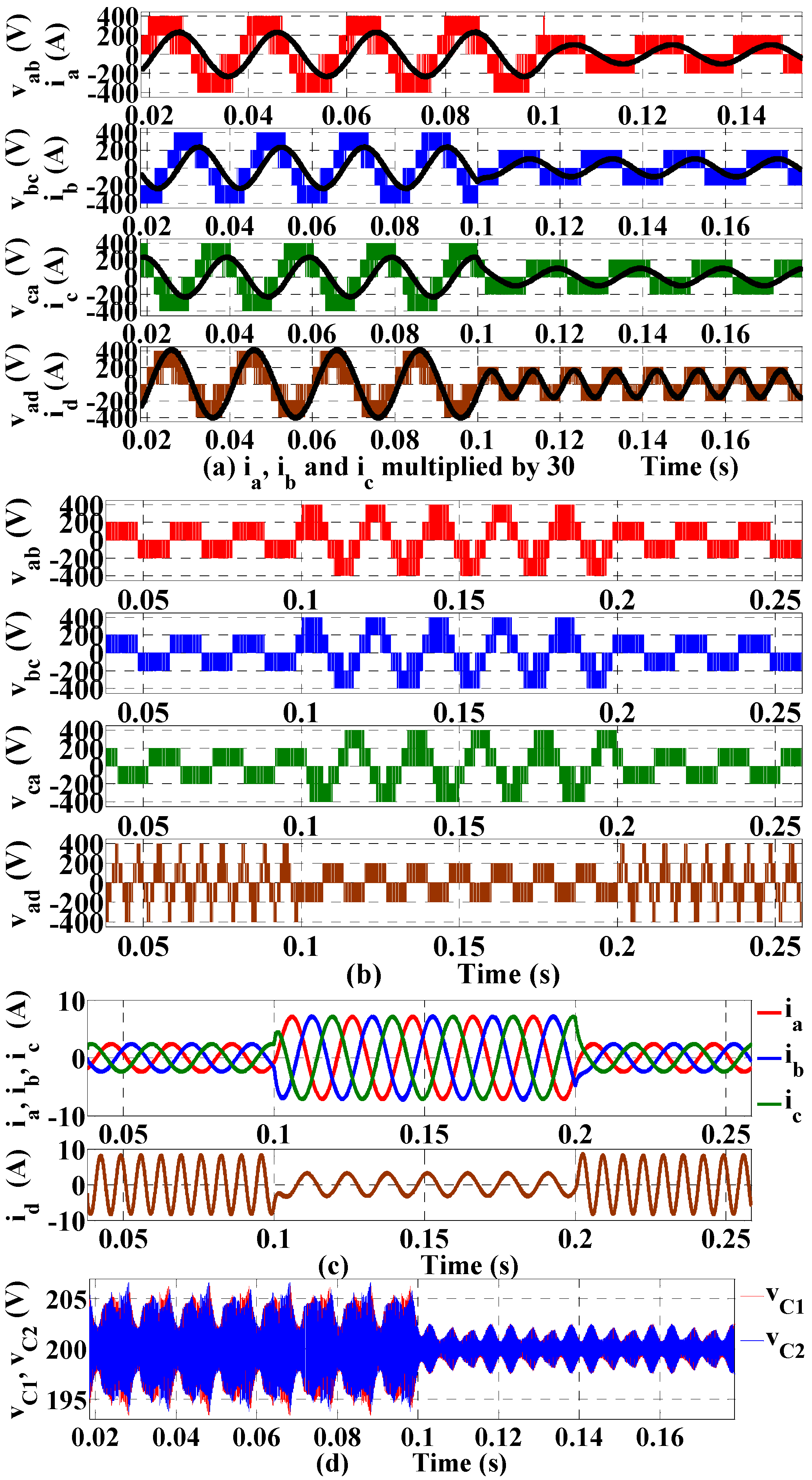
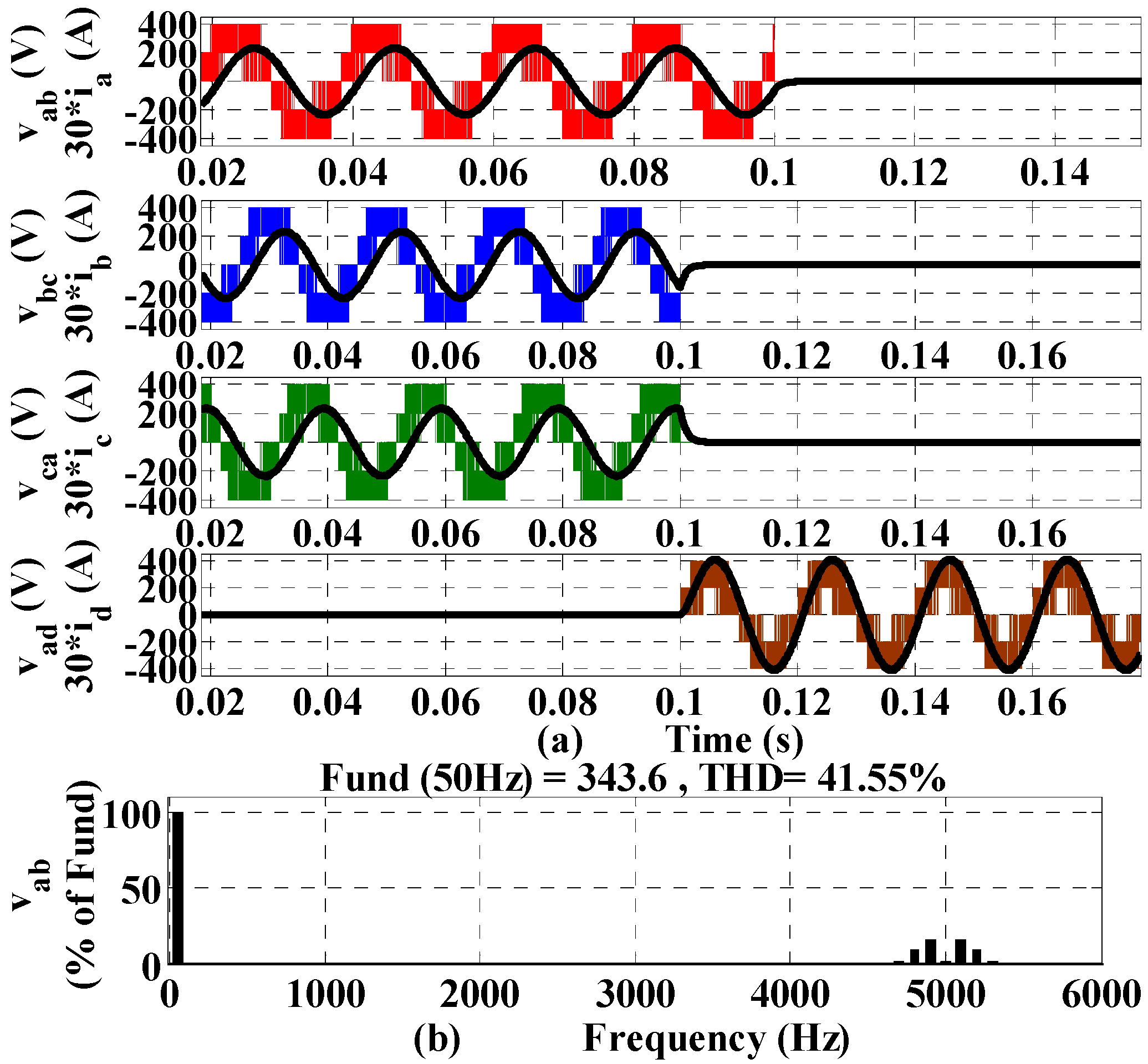
Using (12), the variation in the modulation indices in the proposed dual-phase system is shown in
Figure 3c. Therein, the area bounded by the solid-red-colored lines and the two axes defined the region where the different frequency operational mode was possible. Beyond this region, the dual-phase system had to be run in the common frequency mode operation. Depending on the combination of the modulation index values (
m1 and
m2) in this figure, three- or five-level single-phase and line-to-line three-phase voltage waveforms could be synthesized in inverters 1 and 2, respectively. Point
mm indicated the maximum equal modulation index values in both phase systems for different frequency operational modes; whereas at point
mp, the two inverters reached their respective attainable modulation index values within the linear modulation range. With
vd for inverter 1 leg,
vb and
vc for inverter 2 legs, and
va,inv2 for the common inverter leg, the modulation concept presented for the F-type inverter in [
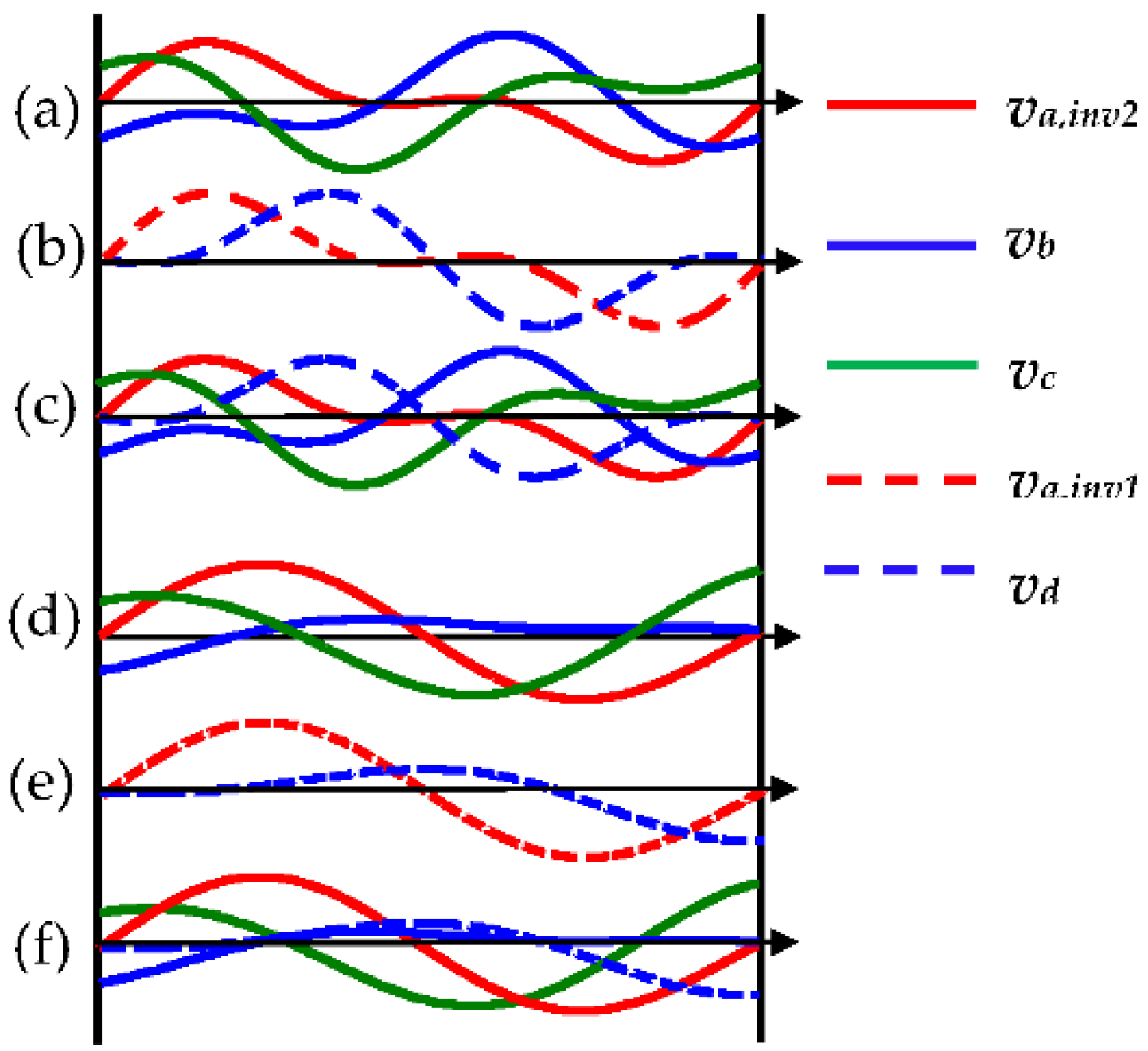
23] was used individually to generate the gating pulses for the power switches in the proposed dual-phase power circuit. The typical reference phase voltage waveforms for inverters 1 and 2 are shown in
Figure 4.
va,inv2,
vb,
vc, and
vd were the needed phase voltage references for the modulation scheme. These waveforms depict ω
2 > ω
1 operations; those for ω
1 > ω
2 operations followed suit.
Figure 4a–c corresponds to the same operational point whereby inverter 2 operated at a higher frequency than inverter 1. The obtained references, from (3a,b) and (4a–c), for inverters 1 and 2 are shown in
Figure 4a,b, respectively. The needed phase voltage reference signals for the dual-phase system are combined in
Figure 4c. Similar displays are shown in
Figure 4d–f for the two inverters operating at different modulation indices and frequencies.
It can be observed in
Figure 4a,d that the lower-frequency-operated inverter’s reference waveform periods were sectored into six equal intervals, as was obtained in [
26,
27]. Each sector spanned a 60° interval. Any sector
N (
) was defined as
Similar interval sectoring was extended to the combined waveforms shown in
Figure 4c,f. The four references, (
va,inv2,
vb,
vc, and
vd) were sequentially compared to determine these sectors, as well as their intervals. For a period of the lower-frequency-operated inverter, the four references were sampled to determine the most positive (maximum) and most negative (minimum) reference waveforms. The determined maximum (max) and minimum (min) reference signals during the sampling period clearly specified the sectors. Simple comparison and logic AND expressions in (14) and (15) could be used to determine the max and min.
With max and min computed, the sectors
Smax,min were specified and tagged with two phase notations/labels (
a,inv2,
b,
c, and
d) corresponding to the prevailing maximum and minimum phase voltage references given in
Figure 4c or
Figure 4f during the comparison period of the four reference signals. As mentioned earlier, the number of sectors,
Smax,min, precisely depended upon the frequency of the higher-frequency-operated inverter. Each of the four reference signals were compared with the max and min to determine the sectors and their intervals. A generalized expression for the sector computations is given in (16):
In the following, a recap of the modulation scheme in [
23] and its modifications to adapt to the control of the dual-phase, three-level inverter are presented.
Each inverter leg had two modulating waveforms that were used to generate the positive and negative half-cycles of the inverter-leg output voltage. These waveforms, given in (17a,b), were obtained by subtracting the max and min values in (14) and (15) from the inverter-leg reference voltage waveforms derived in (3a,b) and (4a–c). Subscript
x in (17a,b) connotes the phase notations (
a,inv2, b, c); and
pos, neg denotes the positive and negative half-cycles.
Restoration of the balance over the DC-link capacitor voltages was achieved by adding an unbalanced compensation signal,
vcomix, to (17a,b), and modifying these equations as:
where
is the respective phase current;
vC,low and
vC,up are the lower and upper splitting capacitor bank voltages in
Figure 1b; and
kcom is a proportional gain. The effects of the unbalanced compensation signal in (18a–c) were accommodated by incorporating offset signals
vcomipos in (18a) and
vcomineg to (18b), resulting in:
The currents
ipos and
ineg were determined in every sector as the currents of the particular phases for which their voltage reference signals attained their minimum and maximum values, respectively, in
Figure 4c or
Figure 4f. These currents could be determined at each of the sectors in (16) shown in
Table 2.
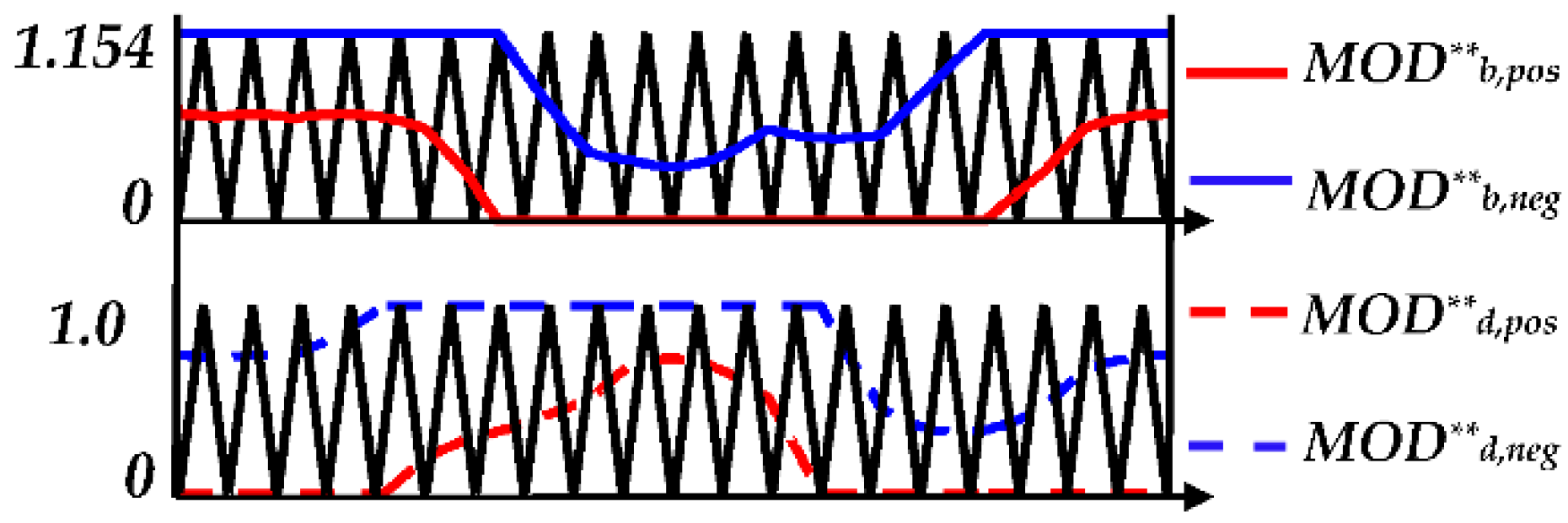
In
Figure 5, the modulation signals of inverter legs b and d were typified for
m1 >
m2 and
ω2 >
ω1; such existed for other inverter legs. The switching signals to the power switches in
Figure 1b were obtained by comparing the respective modulating waveforms with the triangular carrier signal in a simple logic operations as:
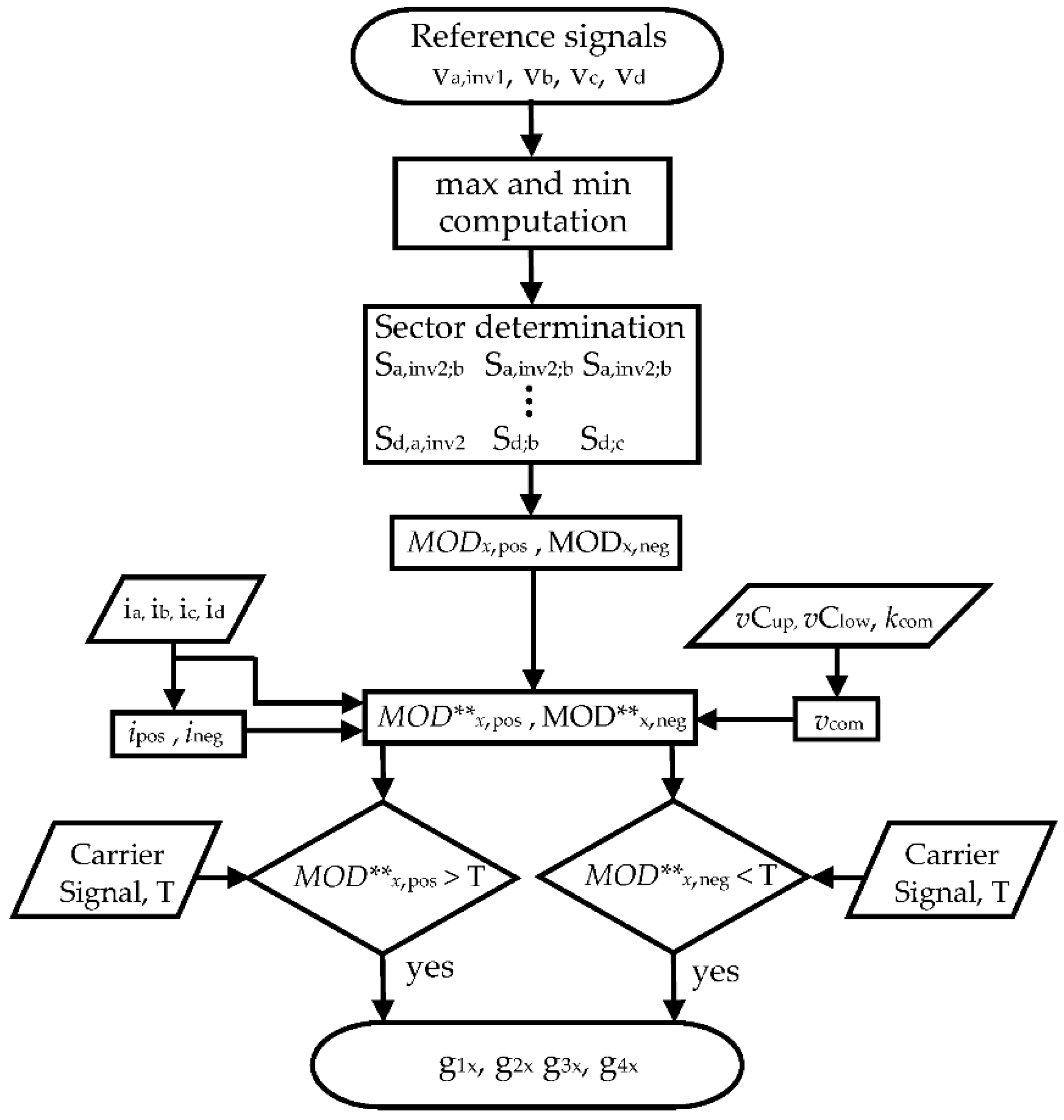
A flowchart that shows all the necessary steps for generating the gating signals of the inverter power switches is given in
Figure 6.


