Article

The Circulating Current Reduction Control Method for Asynchronous Carrier Phases of Parallel Connected Inverters

School of Electronic and Electrical Engineering, IT College, Kyungpook National University, Daegu 41566, Korea
*
Author to whom correspondence should be addressed.
Energies 2022, 15(5), 1949; https://doi.org/10.3390/en15051949
Submission received: 30 December 2021 / Revised: 1 March 2022 / Accepted: 4 March 2022 / Published: 7 March 2022
(This article belongs to the Special Issue Advances in Power Electronics Technologies)

Abstract

:
Parallel operation of inverters is one of the most effective and representative ways to increase system capacity. However, zero-sequence circulating currents occur due to the practical deviations of components constituting individual inverters in case of parallel connected inverters in which a common direct current (DC) or alternating current (AC) bus is shared. In particular, circulating currents of the high-frequency component as well as those of the low-frequency component are generated due to the asynchronization of the carriers of individual inverters. In order to suppress the circulating currents as such, the phases of the carriers should be shifted as much as the phase errors between the carriers to compensate for the phase errors. A difficulty in this phase compensation control is that when there are several pulse-width modulation (PWM) carriers, it is impossible to identify the phase of each carrier. In this paper, to overcome the problem, a method to specify the position of one of the many carriers and control the carriers and compensate for phase errors based on the relevant phase was proposed. In addition, this paper includes the analysis of circulating currents generated in the case of carrier phase errors and proposes a method to identify carrier phase errors and compensate for the relevant errors. The proposed method was verified through simulations and experiments.

1. Introduction

Currently, the penetration of renewable energy sources is increasing in the power grid due to carbon reduction and environmental protection, and the demand for DC distribution networks such as low voltage direct current (LVDC), medium-voltage direct current (MVDC) distribution, and microgrids is increasing [1,2,3,4]. Consequently, the demand for high power conversion systems is also increasing, and the parallel connection of inverters is a method mainly adopted for high power conversion. In addition, parallel connection of inverters is a method frequently used in industry because it has many advantages. The parallel inverter configuration has the advantages of enabling the securing of the scalability of system capacity and flexible operation and enabling the configuration of the system using general commercial switches [5,6]. In particular, since the magnitude of the current of each inverter connected in parallel is inversely proportional to the number of inverters connected in parallel, the system can be configured using power semiconductor switches having a relatively low rating. However, in a three-phase parallel inverter structure that shares a common DC bus and a common AC bus, there is a path through which the circulating currents can flow between the inverters connected in parallel, so that zero-sequence circulating currents (ZSCCs) appear [6,7,8,9,10]. Such ZSCCs cause problems, such as the distortion of output currents, increase in the current burden on switch devices, and electromagnetic interference (EMI).
Representative causes of circulating currents include the deviations of parameters between individual unit inverter modules, the deviation of voltage and current outputs, and carrier phase errors [7,8,9,10,11,12,13]. Among them, the carrier phase errors can occur when the PWM interleaving method is applied during parallel operation or when individual control units are used by inverter modules. When the carrier phases are in discord, a circulating current path is created due to the mismatch of the periodic switching states. Consequently, a high-frequency circulating current in the switching frequency band and a low-frequency circulating current corresponding to the third harmonics, which are the fundamental waves of the operating frequency, are generated. If the PWM interleaving method is used, total harmonic distortion (THD) of the output current of the entire system can be reduced. However, due to the intentional carrier phase errors, ZSCCs inevitably occur [14,15,16,17]. Therefore, a physical suppression method such as adding a large size filter is essential [18]. Meanwhile, if carrier phase errors occur due to the use of individual inverters, a method for reducing the ZSCCs will be required, and this condition was assumed in this paper.
Various methods for suppressing the circulating currents generated during parallel inverter operation have been previously studied. The most representative method is to physically block the path of the ZSCCs. The circulating current path between inverters can be fundamentally eliminated by using an isolation transformer on the AC side of the parallel inverter [19]. However, since this method requires a low-frequency transformer, there is a disadvantage that the volume of the system becomes large. A similar method is to isolate the DC links of individual inverters independently [20,21]. In this method, since the DC voltage must be controlled by each inverter, as many voltage sensors as the number of parallel inverters are required, such that the system becomes complicated. On the other hand, there is a method of disposing passive elements having a high impedance, such as coupled inductors in the circulating current path [14,22]. In this method, as the number of inverters connected in parallel increases, the system becomes more complex and the volume also increases. The method of using the LCL filters for the outputs of individual inverters can be hardly used universally because the optimal design must vary according to the field of application. Although the circulating currents can be suppressed by controlling the circulating currents with software using active control such as proportional and integral (PI) and proportional and resonant (PR) control, it is not suitable for controlling the high frequency circulating currents in the switching frequency band due to the limitation of the control bandwidth [18,19,20,21,22,23,24,25,26]. Therefore, in order to reduce the circulating currents due to the carrier phase errors, a new appropriate control method is necessary. Although there have been previous studies that proposed control methods for carrier phase error, they have a limitation in that they targeted two parallel inverters [7,12,13].
In this paper, a circulating current reduction control method applicable to an inverter in which two or more inverter modules are connected in parallel is proposed. The composition of this paper is as follows. In Section 2, circulating currents are defined and the characteristics of circulating currents in N parallel inverters due to carrier phase error are analyzed. In Section 3, a method that can suppress and control circulating currents by judging the occurrence of carrier phase error and setting an inverter that has the reference carrier among N carriers is proposed. In Section 4, the results of simulation for the verification of the proposed method are shown. In Section 5, the proposed method is verified using the experimental results. In Section 6, the last chapter, the conclusion is described.

2. Basic Definition for Circulating Current Reduction and Control and Analysis of the Principle of Occurrence

2.1. Definition of Circulating Currents in Parallel Inverters

Before analyzing the circulating currents, the relationship between the output current and the circulating current in parallel inverters is defined. The structure of N parallel inverters is as shown in Figure 1, where individual inverters are connected to a common AC bus and share a common DC link voltage. The total output current of one phase of parallel inverters is defined as the sum of the output currents of individual inverters, as shown in Equation (1). In Equation (1), x represents one of a, b, and c phases, i x . j refers to the output currents of individual inverters, n refers to the number of inverters connected in parallel, and j refers to the order of individual inverters.
i x = j = 1 n i x . j
In an ideal case, the output currents i x . k for one phase of k-th inverter module share the average of the total output current. However, due to the circulating currents, the circulating currents i x . k . c i r passing through the corresponding phase are included and the output currents are expressed as shown in Equation (2).
i x . k = i x n + i x . k . c i r
The circulating currents i x . k . c i r passing through one phase of individual inverters shown in Equation (2) are defined as interphase circulating currents (ICC). By substituting Equation (1) into Equation (2), the ICC can be expressed as shown in Equation (3).
i x . k . c i r = n i x . k j = 1 n i x . j n = j = 1 n i x . k i x . j n = j = 1 ( j k ) n i x . k i x . j n
When all the ICC of individual inverters shown in Equation (3) are added up, the sum is expressed as shown in Equation (4) and becomes 0.
j = 1 n i x . j . c i r = ( i x . 1 i x . 2 ) + ( i x . 1 i x . 3 ) + + ( i x . 2 i x . 1 ) + ( i x . 2 i x . 3 ) + + ( i x . n i x . ( n 1 ) ) n = 0
As for Equation (4), the sum of the three phases also becomes 0.
x = a , b , c ( j = 1 n i x . j . c i r c ) = x = a , b , c ( k = 1 n ( j = 1 ( j k ) n i x . k i x . j n ) ) = 0
The ZSCC i 0 . k of individual inverters are defined as Equation (6).
i 0 . k = i a . k + i b . k + i c . k 3
When the output currents of all inverter modules are entire system is balanced, the sum of the three-phase output currents of all inverters appears as 0 as shown in Equation (7), and in this case, the sum can be expressed as the sum of the ZSCCs of individual inverters.
i a + i b + i c = ( i a . 1 + i b . 1 + i c . 1 ) + ( i a . 2 + i b . 2 + i c . 2 ) + + ( i a . n + i b . n + i c . n ) = 3 j = 1 n i 0 . j = 0
The ZSCC in one inverter in Equation (7) can be expressed as shown in Equation (8).
i 0 . k = j = 1 ( j k ) n i 0 . j = { ( i a 0.1 + i a . 2 + + i a . ( k 1 ) + i a . ( k + 1 ) + + i a . n ) + ( i b . 1 + i b . 2 + + i b . ( k 1 ) + i b . ( k + 1 ) + + i b . n ) + ( i c . 1 + i c . 2 + + i c . ( k 1 ) + i c . ( k + 1 ) + + i c . n ) } 3 = j = 1 ( j k ) n i a . j + j = 1 ( j k ) n i b . j + j = 1 ( j k ) n i c . j 3
If ( n 1 ) i 0 . k is added to both sides of Equation (8), Equation (9) will be established.
n i 0 . k = ( n 1 ) i a . k + i b . k + i c . k 3 { ( i a .1 + i a .2 + + i a . n ) + ( i b .1 + i b .2 + + i b . n ) + ( i c .1 + i c .2 + + i c . n ) } 3 = ( n 1 ) i a . k + i b . k + i c . k 3 j = 1 ( j k ) n i a . j + j = 1 ( j k ) n i b . j + j = 1 ( j k ) n i c . j 3 = j = 1 n ( i a . k i a . j ) + j = 1 n ( i b . k i b . j ) + j = 1 n ( i c . k i c . j ) 3 = j = 1 ( j k ) n ( i a . k i a . j ) + j = 1 ( j k ) n ( i b . k i b . j ) + j = 1 ( j k ) n ( i c . k i c . j ) 3
If Equation (9) is organized with referenced to Equation (3), the sum of the ICC of each phase will appear so that Equation (10) will be established.
i 0 . k = x = a , b , c i x . k . c i r 3 n
That is, the ZSCCs in the three-phase parallel inverters can be expressed as the sum of the ICC. Using the definition of circulating currents, the occurrence of circulating currents in the case of carrier phases errors can be analyzed.

2.2. High-Frequency Circulating Current Due to PWM Phase Errors during Parallel Operation

During parallel inverter operation, the periodic switching state mismatch between inverters occurs due to the presence of carrier phase errors. Due to the mismatch of the switching states, a closed circuit including DC links between the individual inverters is formed. Since the switching state mismatch appears twice in one cycle of the carrier, the frequency band of the circulating currents is the same as the PWM carrier frequency band. Figure 2 shows the principle of generation of circulating currents in the case of carrier phase errors due to the operation of single-phase two-parallel half-bridge circuits. In the operation shown in Figure 2, the two inverters operate with carriers with different phases and output voltages based on the same voltage reference. Due to the different carrier phases, a time Δ t in which the switching states of individual inverters are inconsistent occurs and circulating currents can flow through the closed circuit during this time. In cases where the voltage reference is a discrete signal, the width of Δ t always has a constant value. A circulating current i 12 . c i r between inverters is generated through the closed circuit constructed at this time.
Figure 3 shows the equivalent circuit of the closed circuit constructed in the case of a switching state mismatch due to a carrier phase error. The equivalent circuit is composed of the inductance of each inverter and a voltage source in which the voltages in the form of pulses of V D C , 0, V D C are periodically appearing. In this case, the pulse width of each voltage is the time of mismatch ( Δ t ) of the switching state, and the circulating current ( Δ i 12 . c i r ) generated during this section can be expressed with Equation (11). In Equation (11), Δ t becomes to be proportional to the degree of the error of the carrier phase. Based on the definition in Equation (3), the circulating current between the two inverters can be expressed as the difference between the amounts of changes Δ i 1 , Δ i 2 in the output current of individual inverters during Δ t . The direction of the circulating current between the two inverters varies depending on the switching state. When S 1 = 1 , S 2 = 0 , a voltage of V D C is applied to the impedance in the circulating current path, and when S 1 = 0 , S 2 = 1 , a voltage of V D C is applied. The voltage V D C applied in this circulating current path appears alternately during one cycle of the carrier of V D C .
Δ i 12 . c i r c = Δ i 1 Δ i 2 2 = V D C L s h 1 + L s h 2 Δ t ( S 1 = 1 , S 2 = 0 ) V D C L s h 1 + L s h 2 Δ t ( S 1 = 0 , S 2 = 1 )
Therefore, in Equation (11), the two switch states also appear alternately during one cycle. The magnitude of the circulating current of the switching frequency component generated at this time can be expressed with Equation (12).
i 12 | f s w = | V D C L s h 1 + L s h 2 Δ t |
The analysis of circulating currents in two parallel inverters can be expanded to the analysis of circulating currents in N parallel inverters. In the case of N parallel inverters, since N carriers can exist, the relationships between the leading and lagging of the phases of individual carriers are changed so that circulating currents appear complexly, the analysis of the entire circulating currents is complicated. However, the relationship between the circulating currents generated in the two inverters among the N parallel inverters is similar to the relationship between the circulating currents generated in two parallel inverters. Therefore, the principle of circulating current generation in two parallel inverters can be applied to analyze the circulating currents of N parallel inverters. The individual terms of the phase circulating currents in Equation (3) can express the circulating current relationship between the corresponding inverter and another inverter. If there is a carrier phase error between the k-th inverter and the j-th inverter among N parallel inverters, an equivalent circuit as shown in Figure 3 will be formed between the two inverters. Each term in Equation (3) can be expressed with as circulating current generated between two inverters among N parallel-connected inverters using Equation (11). Therefore, the circulating current generated from the k-th inverter to the j-th inverter can be defined with Equation (13).
Δ i k j . c i r c = Δ i k Δ i j n = V D C L s h k + L s h j Δ t k j ( S k = 1 , S j = 0 ) V D C L s h k + L s h j Δ t k j ( S k = 0 , S j = 1 )
The voltage pulse width at this time is the switching mismatch time Δ t k j between the two inverters. The magnitude of the equivalent voltage generated by the voltage pulse as such varies depending on the switching state of each inverter. That is, the order of operation of the switch in the half-cycle section in which the carrier rises according to the phase relationship between the carriers is different from that in the half-cycle section in which the carrier falls. Consequently, the sign of changes in the circulating current flowing from the k-th inverter to the j-th inverter when the phase ( θ k ) of the k-th carrier leads the phase ( θ j ) of the j-th carrier is opposite to that when the phase ( θ k ) of the k-th carrier lags behind the phase ( θ j ) of the j-th carrier. That is, the sign of the change amount during the switching mismatch time is determined by the leading and lagging relationship between the phases of individual carriers. Therefore, the circulating currents in the switching frequency band can be defined as shown in Equation (14) in consideration of the sign of the change amount in the circulating currents.
i k j . c i r c | f s w = | V D C L s h k + L s h j | Δ t k j ( θ k < θ j ) | V D C L s h k + L s h j | Δ t k j ( θ k > θ j )
The sign according to the phase in Equation (14) means the direction of the circulating current flowing from the k-th inverter to the j-th inverter depending on to the relative positions between carriers. When using Equations (3), (13) and (14) to represent the phase circulating currents of individual inverters in the switching frequency band, the phase circulating currents can be expressed with Equation (15).
i x . k . c i r c | f s w = i x . k 1 . c i r c | f s w + i x . k 2 . c i r c | f s w + i x . k n . c i r c | f s w
The terms on the right side of Equation (15) become to have different signs depending on the phase relationship between the carrier of the relevant inverter and the carrier of another inverter. If the carrier of the k-th inverter is leading in the forefront, θ k < θ j will be satisfied for all terms, so that all the circulating currents have the same direction. In cases where the phase of the carrier lags the most, the direction of all the circulating currents is the same as θ k > θ j is satisfied. When both carriers with a leading phase and carriers with a lagging phase exist based on the carrier of the k-th inverter, all the signs of individual terms in (15) are not the same, so that the magnitude of (15) is reduced by the offsetting components between the circulating currents. That is, it can be seen mathematically that the circulating current in the switching frequency band of the inverter having the most leading carrier phase or the most lagging carrier phase has the largest value.

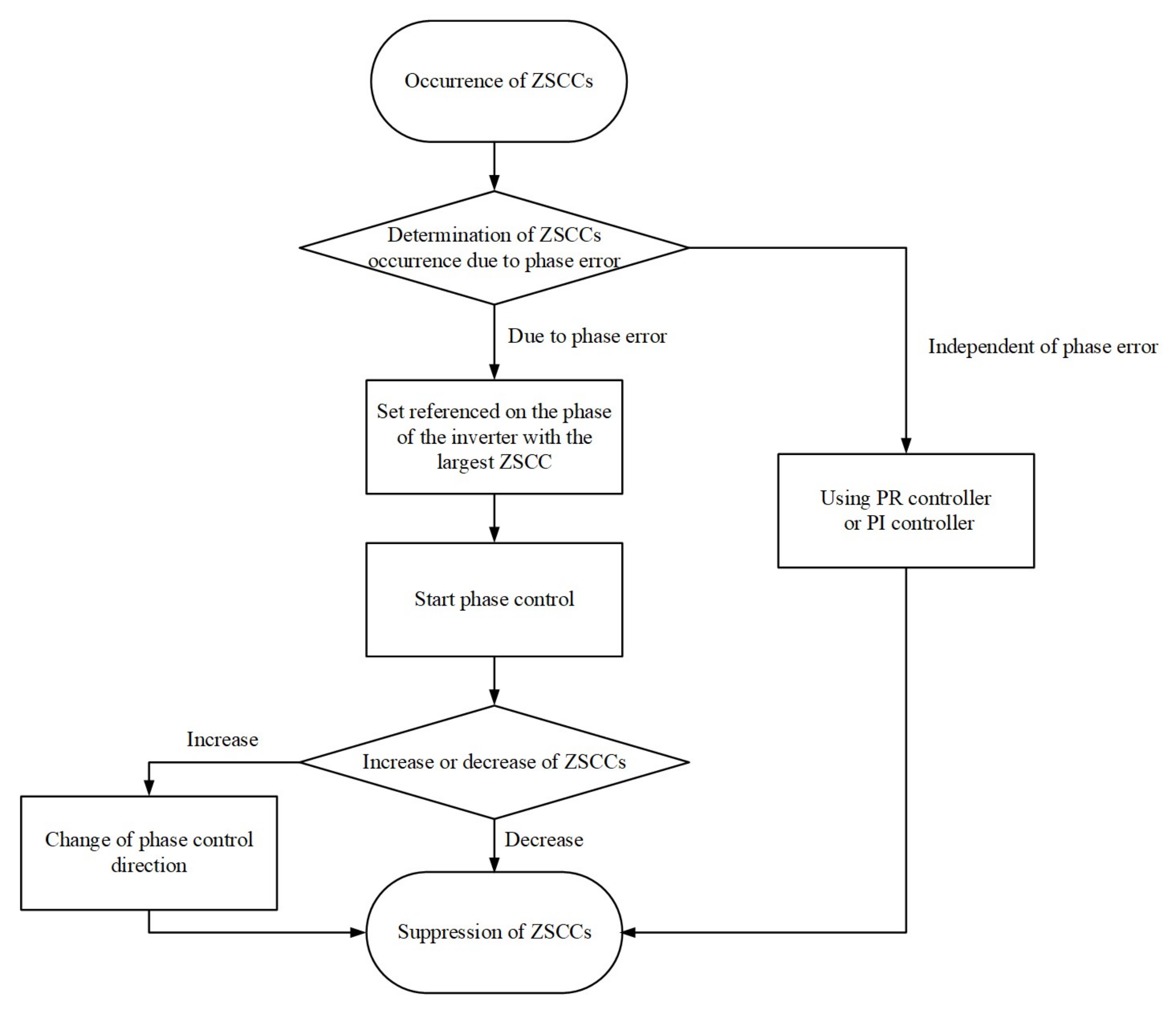
3. Proposed Carrier Phase Compensation Method

In this chapter, a control method to reduce circulating currents when phase errors occur between carriers in cases where there are N carriers is proposed. Section 3.1 deals with the detailed operation of the overall control configuration due to carrier phase errors. Section 3.2 discusses methods to provide stable control against various disturbances that can cause carrier phase errors, such as additional inverter input.

3.1. Operation Principle of Carrier Phase Control Method

Figure 4 shows the proposed control method, which is divided into three parts. First, the output current of each inverter is measured to calculate ZSCCs, and then the ZSCC that is the control reference is selected. Second, whether or not to proceed with control and the direction of compensation for the phase errors between carriers are determined. Finally, the phases of the carriers are controlled. The detailed operation principle for each part is as follows.

3.1.1. Calculation of Zero-Sequence Circulating Currents of Inverters and Setting of Control Criterion

The output currents of individual inverter modules are sampled, and ZSCCs are calculated thereafter. When the control unit of the inverter samples the currents at a frequency corresponding to twice the carrier frequency, the difference between the previous sampling value and the current sampling value becomes the magnitude of the currents in the carrier frequency band. However, since negative and positive numbers appear alternately in the calculation as such, absolute values are taken in order to use constant values for control.
Since the proposed method carries out the control of multiple carriers, an appropriate carrier should be set as a reference carrier. The carrier phase of the inverter that outputs the circulating current of the largest value then develops to have the most led or the most lagged phase. Therefore, if the largest circulating current is set as the reference current ( i 0 . r e f | f s w ) for control, the control can be executed based on the carrier having the most leading phase or the most lagging phase. However, the inverter module that generates the largest circulating current may be changed during control due to reasons such as disturbances during parallel inverter operation, and the inverter module which has the largest circulating current becomes to output the reference current.

3.1.2. Carrier Phase Error Determination and Control Direction Setting

The magnitude of a ZSCC is proportional to the phase error of the carrier. Therefore, the occurrence of a carrier phase error can be indirectly estimated using the magnitude of the reference ZSCC. When the magnitude of a ZSCC is equal to or greater than the control start criterion (CSC), a value compensating for the carrier phase error is output using an integrator. The ZSCC value corresponding to the CSC should be designed considering the error or offset in the current measurement so that there is no effect of the relevant values on control.
The proposed method designates a reference carrier through the method described in Section 3.1.1. and thereafter compensates all carrier phases in one direction. In this case, since it is impossible to specify whether the phase of the reference carrier is the leading or lagging behind the phases of all other carriers, a method of setting the direction of compensation control is necessary. To determine the direction of phase compensation of the controller, a direction alteration criterion (DAC) that can change the direction of the phase compensation in cases where the magnitude of the circulating current increases by more than a certain value after the ZSCC control is started is set. If the magnitude of the ZSCC does not decrease after control started, it can be determined that the direction of compensation for phase errors is incorrect. The DAC is set by selecting the maximum allowable current value when the direction of compensation is wrong. However, when a sudden phase error occurs, such as when a new inverter is inserted, the DAC may be exceeded regardless of whether control has been started or not. In this case, since the validity of the direction of compensation must be re-evaluated, a method to assist it is required. This will be dealt with in detail in Section 3.2.

3.1.3. PWM Carrier Phase Compensation Control

When the factors of whether or not to control carrier phase errors and the direction of phase compensation have been set, the control of carrier phases begins. The carrier phase of the inverter having the reference zero-sequence current becomes the reference, and the carrier phases of other inverters are made to match with the reference carrier. However, the phases of other carriers cannot be known based on the phase of the reference carrier, and the phases of all carriers are controlled at the same speed. Therefore, a method to relatively adjust the control of carriers is required, and in this paper, the magnitude of the circulating current between inverters is used. The ZSCC between two inverters due to the carrier phase error can be expressed as shown in (16) by (5) and (10).
i 0 . k i 0 . j n = ( i a . k i a . j ) + ( i b . k i b . j ) + ( i c . k i c . j ) 3 n
According to Equation (13), the smaller the carrier phase error between the two inverters, the smaller the result of Equation (16). Due to the characteristic as such, the smaller the phase difference from the reference carrier is, the smaller becomes the difference between the reference ZSCC and the circulating current of the corresponding inverter relatively as the control progresses. Therefore, if the result of (16) becomes smaller than the CSC, the method of stopping the carrier phase control of the corresponding inverter is used. In case where this method is used, compensation is completed first from the carrier located close to the reference carrier so that relative control according to the carrier phase is possible.

3.2. Control Method When Carrier Phase Disturbance Has Occurred

Situations such as the initial start-up of parallel inverters and the input of an additional inverter during operation act as an abrupt disturbance in the carrier phase in the parallel inverters. When an abrupt disturbance or the like occurs in the carrier phase, an abrupt time difference of Δ t occurs in the inter-carrier phase. When this time difference occurs, a circulating current proportional to the time difference generated by Equation (11) or (13) is generated. The magnitude of this time difference has a different value depending on the degree of inconsistency when a disturbance occurs. When a circulating current is generated due to a time difference, carrier phase control for suppressing the circulating current is performed, and the time difference is decreased or increased according to the control direction of the phase. In order for the proposed control method to operate normally in a situation where disturbance occurs, a method to identify the appropriateness of the direction of compensation of the control is additionally required. This section introduces a method to check the trend of ZSCCs to identify the appropriateness of the direction of phase error compensation when disturbance occurs.
To identify the trend of ZSCCs, the past value of the reference ZSCC value that is being output by the controller is defined. Immediately after the occurrence of disturbance, the magnitude of circulating currents increases rapidly, and as the control progresses, the circulating current shows a decreasing or increasing trend. In cases where the current value is decreasing when the past value of ZSCCs is output, a crossing point occurs, and this is defined as decreasing crossing. In cases where the current value increases, no crossing with the past value occurs. Whether or not such a crossing has occurred can be identified by the sign of the difference between the two values, because the difference between the present value and the past value of the zero-sequence current changes from a positive value to a negative value at the decreasing crossing. The adequacy determination as such can be applied to two cases; (1) when a disturbance occurred in the phase during normal operation, and (2) when a disturbance occurred while controlling the phase error.

3.2.1. Control Method When Phase Disturbance Occurred during Normal Operation of Parallel Inverters

Figure 5 shows the conceptual trend of the present and past values of the reference ZSCC and the difference between the present value and the past value intended to identify whether a crossing point between the two values has occurred or not in cases where an abrupt phase disturbance has occurred in a situation of normal operation without any carrier phase error. The upper section in each figure shows the present and past values of the reference ZSCC. The present value is indicated by a red line, and the past value is indicated by a blue line. The past value represents the same value as the present value, but has the same value at a later time than the present value on the time axis. The middle section indicates the difference between the present value and the past value. When a sudden disturbance has occurred in the phase between carriers, the controller immediately begins to operate. In this case, if the direction of compensation for the phase error is the direction to reduce the error, the ZSCC decreases as shown in Figure 5a. As the present value of the ZSCC decreases, a decreasing crossing with the past value occurs, and the difference between the two values changes from a positive to negative value. If the direction of compensation for the phase error is the direction to increase the error, the ZSCC increases as shown in Figure 5b. When the ZSCC increases, no decreasing crossing occurs and the difference between the past value and the present value maintains a positive sign. Therefore, when the decreasing crossing occurs, it can be seen that the direction of compensation for the phase error is valid, and when the decreasing crossing does not occur, it can be seen that the current direction of compensation is wrong, and that the direction should be changed.
The concept termed direction alteration detection signal (DADS) is used to determine the validity of the direction of phase compensation. This is shown in the bottom section of Figure 5, and the red line represents the present value and the blue line represents the past value, which is different from the present value and past value of ZSCC. This signal is set to be activated when the reference ZSCC exceeds the phase compensation direction alteration criterion and to be reset by decreasing crossing. The past value of the signal is defined and used to determine the validity of the control. The value of the signal at a point before the point at which the past value of the ZSCC is memorized is selected as the point at which the past value begins to be memorized. In the case of Figure 5a, the DADS is activated by a sudden increase in circulating currents after a phase disturbance occurred. As the control progresses, the ZSCCs decrease, and the signals are deactivated by the decreasing crossing. In case where a decrease crossing has occurred, the present value is not activated when the past value of the DADS is active, so that it can be seen that the direction of control is appropriate. Therefore, the phase compensation direction is not changed by force and the control can achieve the purpose of reducing the circulating currents. In the case of Figure 5b, the compensation direction is not appropriate after the disturbance occurred. As the control progresses, the ZSCCs increase, and no decreasing crossing occurs. Therefore, the DADS remains active. If no decreasing crossing occurs, the present value will be maintained when the past value of the compensation DADS is activated. Cases where both signals are active means that the compensation direction is inadequate. When the compensation direction is inappropriate, a compensation direction forced change signal (DFCS) is generated to reverse the compensation direction for the phase error. As the compensation direction for the circulating current is reversed, the ZSCCs show a decreasing trend and the carrier phase is normally compensated.

3.2.2. Control Method When an Additional Disturbance Occurs during Parallel Inverter Phase Compensation Control

The proposed method inevitably requires time from the start to the completion of the control of the phase error. If any disturbance such as inverter dropout or temporary malfunction occurs during this time, the ZSCCs may increase again and the appropriateness of the compensation direction must be re-evaluated. Figure 6 shows the conceptual trends of the present value and the past value of the ZSCC when a disturbance occurred during phase control and the difference between the present value and the past value in order to check whether a crossing point between the two values has occurred or not. The upper section in each figure shows the present and past values of the reference ZSCC. The present value is indicated by a red line, and the past value is indicated by a blue line. The past value represents the same value as the present value, but has the same value at a later time than the present value on the time axis. The middle section indicates the difference between the present value and the past value. The ZSCCs increase again thereafter due to a disturbance suddenly occurring while a decreasing trend was shown (while being normally well controlled), and a point at which the present value and the past value of the ZSCC cross occurs. This crossing point is defined as an increasing crossing. When an increasing crossing has occurred, the sign of the difference between the present value and the past value changes from negative to positive one, and the appropriateness of the control direction must be determined again. Further, the control criterion may be changed due to a change in the inter-carrier phase relationship. Figure 6a shows a case where the compensation direction is appropriate after the increasing crossing, and the decreasing crossing occurs again. Figure 6b shows a case where the compensation direction is not appropriate after increasing crossing, and ZSCCs increase without any occurrence of decreasing crossing.
Figure 6 also shows the determination of the adequacy of the direction of compensation for the phase error after an increasing crossing and whether the compensation direction should be changed or not. To determine the adequacy of the compensation direction, an increasing crossing detection signal (ICDS), which is activated when an increasing crossing occurs, is used. This is shown in the bottom section of Figure 6, and the red line represents the present value and the blue line represents the past value, which is different from the present value and past value of ZSCC. This signal is deactivated by a decreasing crossing. As with the DADS, the past value of the ICDS is collected at a point earlier than the past value of the zero-sequence current. In Figure 6a, the ZSCC decreases after the occurrence of the increasing crossing, and the present value of the ICDS is deactivated due to the decreasing crossing. Cases where the present value the ICDS is deactivated when the past value of the ICDS is activated mean that the control direction is appropriate. Therefore, the direction of control is maintained and the trend of ZSCC decreases as control progresses. In Figure 6b, the ZSCC increases after the occurrence of an increasing crossing, and no decreasing crossing occurs. The present value of the ICDS remains active. Cases where when the past value of the ICDS is activated, the present value is activated means that no decreasing crossing has occurred, indicating that the direction of the phase control is not appropriate. Therefore, the direction of compensation for phase errors is reversed when it is identified that both signals are active. As the direction of compensation for the circulating current is reversed, the ZSCC shows a decreasing trend and the carrier phase is normally compensated.
The overall flow of control is shown in Figure 7. In case that the generation of ZSCCs is due to the carrier phase error, the carrier phase is directly controlled by applying the control method mentioned in this paper. When the generation of ZSCCs is not due to the carrier phase error, the control method introduced in [13] is applied to suppress the ZSCCs.

4. Simulation Results

Through simulations, the phase errors were simulated for two cases; a case where disturbance occurred in the carrier phase during normal operation and a case where disturbance occurred in the carrier phase during phase control. The simulations proceeded to simulate the three parallel inverter structure in the inverter structure in Figure 8. The load condition was set as a simple resistor-inductor R-L (resistor-inductor) load. The parameters of the simulations are as shown in Table 1. The simulation was implemented with Matlab Simulink PLECS (Plexim GmbH, Zurich, Switzerland). The controller was configured using Simulink and the plant was configured using PLECS.

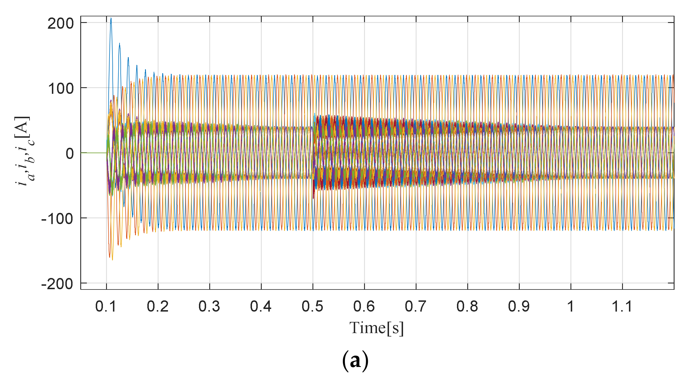
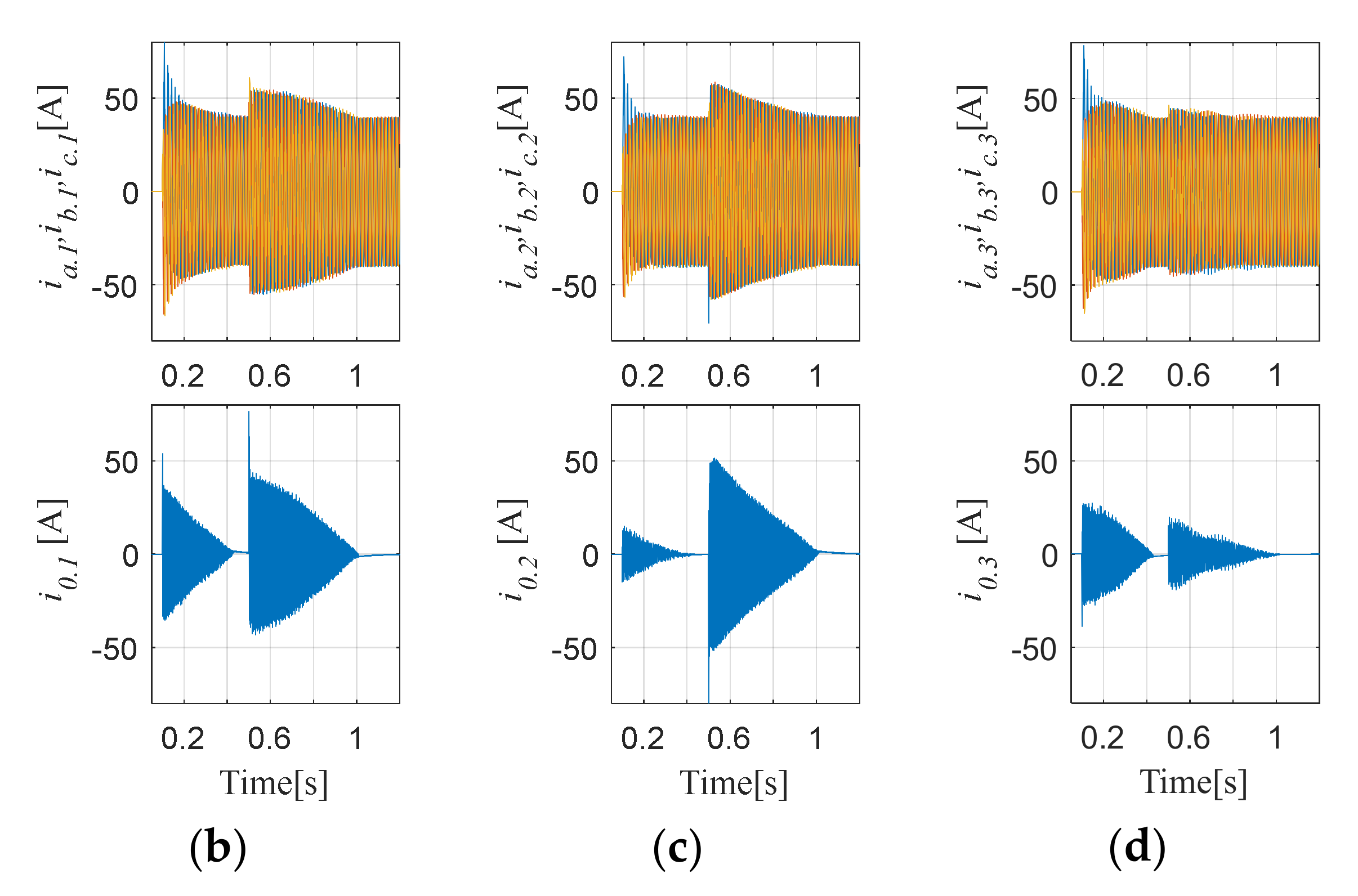
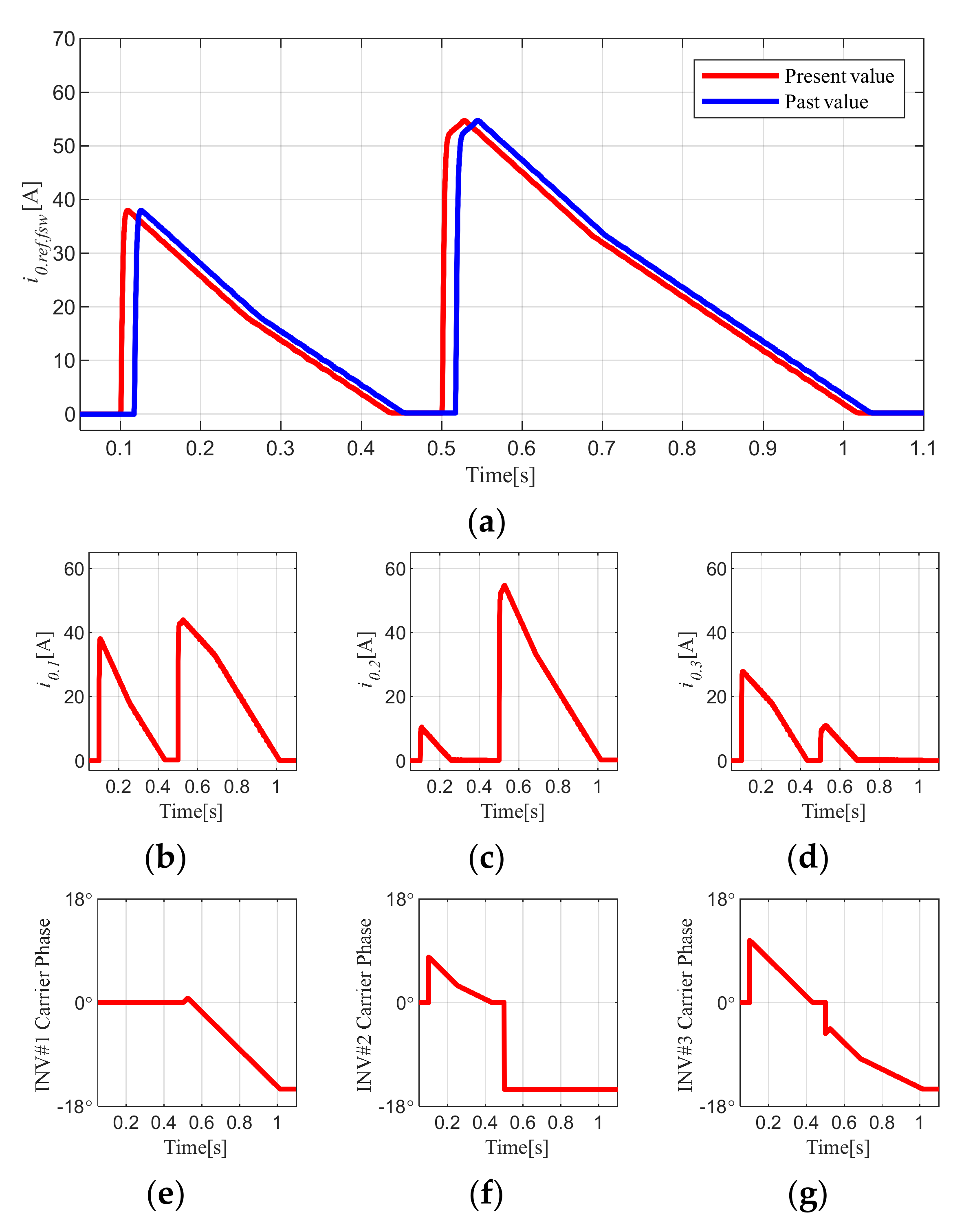
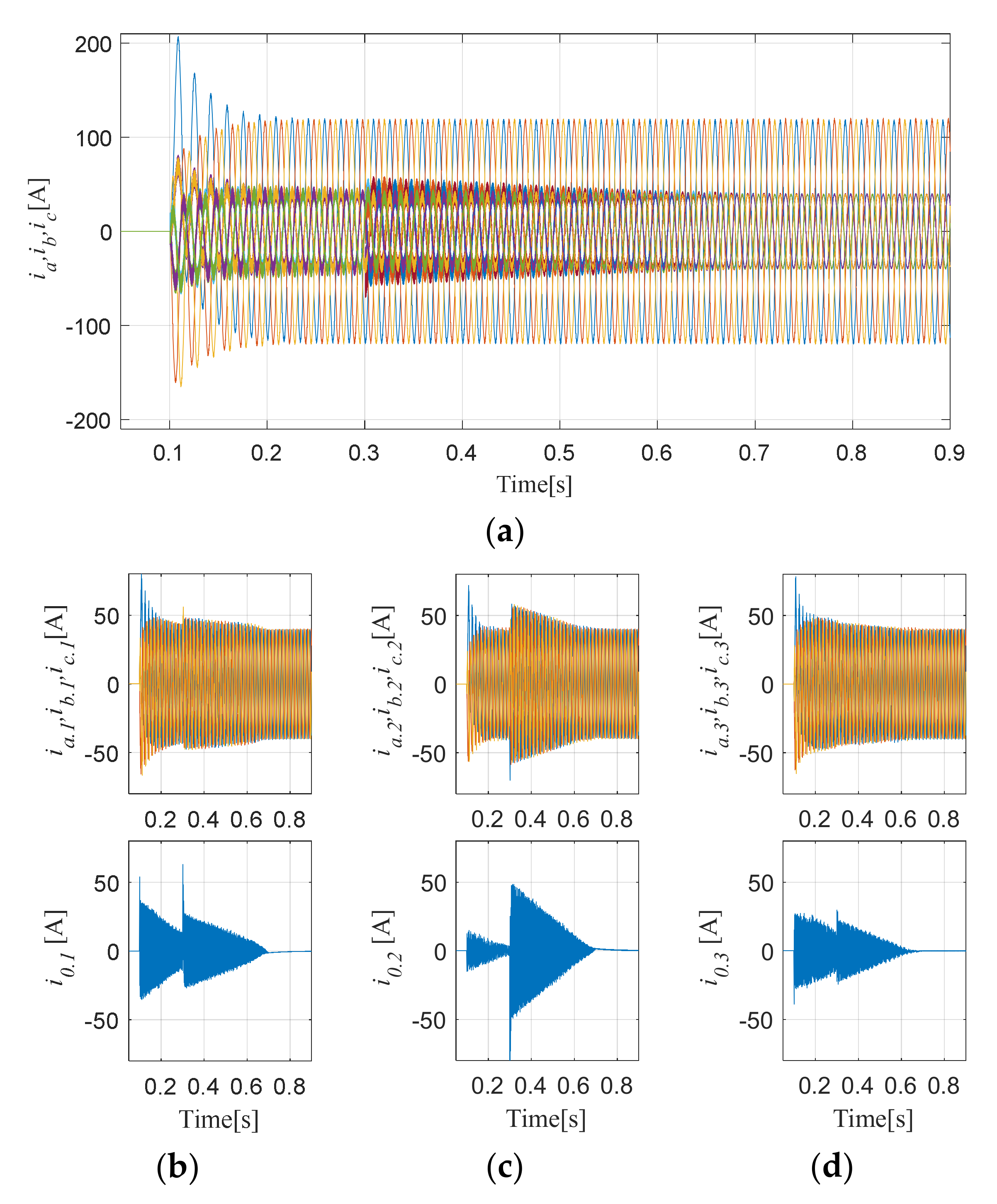
4.1. Results of Simulation of Phase Disturbance Occurring during Normal Operation

In order to verify the control operation, a phase error of +7.92 degrees in inverter 2 and a phase error of +10.8 degrees in inverter 3 were generated based on inverter 1 at 0.1 s in the simulation. Thereafter, a disturbance of −7.2 degrees to inverter 2 and a disturbance of +5.4 degrees to inverter 3 were additionally generated at a time of 0.5 s in the simulation.
Figure 9 shows the total output current, the output current and ZSCC of each inverter as a result of the simulation. It can be seen from the simulation results that the output current of each inverter was sharply distorted when a disturbance occurred at 0.1 s. In addition, it can be seen that the ZSCC also increased rapidly. As the control progressed, the distortion of the output current was eliminated and the magnitude of the ZSCC also decreased. When an additional disturbance occurred at 0.5 s, the output current was sharply distorted once again. However, it can be seen that as the control progressed, the distortion of the output current was reduced, and the zero current was also reduced. After the control for each disturbance was completed, the distortion in the output current of each inverter was eliminated and the ZSCC was reduced to within the allowable range.
Figure 10 shows the trend of the ZSCC set as the control criterion, the trends of ZSCCs of individual inverters, and the carrier phases of individual inverters. As shown in Figure 10a, when the disturbance occurred at 0.1 s, the reference ZSCC rapidly increased to about 40 A. Thereafter, the control proceeds and a decreasing crossing occurs.
The zero-sequence current decreases and the control is completed at about 0.43 s. When a disturbance occurred at 0.5 s, the reference ZSCC increased to about 55 A. As the control progressed, the circulating current showed an increasing trend for about 0.03 s, and no decreasing crossing occurred. Therefore, the compensation direction was forcibly changed by the control operation. After the change of the compensation direction, a decreasing crossing occurred, and the control was completed at about 1.03 s. The control operation completion time is affected by the gain value of the integrator in Figure 4. Figure 10b–d shows the trend of ZSCCs of each inverter. The circulating current of inverter 1 has the largest value for the disturbance at 0.1 s, and the circulating current of inverter 2 has the largest value for the disturbance at 0.5 s. Therefore, for the disturbance at 0.1 s, the carrier phase of inverter No. 1 is used as a reference for control and for the disturbance at 0.5 s, the carrier phase of inverter No. 2 is used as a reference for control.
Figure 10e–g shows the carrier phases of individual inverters. When controlling for disturbance of 0.1 s, the carrier phase control was performed in the direction consistent with the phase of the carrier of the inverter 1. When the control was completed, the phases of inverters 2 and 3 were shifted by about −7.92 degrees and −10.8 degrees, respectively. When a disturbance occurred at 0.5 s, the new phase error was added to the previously compensated phases of −7.92 degrees and −10.8 degrees, so that inverter 2 had a phase of about −15.12 degrees and inverter 3 had a phase of about −5.4 degrees. In this case, the ZSCC of inverter 2 outputs the largest value. Therefore, the phase control proceeded in the direction coincident with the carrier phase of inverter 2. Finally, when the control was completed in the simulation, the phase of each inverter coincided with the phase of inverter 2.

4.2. Results of Simulation of Phase Disturbance Occurring during Phase Control Operation

To verify the control operation, a disturbance of +7.92 degrees in inverter 2 and a disturbance of +10.8 degrees in inverter 3 were generated based on inverter 1 at 0.1 s in the simulation. Thereafter, in the simulation in which phase control is in progress, a disturbance of −7.2 degrees in inverter 2 and a disturbance of +5.4 degrees in inverter 3 were additionally generated at a time of 0.3 s.
Figure 11 shows the total output current of all inverters, the output currents of individual inverters, and the ZSCC in the simulation results. Control began when a disturbance occurred at 0.1 s, and the ZSCC began to decrease. It can be seen that when an additional disturbance occurred at 0.3 s, the ZSCCs of individual inverters sharply increased and the distortion of the output currents intensified. It can be also seen that when the control of the additionally occurred disturbance was in progress, the distortion of the output currents was reduced, and the ZSCCs were also reduced. Finally, the distortion of the output currents is reduced and the ZSCC is also reduced to within the set range.
Figure 12 shows the trend of the ZSCC set as the control criterion, the trends of the ZSCCs of individual inverters, and the carrier phases of individual inverters. As shown in Figure 12a, control began when a disturbance occurred at 0.1 s. When an additional disturbance occurred at 0.3 s, the reference ZSCC increased to about 90 A, and an increasing crossing occurred. As the control proceeded after the occurrence of the increasing intersection, the ZSCC decreased, and a decreasing crossing occurred so that the control direction was maintained. Control for the phase error was completed at about 0.7 s. Figure 12b–d shows the trends of the ZSCCs of individual inverters. It can be seen that the ZSCCs rapidly increased in all inverters when the additional disturbance occurred at 0.3 s. While the control was in progress following the first disturbance based on the ZSCC of inverter 1, another disturbance occurred at 0.3 s, and the control was performed based on the ZSCC of inverter 2. Therefore, as shown in the result in Figure 12e–g, it can be seen that following the first disturbance at 0.1 s, the carrier phases of inverters 2 and 3 were controlled based on inverter 1 but when the additional disturbance occurred, the carrier phases of inverters 1 and 3 were controlled based on inverter 2.

5. Experiment Results

The proposed method was verified through experimentation. For the experiment, a 10 kVA-rated parallel active front end (AFE)-inverter contraction experiment set as shown in Figure 13 was constructed. The simple RL load power supply conditions of the inverter were set as experimental conditions. The parameters used in the experiment are the same as those in the simulation in Table 1. However, the load condition was set to 6 kVA in consideration of the rating of the experimental set. In addition, during the experiment, the disturbance condition was applied at 1/10 the level of the simulation.

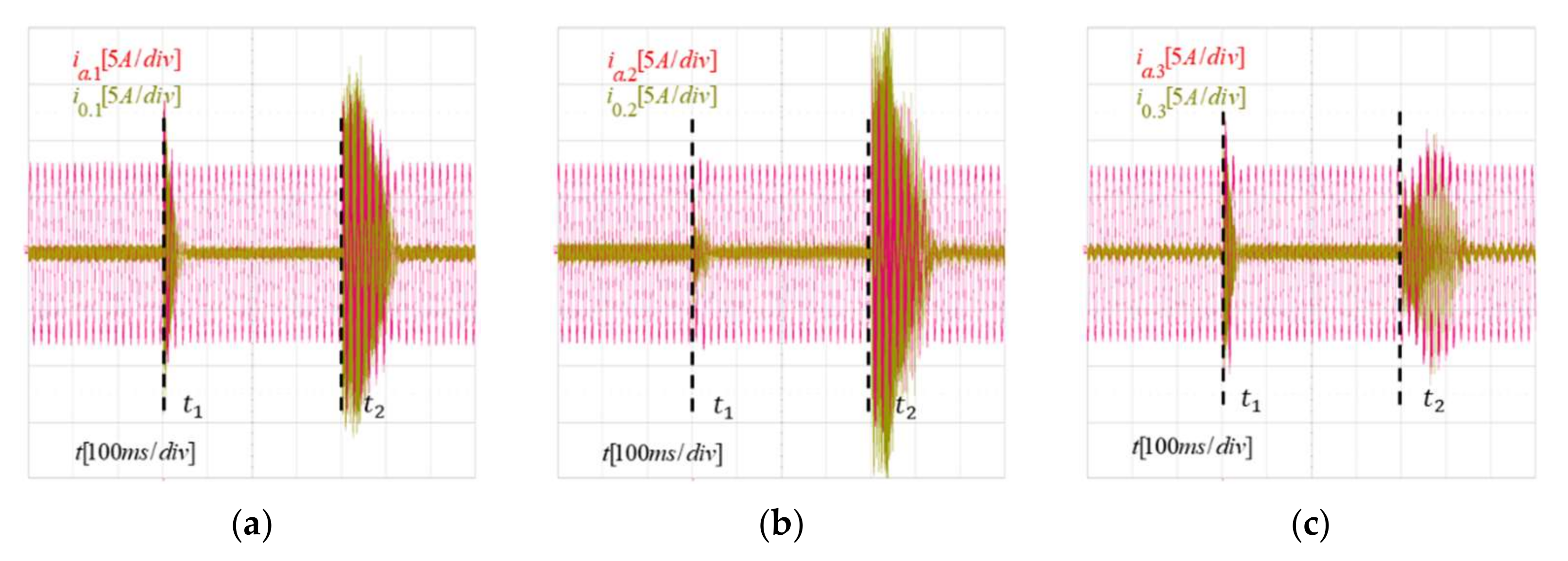
5.1. Results of Experiments for Phase Disturbance during Normal Operation

In order to verify the control operation when a phase disturbance occurs during normal operation, a total of two disturbances were generated during operation under similar conditions to the simulation in Section 4.1. Figure 14 shows the experimental results. This experimental result corresponds to Figure 9e–g, which is the simulation result of Section 4. Disturbances were simulated at times t 1 and t 2 shown in Figure 14, respectively. It can be seen that when each disturbance occurred, the ZSCC increased, and the output current was distorted. Following the disturbance at time t 1 , the ZSCC increased to a maximum of 8 A, and following the disturbance at time t 2 , the ZSCC increased to be about 20 A. With the application of the proposed control method, the phase error due to disturbance was compensated, the distortion of the output current was eliminated, and the ZSCC was also reduced. In addition, when comparing Figure 9e–g, which is the simulation result, and Figure 14, which is the experimental result, it can be seen that the occurrence and decrease of the ZSCCs at the point of occurrence of each disturbance are similar. However, since the experimental conditions are reduced, the magnitude and reduction time of the ZSCC are very small compared to the simulation.
In Figure 15, the yellow, red, and blue lines represent the phase angles ( θ 1 , θ 2 , θ 3 ) of the inverter, respectively, and the green line represents the reference ZSCC i 0 . r e f | s w . This experimental result corresponds to Figure 10a,e–g, which is the simulation result of Section 4. The reference zero-sequence current was applied with a low-pass filter in consideration of the noise generated during inverter operation. The experimental result in Figure 15 shows that when the disturbance at time t 1 was applied, the phase compensation direction was appropriate, such that the ZSCC began to decrease immediately after the disturbance, indicating that the control proceeded without any forced change in the compensation direction. However, it can be seen that when the disturbance at t 2 was applied, the ZSCC temporarily showed an increasing trend, and the phases of individual carriers were compensated in a direction that does not coincide with the phase of inverter 2, which is the reference inverter, so that the phase compensation direction was changed by forcing and the ZSCC was reduced so that the phases of individual inverters were controlled in a direction to match the phase of inverter 2. It can be confirmed that similar results were obtained when comparing Figure 10a,e–g, which are simulation results. As in the simulation, control was performed without changing the control direction for the first disturbance, and the control direction was changed for the second disturbance.
The validity of the proposed control method can be verified with the experimental results in this section. The proposed method can be used in situations where synchronization between inverters is not maintained during operation, for example, when additional inverter input is required in parallel-connected inverters.

5.2. Results of Experiments for Phase Disturbance Occurring during Phase Control Operation

In order to verify the control operation when phase disturbance occurs during phase control operation, disturbances were generated under similar conditions to the simulation in Section 4.2. Figure 16 shows the experimental results. This experimental result corresponds to Figure 11e–g, which is the simulation result of Section 4. When a disturbance occurred at time t 1 shown in Figure 16, the ZSCCs showed a decreasing trend due to phase control. However, it can be seen that when an additional disturbance occurred at time t 2 , the ZSCC increased up to about 15A at the maximum, and the distortion of the output current intensified. As the control progressed, the magnitude of the ZSCCs began to decrease again generally, and the sharp distortion of the output currents was removed. When comparing the experimental results of Figure 16 with Figure 11e–g, it can be seen that ZSCC shows a similar trend. It can be seen from the two results that there was a rapid increase in ZSCC at the point of occurrence of each disturbance and a decrease by control. This is because the experiment was conducted under similar conditions to the simulation, and it can be confirmed that the control operated according to the design intent.
The experimental results in Figure 17 show the reference zero-sequence current and the carrier phases of individual inverters when an additional disturbance occurred at t 2 while the disturbance at t 1 was being controlled. This experimental result corresponds to Figure 12a, e–g, which is the simulation result of Section 4. The increase in circulating currents when the disturbance occurred at t 2 can be identified through the reference ZSCC in Figure 17. Due to the increase in the circulating current, an increasing crossing is identified inside the controller. However, the compensation direction is not changed by force since the control direction maintains appropriateness. It can be seen that when the disturbance occurred at t 2 while the existing disturbance at t 1 was being controlled based on the carrier phase of inverter 1, the disturbance was controlled based on the carrier phase of inverter 2. As the control progressed after the increasing crossing, the reference ZSCC showed a decreasing trend, and the control was completed over time. The experimental results in Figure 17 are similar to the simulation results in Figure 12a,e–g. When the first disturbance and the second disturbance occur, the trend of the carrier phase is similar, and the reference ZSCC also shows a similar trend.
The method proposed in this section was also verified through experiments. The proposed method can be applied when additional disturbance occurs during control of the phase error, such as, for example, when one inverter is tripped off.
As a result, it was confirmed through an experiment that the generation of circulating current can be suppressed. When circulating current occurs, switching loss, conduction loss, and heat loss increase due to unnecessary converter inner current increases by the circulating current. These losses can be reduced by suppressing circulating current.

6. Conclusions

In this paper, a method to control the circulating currents caused by carrier phase errors when N parallel inverters are operated was proposed. When parallel inverters are used, circulating currents become a cause of declines of the efficiency of the inverters. In particular, the carrier phase errors between inverters resulting from the use of individual control units make it impossible to apply the general control strategy. Therefore, a new control method must be applied including an effective control method for sudden disturbance that may occur during parallel inverter operation. The control unit can identify the occurrence of disturbance and can carry out control without specifying the accurate position of the reference carrier phase by determining the validity of the compensation direction. In addition, the proposed method has the advantage that it can be used universally regardless of the number of parallel inverters connected. To determine the validity of the control, a 32 kVA-rated three parallel inverter simulation was performed. As a result of the simulation, it was identified that abrupt phase changes can be controlled, and ZSCCs can be reduced. Actual 6 kVA-rated three parallel inverters were experimented and a significant result indicating that when phase errors occurred ZSCCs decrease could be identified. The circulating currents can be reduced through carrier phase error control, and this enables efficient use of parallel inverters. Since the method of this paper can suppress the magnitude of the circulating current, the impedance in the circulating current can be configured simply and the loss caused by the circulating current can be alleviated.

Author Contributions

Conceptualization, S.-Y.L. and J.-J.J.; methodology, S.-Y.L. and J.-J.J.; software, S.-Y.L.; validation, S.-Y.L., and J.-J.J.; formal analysis, S.-Y.L.; investigation, J.-J.J.; resources, J.-J.J.; writing—original draft preparation, S.-Y.L. and J.-J.J.; writing—review and editing, S.-Y.L. and J.-J.J.; visualization, S.-Y.L.; supervision, J.-J.J.; project administration, J.-J.J.; funding acquisition, J.-J.J. All authors have read and agreed to the published version of the manuscript.

Funding

This research was funded by the Korea Institute of Energy Technology Evaluation and Planning (KETEP).

Institutional Review Board Statement

Not applicable.

Informed Consent Statement

Not applicable.

Data Availability Statement

Not applicable.

Acknowledgments

This research was supported by the Human Resources Program in Energy Technology of the Korea Institute of Energy Technology Evaluation and Planning (KETEP) granted financial resource from the Ministry of Trade, Industry & Energy, Republic of Korea (No. 20204010600060).

Conflicts of Interest

The authors declare no conflict of interest.

References

  1. Kjaer, S.B.; Pedersen, J.K.; Blaabjerg, F. A review of single-phase grid-connected inverters for photovoltaic modules. IEEE Trans. Ind. Appl. 2005, 41, 1292–1306. [Google Scholar] [CrossRef]
  2. Carrasco, J.M.; Franquelo, L.G.; Bialasiewicz, J.T.; Galván, E.; Portillo Guisado, R.C.; Prats, M.Á.M.; León, J.I.; Moreno-Alfonso, N. Power-electronic systems for the grid integration of renewable energy sources: A survey. IEEE Trans. Ind. Electron. 2006, 53, 1002–1016. [Google Scholar] [CrossRef]
  3. Guerrero, J.M.; Vasquez, J.C.; Matas, J.; de Vicuña, L.G.; Castilla, M. Hierarchical control of droop-controlled AC and DC microgrids—A general approach toward standardization. IEEE Trans. Ind. Electron. 2011, 58, 158–172. [Google Scholar] [CrossRef]
  4. Wang, J.; Chang, N.C.P.; Feng, X.; Monti, A. Design of a Generalized Control Algorithm for Parallel Inverters for Smooth Microgrid Transition Operation. IEEE Trans. Ind. Electron. 2015, 62, 4900–4914. [Google Scholar] [CrossRef]
  5. Kawabata, T.; Higashino, S. Parallel operation of voltage source inverters. IEEE Trans. Ind. Appl. 1988, 24, 281–287. [Google Scholar] [CrossRef]
  6. Pan, C.T.; Liao, Y.H. Modeling and control of circulating currents for parallel three-phase boost rectifiers with different load sharing. IEEE Trans. Ind. Electron. 2008, 55, 2776–2785. [Google Scholar] [CrossRef]
  7. Xueguang, Z.; Li, W.; Xiao, Y.; Wang, G.; Xu, D. Analysis and Suppression of Circulating Current Caused by Carrier Phase Difference in Parallel Voltage Source Inverters with SVPWM. IEEE Trans. Power Electron. 2018, 33, 11007–11020. [Google Scholar] [CrossRef]
  8. Ogasawara, S.; Takagaki, J.; Akagi, H.; Nabae, A. A Novel Control Scheme of a Parallel Current-Controlled PWM Inverter. IEEE Trans. Ind. Appl. 1992, 28, 1023–1030. [Google Scholar] [CrossRef]
  9. Prasad, J.S.S.; Ghosh, R.; Narayanan, G. Common-mode injection PWM for parallel converters. IEEE Trans. Ind. Electron. 2015, 62, 789–794. [Google Scholar] [CrossRef]
  10. Cai, H.; Zhao, R.; Yang, H. Study on ideal operation status of parallel inverters. IEEE Trans. Power Electron. 2008, 23, 2964–2969. [Google Scholar] [CrossRef]
  11. Jung, H.S.; Sul, S.K. Decomposed current controller for a paralleled inverter with a small interfaced inductor. IEEE Trans. Power Electron. 2019, 34, 9316–9328. [Google Scholar] [CrossRef]
  12. Wang, J.; Hu, F.; Jiang, W.; Wang, W.; Gao, Y. Investigation of Zero Sequence Circulating Current Suppression for Parallel Three-Phase Grid-Connected Converters Without Communication. IEEE Trans. Ind. Electron. 2018, 65, 7620–7629. [Google Scholar] [CrossRef]
  13. Kang, S.W.; Choi, S.Y.; Im, J.H.; Kim, R.Y.; Kim, S. Il Control strategy for suppression of circulating current using high-frequency voltage compensation in asynchronous carriers for modular and scalable inverter systems. IET Power Electron. 2019, 12, 3668–3674. [Google Scholar] [CrossRef]
  14. Hedayati, M.H.; John, V. Integrated common-mode inductor design for parallel interleaved converters. IET Power Electron. 2016, 9, 2130–2138. [Google Scholar] [CrossRef]
  15. Yang, F.; Zhao, X.; Wang, C.; Sun, Z. Research on Parallel Interleaved Inverters with Discontinuous Space-Vector Modulation. Energy Power Eng. 2013, 5, 219–225. [Google Scholar] [CrossRef]
  16. Zhang, D.; Wang, F.; Burgos, R.; Lai, R.; Boroyevich, D. Impact of interleaving on AC passive components of paralleled three-phase voltage-source converters. IEEE Trans. Ind. Appl. 2010, 46, 1042–1054. [Google Scholar] [CrossRef]
  17. Baburajan, S.; Wang, H.; Kumar, D.; Wang, Q.; Blaabjerg, F. Dc-link current harmonic mitigation via phase-shifting of carrier waves in paralleled inverter systems. Energies 2021, 14, 4229. [Google Scholar] [CrossRef]
  18. Ohn, S.; Phukan, R.; Dong, D.; Burgos, R.; Boroyevich, D.; Mondal, G.; Nielebock, S. Modular Filter Building Block for Modular full-SiC AC-DC Converters by an Arrangement of Coupled Inductors. In Proceedings of the 2020 IEEE Energy Conversion Congress and Exposition (ECCE), Detroit, MI, USA, 11–15 October 2020; pp. 4130–4136. [Google Scholar] [CrossRef]
  19. Akagi, H.; Nabae, A.; Atoh, S. Control Strategy of Active Power Filters Using Multiple Voltage-Source Pwm Converters. IEEE Trans. Ind. Appl. 1986, IA-22, 460–465. [Google Scholar] [CrossRef]
  20. Wang, F.; Wang, Y.; Gao, Q.; Wang, C.; Liu, Y. A Control Strategy for Suppressing Circulating Currents in Parallel-Connected PMSM Drives with Individual DC Links. IEEE Trans. Power Electron. 2016, 31, 1680–1691. [Google Scholar] [CrossRef]
  21. Gorijeevaram Reddy, P.K.; Dasarathan, S.; Krishnasamy, V. Investigation of adaptive droop control applied to low-voltage DC microgrid. Energies 2021, 14, 5356. [Google Scholar] [CrossRef]
  22. Singh, S.; Salmon, J. Multi-Level Voltage Source Parallel Inverters using Coupled Inductors. In Proceedings of the 2019 20th Workshop on Control and Modeling for Power Electronics (COMPEL), Toronto, ON, Canada, 16–19 June 2019; pp. 1–8. [Google Scholar] [CrossRef]
  23. Ye, Z.; Boroyevich, D.; Choi, J.Y.; Lee, F.C. Control of circulating current in two parallel three-phase boost rectifiers. IEEE Trans. Power Electron. 2002, 17, 609–615. [Google Scholar] [CrossRef] [Green Version]
  24. Alhasnawi, B.N.; Jasim, B.H.; Anvari-Moghaddam, A.; Blaabjerg, F. A new robust control strategy for parallel operated inverters in green energy applications. Energies 2020, 13, 3480. [Google Scholar] [CrossRef]
  25. Bella, S.; Chouder, A.; Djerioui, A.; Houari, A.; Machmoum, M.; Benkhoris, M.-F.; Ghedamsi, K. Circulating Currents Control for Parallel Grid-Connected Three-Phase Inverters. In Proceedings of the 2018 International Conference on Electrical Sciences and Technologies in Maghreb (CISTEM), Algiers, Algeria, 28–31 October 2018; pp. 1–5. [Google Scholar]
  26. Li, R.; Xu, D. Parallel operation of full power converters in permanent-magnet direct-drive wind power generation system. IEEE Trans. Ind. Electron. 2013, 60, 1619–1629. [Google Scholar] [CrossRef]
Figure 1. N-Parallel connected inverters topology.
Energies 15 01949 g001
Figure 2. The mechanism of circulating current generation using two single−phase half−bridge circuits.
Energies 15 01949 g002
Figure 3. The equivalent circuit of the closed-circuit where the PWM carrier phase error exists in two parallel-connected single-phase inverters.
Energies 15 01949 g003
Figure 4. Control schemes for the proposed carrier error compensation method.
Energies 15 01949 g004
Figure 5. The conceptual trend of ZSCC present value and past value and the difference between these values after abrupt disturbance, determining the validity of the compensation direction and determining whether to change the direction. (a) when compensating with the correct direction, (b) when compensating with the incorrect direction.
Energies 15 01949 g005
Figure 6. The conceptual trends of ZSCC’s present value, past value, and the difference between these values in case that the disturbance occurred during phase compensation (a) when compensating with the correct direction, (b) when compensating with the incorrect direction.
Energies 15 01949 g006
Figure 7. Control flowchart for the proposed carrier error compensation method.
Energies 15 01949 g007
Figure 8. Simulation diagram.
Energies 15 01949 g008
Figure 9. Results of simulation of control for phase errors occurring during normal operation 1 (a) Total inverter output current and the output current of each inverter, (b) output current and zero−sequence current of inverter 1, (c) output current and zero−sequence current of inverter 2, (d) output current and zero−sequence current of inverter 3.
Energies 15 01949 g009aEnergies 15 01949 g009b
Figure 10. Results of simulation of control for phase errors occurring during normal operation 2 (a) trend of reference zero−sequence current, (b) trend of zero−sequence current of inverter 1, (c) trend of zero−sequence current of inverter 2, (d) trend of zero−sequence current of inverter 3, (e) carrier phase of inverter 1, (f) carrier phase of inverter 2, (g) carrier phase of inverter 3.
Energies 15 01949 g010
Figure 11. Result of simulation of control for phase error occurring during control operation 1 (a) Total inverter output current and the output currents of individual inverters, (b) output current and zero−sequence current of inverter 1, (c) output current and zero−sequence current of inverter 2, (d) output current and zero−sequence current of inverter 3.
Energies 15 01949 g011
Figure 12. Result of simulation of control for phase error occurring during control operation 2 (a) trend of reference zero−sequence current, (b) trend of zero−sequence current of inverter 1, (c) trend of zero−sequence current of inverter 2, (d) trend of zero−sequence current of inverter 3, (e) carrier phase of inverter 1, (f) carrier phase of inverter 2, (g) carrier phase of inverter 3.
Energies 15 01949 g012
Figure 13. Contracted parallel inverter experimental set.
Energies 15 01949 g013
Figure 14. Results of experiment of phase error control during normal operation (a) phase a output current and zero−sequence current of inverter 1, (b) phase a output current and zero−sequence current of inverter 2, (c) phase a output current and zero−sequence current of inverter 3.
Energies 15 01949 g014
Figure 15. Trends of the carrier phases of individual inverters and the reference zero−sequence current during control of phase errors occurred during normal operation.
Energies 15 01949 g015
Figure 16. Results of experiment of control of phase errors occurred during control (a) phase a output current and zero−sequence current of inverter 1, (b) phase a output current and zero−sequence current of inverter 2, (c) phase a output current and zero−sequence current of inverter 3.
Energies 15 01949 g016
Figure 17. Carrier phases of individual inverters and the trend of the reference zero−sequence current when the phase errors occurred during control are controlled.
Energies 15 01949 g017
Table 1. Simulation parameters.
ParameterValue
Number of inverter modules3
Output line-to-line voltage (RMS)220 [V]
Inductance   of   each   inverter   L s h 100 [μH]
DC   link   voltage   V D C 400 [V]
Output frequency60 [Hz]
Switching frequency3 [kHz]
Sampling frequency6 [kHz]
Load inductance4 [mH]
Output power32 [kVA]
Publisher’s Note: MDPI stays neutral with regard to jurisdictional claims in published maps and institutional affiliations.

