1. Introduction
The conversion of the direct current into the alternating current (DC/AC) is one of the most important targets of the power electronics domain. Such a form of processing has been applied from the very beginning of the development of electronics and power electronics and remains in progress today. For instance, a standard control system applied in AC drives includes an inverter that is an DC/AC converter, making it possible to achieve the required parameters of the alternating voltage or current. The inverter’s output voltage takes the shape of a rectangular pulse sequence as a result of the applied PWM (pulse-width modulation) control method. Thus, in order to receive a sine wave voltage, it is generally necessary to use a wave filter selecting a fundamental or even alternative harmonic voltage component. A particular requirement of DC/AC processing relates to the distributed power generation systems, specifically the fact that such systems have many accessible DC voltage sources.
Photovoltaic sources, as well as fuel cells, deliver renewable electric energy, such as a direct voltage, of different levels, and this voltage is not fitting to be directly connected to the grid. For this reason, it is necessary to use suitable conversion devices before forming the connection, specifically DC/DC and DC/AC converters, where the DC/DC converter establishes the estimated voltage rate to supply the DC/AC one. The DC/DC and subsequent DC/AC conversion is indispensable in many applications. For instance, DC/DC converters based on fuel cells are generally applied in power systems. There are a great number of contributions and implemented converters that relate to this question. Three diversified examples in regard to their principle of operation have been presented in [
1,
2,
3]. The first presents a soft-switching DC/DC converter, the next presents a high-efficiency converter circuitry, and the third presents a converter using coupled reactors. They are all able to deliver a very high voltage gain; therefore, they are particularly suitable for use as an interface between photovoltaic sources and the grid. Many interesting proposals concerning distributed power generation systems have been considered in many studies. The appropriate DC/DC converters destined to be used in fuel cell power systems and comparative studies of their efficiency are greatly debated [
4,
5,
6]. They generate the DC voltage to supply the inverters used for the DC/AC conversion. Earlier research has concentrated on standard two-level inverters and has also been devoted to multilevel and multi-input converters, particularly those working in grid-connected systems. Multilevel converters have been considered as a good solution because they generated a reduced amount of output voltage harmonics [
7]. The total harmonic distortion factor (THD) became a key criterion for the DC/AC conversion quality. The same is true of multi-input converters as efficient devices for grid-connected hybrid PV or wind power systems [
8]. Another very important problem for the maintenance of stability in future power systems was considered in [
9]. The system stability depends significantly on the interfacing DC/AC converter structures and control methods.
Using standard control methods such as PWM or SVCM (space vector control method) is not particularly effective because an inverter output voltage is formed of rectangular steep pulses of diverse widths and comprises a great deal of higher harmonics, or high THD
U. For this reason, an alternative based on the amplitude modulation (AM) of the inverter output voltage has been carefully considered. As a consequence, many inverter circuit proposals have been devoted to solutions based on the AM control method. These works generally relate to multilevel inverters [
10,
11,
12,
13]. Inverters with seven or more levels have been designed as grid-connected inverters acting as the interface between photovoltaic systems and the grid network. In [
12], a 17-level inverter is presented, and in [
13], a 31-level inverter is proposed.
Another characteristic class of inverters can be found in the use of many inverter circuits based on the switched capacitor rule of operation [
14,
15,
16,
17,
18,
19]. These inverters use capacitor units to switch the subsequent states of the inverter. The inverter state change requires the overcharging of the capacitor. This class of inverters is generally used to form multilevel structures, e.g., 7-level structures and those with more than seven levels [
17]. In order to achieve high voltage levels, it is necessary to develop the inverter circuit by increasing the number of components, such as semiconductor devices and capacitors. Therefore, there have been many proposals relating to specialized multilevel inverter topologies with a reduced number of power electronic components [
20,
21,
22,
23,
24]. The main aspiration of the designers was to reduce the number of transistors and diodes, as well as the number of indispensable capacitors and their overcharging in one operation cycle. It is worth adding that generally these deliberated solutions are limited to one phase and to relatively low-power multilevel inverters.
The simplest way to control the VSI is to switch every suitable 60° transistor pair of the two-level inverter. Then, the VSI generates a phase voltage that varies stepwise. This method of voltage generation has certain advantages, including a simple control system and high efficiency of the inverter due to the negligible switching losses. The ratio of the voltage fundamental harmonic frequency to the switching frequency is equal to 6 and is relatively high in comparison to other control methods. The modulation index expressing the relation U
D/U
h1 is the highest in two-level inverters. The biggest disadvantage of such a control method is the considerable content of harmonics in the output stepwise voltage. For example, the total harmonic distortion factor (THD
U) in a single-phase inverter controlled in this way is approximately 31%. Furthermore, it is not easy to regulate the fundamental harmonic value of the output voltage. In this case, it is necessary to adjust the U
D voltage supplying the inverter or to use other methods. Therefore, this control method is rarely used in practice, although its weaknesses are diminished in multiphase inverters. An example of the six-phase inverter with a 60-degree output voltage is presented in [
25].
However, there are some interesting possibilities concerning DC/AC converters composed of two two-level inverters, which are labelled, for the purposes of this paper, as orthogonal-vector-controlled inverters (OVTs). The disadvantage of the basic control concept, which is based on orthogonal vectors and has been presented in various works [
26,
27], is that the combiner system, which includes the transformer, has to carry a large amount of power both on the main inverter side and also on the auxiliary inverter side. Considering the material costs and the resulting high-power handling design problems, the primary control of the auxiliary inverter is not very efficient. In this paper, a concept for the auxiliary inverter control is developed that enables a significant reduction in the size of the transformer used as a summing node in an orthogonal inverter.
This paper presents a novel, modified proposal regarding the converter control method. This modification relates to the idea of a converter based on the orthogonal vector theory [
26]. The basic structure of the converter consists of two conventional two-level inverters. The operational idea consists of summing the voltage space vectors of the two inverters. These vectors are mutually orthogonal. The resultant output voltage space vector is formed as a combination (sum or difference) of the orthogonal space vectors generated by the individual inverters. This idea has an ability for recurrence, meaning that it is possible to add a third successive inverter, or even more, in order to improve the output voltage [
27]. Comparative experimental results are found in certain voltage waveforms obtained during laboratory tests [
28]. The paper discusses the advantages and disadvantages of this converter structure and presents a modified concept of control, as well as results based on simulation research.
2. Construction and Operation of an OVT
The structure and control method of the OVT inverter provide an alternative to the known multi-level inverter solutions and are the result of the development of the ideas described in previous works [
14,
15,
16,
17].
The block diagram of the OVT converter is shown in
Figure 1a. It consists of a rectifier (MR) and two standard two-level inverters: a main (MI) and auxiliary (AI) inverter. The outputs of the inverters are connected via a summing node (SN). The concept of the formation of the output voltage vector of the OVT converter is shown in
Figure 1b. The output waveform is formed as a result of adding two defined component waveforms. The space vectors of these waveforms are mutually orthogonal. The meanings of the symbols used are as follows:
—the voltage vector of the main inverter;
—the voltage vector of auxiliary inverter;
—the voltage vector of the output OVT inverter.
The (
α,
β) plane of the stationary coordinate system is divided into six equal k sectors corresponding to the active vectors
of the main inverter. Each sector of the plane accommodates three different output vectors
generated by the OVT converter: two vectors as a result of the sum of the corresponding orthogonal vectors
and
one output vector equal to the vector
of the main inverter. In the latter case, the auxiliary inverter generates a zero vector. The output voltage waveform of the OVT converter is created by switching on successive sequences of three vectors:
,
,
, assigned to the
k-th sectors of the plane (
α,
β). The vectors are included in the order given in Equation (1):
The symbol k⊕3 denotes the sum modulo 6 of the index k and the number 3. Expression (1) illustrates a control method based on the principle of summing the orthogonal vectors.
In the stationary coordinate system (
α,
β), the active vectors of the component inverters are described by the expression in Equation (2):
where
k = 1, 2, 3, 4, 5, 6 and
n = 1, 2, 3, ...
The coefficient
m is the ratio of the vectors moduli (lengths) (3).
According to Equations (1) and (2), the output space vectors of the orthogonal OVT converter are given by the relations (4):
If it is assumed that the output vectors are switched on at equal intervals, then the ratio of the vector lengths equals (5):
In general, the OVT converter can generate 42 output voltage space vectors, and it could generate 49 if the zero vectors of the main inverter were taken into account. The given principle of vector generation makes it possible to obtain 18 non-zero output vectors of similar lengths, which is three times more than the number obtained for a standard two-level inverter. All these vectors are shown in
Figure 2 The vectors resulting from the addition of the orthogonal vectors are 6.42% longer than the
vectors, as follows from Equation (4).
The phase voltage waveform of the OVT converter can be obtained by projecting consecutive vectors on the selected phase axis. The consecutive vectors correspond to voltage pulses of the length π/9 (duration T/18) and different amplitudes.
The phase a voltage pulses corresponding to the vectors of the
k sector on the plane (
α,
β), are determined by the real values of the
(4):
The amplitudes of the impulses are denoted as fk−, fk, and fk+. A simple method of shaping the output waveform in an orthogonal converter consists of the switching (concatenation) of successive fk pulses according to the principle described in Equation (1).
Figure 3 shows a summary of the control vectors for the main and auxiliary inverters. Along with the vectors, the theoretical waveforms of the phase-to-phase voltages for each inverter are shown. In the basic configuration, the main inverter is connected to the load in a star configuration, but the auxiliary inverter is connected in a delta configuration.
Figure 3 shows that the vectors of the auxiliary inverter are generated three times in one sector of the (
α,
β) plan, so the vectors frequency of the AI is three times higher in relation to the vectors frequency of the MI.
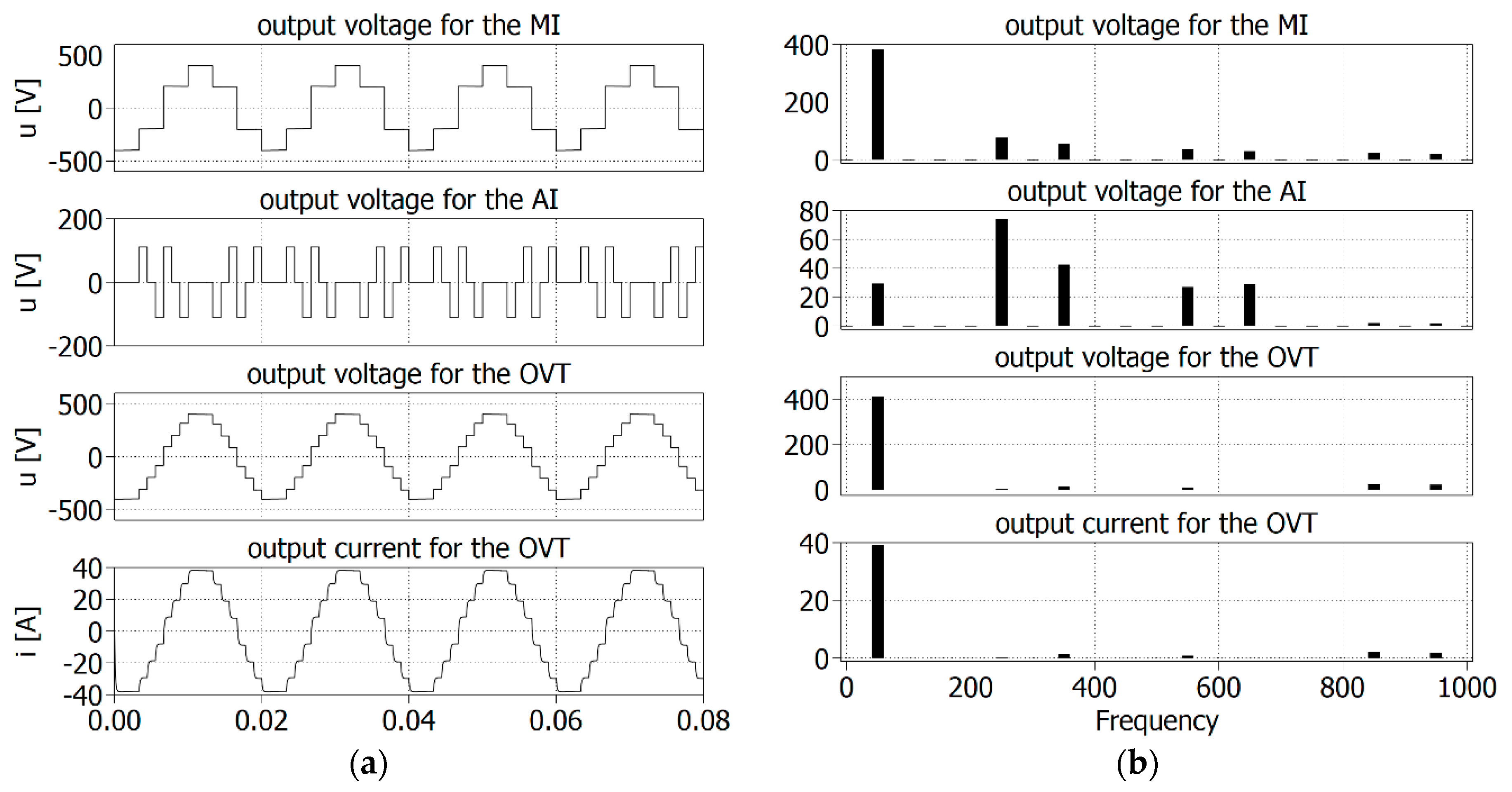
3. The Simulation and Experimental Studies for a Basic Version of the OVT Inverter
The basic simulation studies were carried out using the PLECS program. The control of the primary and auxiliary inverters was carried out using the vectors shown in
Figure 3. The simulation studies were performed for the model shown in
Figure 4. Then, experimental tests (
Figure 5) were carried out for a similar configuration of the inverters in the laboratory of the Electrotechnical Institute in Gdansk. In both the simulation and experimental studies, we used a power supply in the DC circuit equal to 400 V. Meanwhile, the values for the resistance and inductance of the load were defined as shown in
Table 1. A transformer in the “triangle-star” arrangement was used as a node summing the waveforms of both the inverters. The windings, connected in a delta configuration, constituted the load of the auxiliary inverter, and the secondary windings were connected in series to the load circuit. For this reason, the space vector of the auxiliary inverter is perpendicular to that of the main inverter, and the orthogonality condition was met.
The values of the R-L components used in this trial are summarized in
Table 1.
The main results, in the form of the THD and RMS coefficient for the main inverter output voltage (u
MI), voltage (u
OVT), and current (i
OVT) output for the orthogonal inverter are given in
Table 2.
A laboratory model of the converter was built for the experimental study. The following figures show the results of the testing a 40 kW converter. The control of the OVT converter was provided by an algorithm loaded on a DS1102 card from dSPACE with a TMS320C31 floating point signal processor. The voltage in the intermediate circuit U
D, measured at the full load of the converter, was 540 V. Measurement values and voltage waveforms were measured using LEM-type measuring transducers with a rated transmission of 500 V/5 V. Currents were measured by means of LEM-type measuring transducers with a gear ratio of 25 A/5 V. The phase voltage oscillogram of the main inverter MI is shown in
Figure 6, and the output phase voltage of the whole OVT converter is shown in
Figure 7.
The output voltage of the converter is slightly distorted in relation to the “pure” orthogonal waveform resulting from the theory. This is because it was not possible to select identical elements of an appropriate value in all phases of the measuring system and at the required power level. Here, the shape of the phase waveforms was determined by the ratio of the transformer connecting the inverters.
Figure 8 shows an oscillogram of the recorded waveforms of the phase currents generated by the OVT inverter in all phases. The load of the converter consisted of resistors and chokes. Their values are given in
Table 1. The load was connected in a star configuration.
The peaks in
Figure 6,
Figure 7 and
Figure 8 are typical measuring disturbances, which were gained during the laboratory experiments. These disturbances are superimposed on the measuring cables. A more extensive description of the experimental results of the OVT converter is given in the works reported in [
27,
28]. The experimental measurement setup is shown in
Figure 9.
4. Auxiliary Inverter Control Strategies Leading to the Transformer Power Reduction
The space-vector-controlled OVT inverter shown in
Figure 3 is characterized by its creation of an output stepped voltage containing significantly less higher harmonics than the typical three-phase VSI inverter controlled in the simplest way, as in the case of the main inverter (MI). However, the further analysis of the control vectors of the auxiliary inverter (AI) offers the possibility of reducing the power of the transformer used to connect both inverters. The authors of this paper proposed three solutions contributing to the reduction in the transformer power. All the proposed solutions involve changing the set of active vectors controlling the auxiliary inverter. For this purpose, three modulators were proposed. According to their dependence on the applied carrier signal, they are called: rectangular, triangular, and PWM. The proposed solutions are very simple in terms of their concept and implementation, which adds to the benefits of this approach.
Figure 9 shows the concept of the modification of the control circuits of the auxiliary inverter.
Using the simulation test workstation shown in
Figure 10, experiments relevant to the operation of the inverter were performed using the modulation systems shown in
Figure 11.
The workstation presented in
Figure 10 includes a computer with the PLECS software, a computer device for performing HIL (hardware-in-the-loop) simulations, and an oscilloscope for presenting the experimental results. The RT Box1 from PLEXIM was used as the HIL simulator during the study. The main simulation is carried out using the RT Box. A model created in PLECS is downloaded to the RT Box. The oscilloscope shown in
Figure 10 allows for the verification of the signals obtained during the simulation tests.
Figure 12a–c shows the modified modulator systems for the auxiliary inverter with the standard settings in the tested model.
Based on the waveforms and amplitude spectra shown in
Figure 13,
Figure 14 and
Figure 15, the operation of the inverter with the proposed modulator systems was documented. These tests were performed for the RL loads, with the values shown in
Table 1. These loads were also used during the experimental studies. The following simulation studies considered the basic cases of the inverter and control systems, thus forming the main theme in this article. There are plans to conduct further works aiming to implement algorithms using the DSP microprocessor and inverters.
It is important to note that, when using the applied carrier signal as a rectangular, triangular, or PWM generator, it is necessary to evaluate the level of the transformer output voltage.
Table 3 presents a summary of the RMS and THD parameters for the OVT, MI, and AI inverter voltages and currents under different AI inverter control strategies, with R = 2 ohms and L = 20 mH load.
The obtained results show that the three proposed methods of control allow us to obtain very acceptable and comparable results. The THDI factor of the current flowing through the resistive-inductive load is very low. Therefore, the proposed OVT inverter seems to be a very good device that is able to realize the DC/AC conversion process. As a grid-connected interface device, the OVT inverter has several advantages compared to other solutions.
The main advantage of the introduced modification of the control is that, compared to the basic control strategy, the proposed solutions allow for the reduction in the transformer ratio and, in the case of the system’s implementation, they contribute to reducing the transformer’s power and its size. In the basic version of the control (shown in
Figure 4), the transformer (N
MI: N
AI) had a winding ratio of 100:21, and after the introduction of the modified auxiliary inverter control, the ratio was 69:21.
The inevitable effect of the modulation strategies used for the auxiliary inverter is a marked increase in the content of higher harmonics of the AI voltage, while the OVT inverter significantly reduces the output voltage THD factor. The level of higher harmonics of the OVT output current is also significantly reduced.
5. Conclusions
The proposed modified OVT inverter is suitable for the realization of an effective DC/AC conversion process. Its operation, due to the introduced modifications, makes the inverter appropriate as a grid-connected interface device. The total power of the OVT inverter may be very high, but the power of the auxiliary one remains relatively low. According to the OVT concept, the power losses of both inverters are very low. The main inverter MI is switched only six times in one period of the voltage fundamental harmonic and power losses of the AI, equating to approximately just 5% ÷ 7% of the MI losses, dependent on the transformer ratio. Thus, the ratings of all the AI semiconductor devices are significantly lower. The simulation results prove that the AI inverter operates as a very effective active filter of the stepped voltage generated by the MI (main inverter).
The introduced modification of the control method allowed to adjust the transformer ratio. The frequency of the carrier signal should be high in order to reduce the transformer’s overall dimensions. The method of the AI control have a great influence on the THDI factor. Therefore, the control circuit of the complete OVT inverter can operate in the simplest way. The AI inverter operates as a very effective active filter of the stepped voltage generated by the MI (main inverter).
The results obtained during the simulation and experimental tests met the limit values of the EN: 50160 standard [
29].


