Article

An Improved Charge-Based Method Extended to Estimating Appropriate Dead Time for Zero-Voltage-Switching Analysis in Dual-Active-Bridge Converter

1
Graduate School of Pure and Applied Sciences, University of Tsukuba, Tsukuba 305-8573, Japan
2
Faculty of Pure and Applied Sciences, University of Tsukuba, Tsukuba 305-8573, Japan
*
Authors to whom correspondence should be addressed.
Energies 2022, 15(2), 671; https://doi.org/10.3390/en15020671
Submission received: 19 October 2021 / Revised: 12 December 2021 / Accepted: 12 January 2022 / Published: 17 January 2022
(This article belongs to the Special Issue Power Converters: Modeling, Design and Applications)

Abstract

:
This paper presents a comprehensive analysis of zero-voltage-switching (ZVS) realization with an improved charge-based method by considering both voltage dependency parasitic capacitance and dead time in dual-active-bridge (DAB) converters, when the voltage ratio between the primary and secondary sides does not match the turn ratio of the transformer. For this purpose, a unified equivalent circuit is proposed to represent the switching motions at all possible switching instances under the condition of one-leg manipulation. The combinations of switching cases can be presented in a table to build the corresponding equivalent circuit for ZVS analysis. Combined with the improved charge-based method, the common solutions of the minimum required switching current and the appropriate dead-time range for each equivalent circuit to realize ZVS are deduced. The allowable range of the dead time for ZVS as a function of the switching current is analyzed to determine the appropriate dead time. Once the switching current and dead-time range are derived, the model-based lowest switching current control method can be used to achieve ZVS by using the appropriate amount of both factors. Experiments using a 4 kW DAB prototype were conducted to verify the theoretical analyses.

1. Introduction

Over recent years, the dual-active-bridge (DAB) converter has been widely studied as an interface converter for various applications that require galvanic isolation, a high-voltage step-up/-down ratio, and bidirectional power flow control [1,2,3], for example, in vehicle-to-grid (V2G)-capable electric vehicle (EV) chargers, solid-state transformers (SSTs), and supercapacitor-based energy storage systems. By applying the conventional modulation method, the single-phase-shift (SPS) method, the DAB converter can easily achieve zero-voltage switching (ZVS) when the voltage ratio is fixed at its designated value without additional circuitry [4]. ZVS realization can effectively reduce the switching losses and electro-magnetic interference (EMI) emissions, especially for the areas where high-switching frequency converters are widely applied [5]. Moreover, ZVS operation can also reduce the risk of malfunction and the breakdown of power devices [6]. As another method of soft switching, zero-current switching (ZCS) is also an important technique in the research of bidirectional converters [7]. However, certain switching losses are still generated during the turning-on process compared with ZVS in a DAB converter. Thus, the research on ZVS in DAB converters has received much attention.
In some applications, such as energy storage using batteries and supercapacitors, and power conversions for an active power decoupling [8], a varying input voltage can be applied. However, once the input voltage deviates from the desired value, ZVS operation can be lost in some parts of the operation range. To address the above problem, many studies have been conducted over the past decade. A switched auxiliary inductor to change the equivalent magnetizing inductance has been proposed for extending the ZVS range in [9]. One of the drawbacks of this method is that additional components are needed; therefore, the power density can be reduced. Another major approach is using the so-called burst mode [10,11,12]. However, the switching transients present at the exchanging of the active and inactive periods cannot realize ZVS. In similar approaches, some modulations using a variable switching frequency have been proposed in [13,14,15]. Increasing the switching frequency can extend the range of ZVS in low-power operations. However this extension cannot be infinitely increased and the other losses related to the frequency can be increased. In addition to the above methods, ZVS-range extensions based on some advanced modulation strategies, such as an extended-phase shift (EPS), a dual-phase shift (DPS) and a triple-phase shift (TPS), by introducing a higher degree of freedom, have been introduced in [16,17,18,19,20].
Most research [12,13,14,16,17,18,19,20] discusses the switching condition to judge the ZVS under a current-based method, in which the current direction at the switching instant is simply used to judge whether the switching is ZVS or not. A charge-based method is much more precise method than the current-based method [21,22]. It judges ZVS considering if the charge stored in the parasitic capacitance of switches has totally been released before the switches turn on. With this method, the actual switching current needed to complete the ZVS can be obtained. Based on this approach, some works have proposed controlling the critical switching current for ZVS with optimized operations from certain aspects [21,23]. Moreover, an improved charge-based method, which considers the non-linearity of the parasitic capacitance of semiconductor devices, has been introduced. In [24], the ZVS judgement, in particular, the operating conditions of the EPS, is analyzed with the improved charge-based method. This can provide a much more accurate estimation of the required switching current to ensure the ZVS.
However, the switching current is not the sole required condition to achieve ZVS. An appropriate dead time is also needed. The charge-based method with considering the non-linear parasitic capacitance can estimate the process during the dead time accurately; however, it has not been applied to discuss the appropriate dead time in terms of ZVS realization. A strategy to determine the dead time, including the margin for possible error and a method to realize ZVS in actual converters, is a beneficial topic that will be discussed later on in this paper.
This paper applies the improved charge-based method, which considers the voltage dependency of the parasitic capacitance of devices, to discuss the appropriate dead-time period. For this purpose, a unified equivalent circuit used to consider all the possible switching conditions and any phase-shift modulations is proposed for the first time. Based on the equivalent circuit, the equation of the minimum required switching current to ensure ZVS is deduced. Then, a comprehensive analysis on characteristics of dead time is performed and the acceptable dead-time range as a function of the switching current is discussed so that strategies to determine the dead time can be discussed.
A 4 kW laboratory prototype of the DAB converter was used to verify the above theoretical research. The model-based lowest switching current control proposed in [23] for EPS was taken as an example to verify the appropriate dead-time period with enough of a margin of the switching current for ZVS.

2. Unified Equivalent Circuit for Switching Instant in DAB Converters

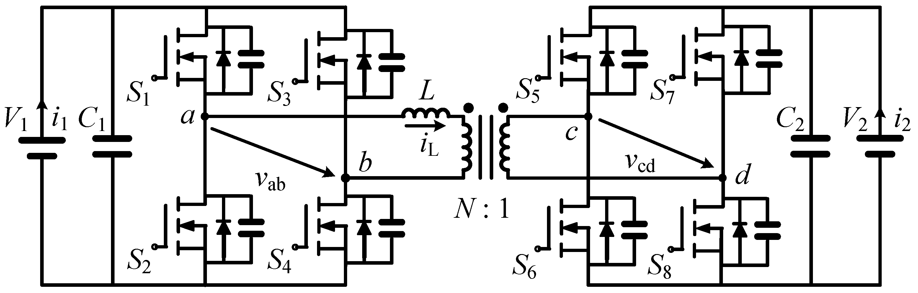
2.1. Model of Dual-Active-Bridge Converter

The configuration of the DAB converter is shown in Figure 1. The DAB converter consists of two H-bridges and a medium-frequency transformer (MFT) with a turn ratio of N : 1 . V 1 and V 2 are the DC terminal voltages of the input and output. L is the primary-side referred equivalent inductance of the transformer. The voltage ratio is defined as k = V 1 / ( N V 2 ) . The power devices are operating under the switching frequency of f sw .
Phase-shift modulations are the most widely used modulation techniques in DAB converters. Schematic waveforms of three typical methods, SPS, EPS and TPS, are shown in Figure 2. S 1 S 8 are the gate signals for the corresponding switches in Figure 1. In all the modulations, switches are controlled by 50% duty ratio signals and the phase-angle differences between them are controlled. Using different phase-shift relationships of gate signals, two- or three-level square voltages are generated in the port voltages of two full bridges, v ab and v cd . All the possible patterns to achieve cyclic and symmetric port voltages can be classified into three modulation schemes.
The schematic waveforms with SPS, which have a two-level port voltage on both sides, are shown in Figure 2a. The phase-shift difference between the two-level port voltage is expressed by its per-unit value as D δ and it is the sole control freedom in SPS for controlling power. In EPS, a three-level voltage is involved on one side, as shown in Figure 2b. Thus, another phase-shift ratio expressed as D f is introduced to this side. TPS is the most general modulation, which has a three-level voltage on both sides. The inherent phase-shift ratios in the primary and secondary sides are expressed as D fp and D fs , respectively. Thus, SPS and EPS are unique cases of TPS.

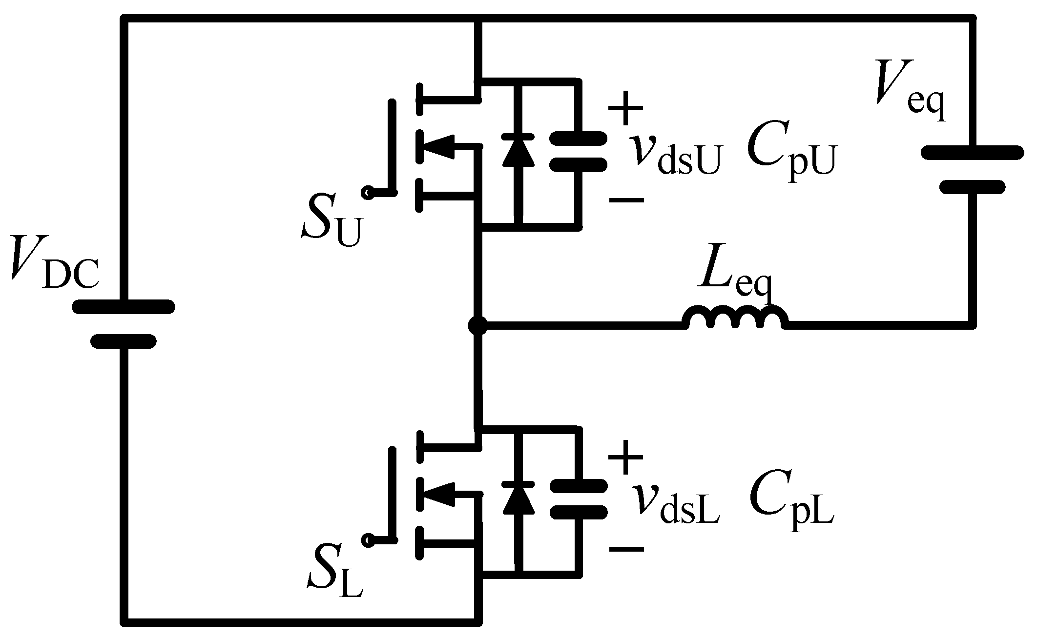
2.2. Unified Equivalent Circuit

To analyze ZVS realization, all the switching instants that cause changes in the port voltages should be analyzed. In any switching instances, only one or two legs are manipulated, while the others are kept as they are. The conditions where two legs are manipulated at the same time only happen in SPS and EPS.
A unified equivalent circuit, as shown in Figure 3, can be used to analyze all the possible switchings in the above modulations. The considered leg is composed by upper and lower devices, S U and S L , respectively. V DC is the DC terminal voltage of the operating side. V eq is the equivalent voltage source that represents the port voltage of the other side bridge converted to the operating side, V port . It should be mentioned that V port is equal to N v cd , which can be + N V 2 , N V 2 and zero, for considering the primary-side bridge, and v ab / N , which can be + V 1 / N , V 1 / N and zero, for considering the secondary-side bridge. Then V eq is determined in accordance with the status of the other leg in the same bridge, and can be + V port or V port . L eq is the equivalent series inductance converted to the operating side.
The leg which connects to the positive pole of the port voltage is defined as the left leg, and the leg which connects to the negative pole of the port voltage is defined as the right leg.
All the possible combinations of the switching leg, switching motion, and other conditions are listed in Table 1, resulting in V eq in the unified equivalent circuit. The # in the left column represents the number of conditions. All the cases are divided into left-leg switchings and right-leg switchings; the switching motion, status of the adjacent leg and V port are three decisive factors. By using these three factors, V eq in the unified equivalent circuit can be picked from the table. The connection of the equivalent circuit shown in Figure 3 corresponds to the conditions in which the upper switch in the adjacent leg of the considered bridge is kept on; therefore, V eq in these conditions can be directly obtained by the decisive factors and is shown in Table 1.
On the other hand, the cases in which the lower device in the adjacent leg is kept on cannot directly be explained by the circuit shown in Figure 3; however, the switching process of all these can be explained by any one of the cases with the upper switch on in the adjacent leg owing to the symmetry of the circuit. The counterparts of these cases are described in Table 1. The counterpart case has the complete opposite conditions of the three decisive factors in the same switching leg of the considered case. It should be mentioned that the corresponding direction of the inductor current is also the opposite in this case. It can be said that the opposite switching motion with the opposite current direction achieves the same switching process with the considered case, but the roles of upper and lower devices are changed. Consequently, all the possible switching instances that can happen in DAB converters can be explained by the unified equivalent circuit shown in Figure 3, picking V eq from Table 1 for the decisive factors.
For instance, at the t 1 instant of TPS in Figure 2c, the lower device S 4 turns on and the upper device S 3 turns off in the right leg. In the adjacent leg, the lower device S 2 is kept on. Meanwhile, the port voltage on the opposite side, V port , is negative. Thus, the switching at t 1 corresponds to case #23. As shown in the table, the counterpart case of #23 is #13, in which the upper device turns on in the right leg, the upper device in the adjacent leg is kept on and V port is positive. Since the upper device in the adjacent leg is kept off in #23, the t 1 instant cannot be explained by the given circuit directly. However, the switching process of #23 can be completely explained by its counterpart case, #13. Thus, the switching transient that happens at t 1 can be explained by the unified equivalent circuit with conditions described for case #13, that is, V eq = + V port = N V 2 .
It should be mentioned that the above discussion only involves the condition where one leg has switching motion. In SPS and EPS modulations, the conditions where two legs are manipulated simultaneously also existed; for instance, the switching at t 1 in SPS shown in Figure 2a and the switching at t 2 in EPS shown in Figure 2b. However, these conditions in EPS are usually not the critical switchings for ZVS. When these conditions become the critical switchings in SPS, other advanced modulations are usually used to take the place of SPS. Therefore, the conditions with one leg being manipulated are focused on in most of studies for ZVS in DAB converters and this paper does not pay much attention to the analysis of the conditions with two legs being manipulated.

3. Improved Charge-Based Method and Dead-Time Estimation

3.1. Concept of Minimal Switching Current

The most fundamental condition for realizing ZVS by the current-based method is the current direction at turn-on switching being negative (source to drain). Thus, the corresponding direction of the inductor current at the switching instant can be a sole judgement factor for ZVS. However, in practical converters, the parasitic capacitance and snubber capacitors connected to the devices in parallel need to be discharged by the end of the dead time to achieve ZVS. Therefore, the time for discharging and the dead time should be considered to judge the ZVS. This paper introduces a method considering both aspects. The improved charge-based method is extended to estimate the appropriate dead time.
With the knowledge introduced in the last section, all the switching instances under the condition of one leg being manipulated in DAB converters can be explained by the unified equivalent circuit in Figure 3. Furthermore, all of these switching instants can be classified into two cases in equivalent circuits where the upper device, S U , is turning on or the lower device, S L , is turning on. The circuits of these two cases are shown in Figure 4. The correct current direction to achieve ZVS based on the current-based method is assumed at the beginning of the dead time, and the current paths for the charging and discharging of the parasitic capacitance are drawn as dashed lines in the circuit diagrams with the direction.
The voltages across S U and S L are defined as v dsU and v dsL , respectively. In the action shown in Figure 4a, for instance, C pU is charged at the dc-side voltage; therefore, v dsU = V DC , and v dsL = 0 at the beginning of the process. Then, v dsL is increased by charging C pL and v dsU is decreased by discharging C pU when the direction of the inductor current is the right direction. After a certain period, the charging and discharging are completed. To achieve a zero-voltage turning-on of S U , it should be turned on after v dsU becomes zero. After v dsU becomes zero, the remaining current flowing through the inductor conducts through the free-wheeling diode of S U for a while. To achieve ZVS, S U should be turned on during this period, where v dsU is kept at zero. A similar derivation can be obtained for the case where S L is turned on with the current direction shown in Figure 4b. To ensure the remaining current flows through the body diode after the charging and discharging, a certain amount of the initial current in the inductor is indispensable.
This paper involves a concept of minimal switching current, I m , that is the minimum required current flowing through the inductor at the beginning of the dead time to complete the charging and discharging. With this current at the beginning of the dead time, the inductor current becomes exactly zero when the charging and discharging process is completed. With this condition, the end of the dead time can only be set at the instant when the inductor current reaches zero. Both longer and shorter dead times than this result in losing ZVS.

3.2. Derivation of Minimal Switching Current

Here, the case shown in Figure 4a with S U turning on is taken as a representative case in the following analysis. Considering the energy conservation in the equivalent circuit, the initial energy stored in the parasitic capacitance of the devices and the inductor should be equal to the sum of the final energy stored in them and the energy transferred to dc voltage sources. By assuming that the same type of devices are used for both the upper and lower arms, the electrostatic energy stored in C pU at the beginning of the instant is totally equal to that in C pL at the end; therefore, these parts can be canceled. If the initial inductor current is equal to the minimal switching current I m , the magnetic energy stored in the inductor becomes zero at the end of the transient; therefore, the initial magnetic energy in the inductor is equal to the energy transferred to the voltage sources as
1 2 L eq I m 2 = E dc ,
where E dc is the energy transferred to two dc voltage sources during the charging and discharging process.
The equivalent circuit shown in Figure 4a represents the case of upper device, S U , turning on. E dc in this condition, E dc ( S U _ on ) , can be derived as
E dc ( S U _ on ) = t a t b V DC i CL ( t ) + V eq i L ( t ) d t ,
where i CL and i L are the currents flowing through the dc voltage sources V DC and V eq , respectively. t a and t b are the time of the beginning and the end of the charging and discharging, respectively. In the equivalent circuits, the direction of V eq represents the polarity when the equivalent port voltage on the other side bridge takes positive. i L can be derived as
i L ( t ) = i CU ( t ) + i CL ( t ) ,
where i CU is the discharging current of C pU and i CL is also the charging current of C pL . i CL and i CU can be expressed as
i CL = C pL ( v dsL ) d d t v dsL = C p ( v dsL ) d d t v dsL , i CU = C pU ( v dsU ) d d t v dsU = C p ( V DC v dsL ) d d t v dsL ,
where C p is a universal expression for parasitic capacitance; therefore, S U and S L can be represented by the same function of C p . C p is usually a function of its drain–source voltage. As a result, the inductor current can be expressed as
i L = C p ( v dsL ) + C p ( V DC v dsL ) d d t v dsL .
The total transferred charge by i CL and i L are defined as Δ Q CL and Δ Q L , respectively, and can be calculated as
Δ Q CL = t a t b i CL ( t ) d t = 0 V DC C p ( v ) d v , Δ Q L = t a t b i L ( t ) d t = 0 V DC C p ( v ) + C p ( V DC v ) d v .
In general, the transferred charge through a device with the voltage charging from 0 to V can be expressed as
Q ( V ) = 0 V C p ( v ) d v ,
and its value can usually be obtained from device data-sheets. By using (7), Δ Q CL and Δ Q L in (6) can be expressed as
Δ Q CL = 0 V DC C p ( v ) d v = Q ( V DC ) , Δ Q L = 0 V DC 2 C p ( v ) d v = 2 Q ( V DC ) ,
By using (6) and (8), (2) can be rewritten as
E dc ( S U _ on ) = 0 V DC V DC C p ( v ) + 2 V eq C p ( v ) d v = ( V DC + 2 V eq ) Q ( V DC ) .
I m for the case of the upper device turning on, I m ( S U _ on ) , can be derived as
I m ( S U _ on ) = 2 E dc ( S U _ on ) L eq = 2 ( 2 V eq V DC ) Q ( V DC ) L eq .
When the practical voltage ratio of 0.5 < k < 2 and V eq = + V port , which gives 2 V eq V DC > 0 , is assumed, E dc ( S U _ on ) > 0 is achieved. For example, case #13 in Table 1 can be a representative of this condition. On the contrary, when V eq = V port , as is the case of #14, E dc ( S U _ on ) < 0 is achieved. It is obvious that, when E dc ( S U _ on ) < 0 , a valid I m ( S U _ on ) is not available.
The same derivation can be performed in the equivalent circuit shown in Figure 4b with S L turning on. The energy transferred to the voltage sources of the equivalent circuit for the case of the lower device turning on, E dc ( S L _ on ) , and the minimal switching current in this condition, I m ( S L _ on ) , can be derived as
E dc ( S L _ on ) = 0 V DC V DC C p ( v ) 2 V eq C p ( v ) d v = ( V DC 2 V eq ) Q ( V DC ) ,
and
I m ( S L _ on ) = 2 E dc ( S L _ on ) L eq = 2 ( V DC 2 V eq ) Q ( V DC ) L eq .
When the practical voltage ratio of 0.5 < k < 2 and V eq = + V port , as is the case of #1, for instance, which gives V DC 2 V eq < 0 , E dc ( S L _ on ) < 0 is achieved. On the contrary, when V eq = V port , as is the case of #20, E dc ( S L _ on ) > 0 is achieved. Additionally, when E dc ( S L _ on ) < 0 , a valid I m ( S L _ on ) is not available.
In conclusion, all of the possible switching instances with one-leg manipulation can be classified into two categories: E dc > 0 and E dc < 0 . The schematic and example waveforms of the drain–source voltages and the inductor current with a long enough dead time for these two categories are shown in Figure 5. E dc > 0 means that the dc voltage sources receive energy from the inductor; therefore, the current at the end of the charging and discharging process becomes closer to zero than that at the beginning, as shown in Figure 5a. This clearly indicates that a certain positive value of I m is needed to complete the charging and discharging with this current, where the positive value for I m means the correct direction for ZVS based on the current-based method. On the other hand, E dc < 0 means that the dc voltage sources give out energy to the inductor; therefore, the current at the end of the charging and discharging process becomes farther from zero than that of the beginning as shown in Figure 5b. Hence, even zero initial current can realize ZVS and any correction for ZVS in practical condition is not needed. That is the reason why I m does not have an available solution in the case of E dc < 0 .

3.3. Lowest Switching Current Control

Once I m at a specific switching instant is deduced, a strategy called lowest switching current control, which is proposed in [23], can be used to control the current at this instant to be equal to a given reference, which is defined as I m * . This is a modification of the conventional modulations that manipulates the current at some switching instances slightly based on the model of the circuit with known parameters. This method is only available for the modulations which have two or more degrees of control freedom, such as EPS and TPS, since the switching current must be modified without changing the transferred power. At the very least, I m * > I m is needed. In addition, it should be mentioned that an appropriate margin should be included into I m * to ensure ZVS for both the possible control error of the lowest switching current and the variations in circuit parameters and operating conditions.

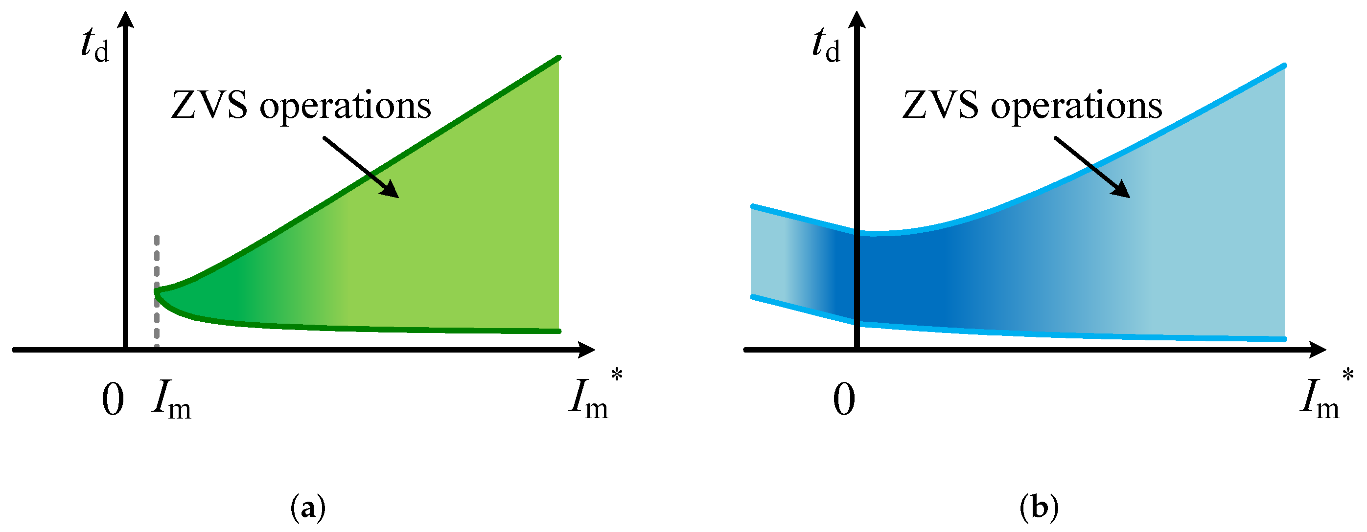
3.4. Range of Dead-Time Duration for ZVS

All the above analyses focus on the initial current value at the beginning of the dead time, t a . It is also important to discuss the end instant of the dead time. Here, we also took the two categories of E dc > 0 and E dc < 0 as different cases to analyze. It can be seen from the schematic waveforms shown in Figure 5 that the current conducts the free-wheeling diode of S U (or S L ) after the charging and discharging process is completed at t b . The switch voltages are clamped until i L reaches zero at t c . Consequently, the dead time should be ended between t b and t c , and the dead-time duration, t d , should be longer than t b t a and shorter than t c t a .
The allowable range of the dead time for ZVS depends on the initial current. This paper assumes that the initial current is successfully controlled to be equal to I m * . The range of the dead time can be a function of I m * . It is difficult to solve the charge and discharge duration algebraically; however, it is enough to analyze it by a numerical approach for the purpose of suggesting the appropriate dead time, since it only depends on the almost fixed circuit parameters, including dc source voltages and the characteristics of the parasitic capacitance.
Figure 6 shows the schematic view of the range of the dead-time duration, t d , for ZVS as function of I m * . There is a lower limit, which corresponds to t b t a , and an upper limit, which corresponds to t c t a . As discussed in Section 3.2, there is a certain positive value of minimal switching current, I m , under the condition of E dc > 0 . With this minimal switching current condition, the charging and discharging process is ended when the current reaches zero; therefore, the lower and upper limits become equal, as shown in Figure 6a. Consequently, there is no ZVS area below this initial current under E dc > 0 . On the other hand, there is no limitation related to the initial switching current under E dc < 0 , as shown in Figure 6b; therefore, the ZVS range still exists around zero initial current and even in the negative initial current range in principle. With the negative initial current, an extra time period before t a , in which the charging and discharging of the parasitic capacitance are not started, is included in the dead time. Therefore, both the lower and upper limits of the dead time linearly increased for as long as the increase in | I m * | , as shown in Figure 6.
The results shown in Figure 6 suggest that a wider range of dead-time durations to achieve ZVS can be available by setting a high value for I m * . Therefore, a large margin of I m * is good for ZVS realization in both aspects—enough of an initial switching current and appropriate dead-time value.
Furthermore, it can be found that the allowable range of t d for ZVS under the condition of E dc > 0 is narrower than that under E dc < 0 in general. This is due to the fact that | i L | decreases under E dc > 0 , while it increases under E dc < 0 , as can be seen from Figure 5. The narrower range of t d makes it more difficult for the switching under E dc > 0 to achieve ZVS than that under E dc < 0 .

4. Experimental Verification of ZVS Realization

4.1. Experimental Setup

To verify that the evaluation of ZVS by improved charge-based method and dead-time estimation is effective, a laboratory prototype of the DAB converter with the power rating of 4 kW was fabricated as shown in Figure 7. Table 2 shows the specifications of the fabricated DAB converter.
The DAB converter can be operated, for instance, in EPS modulation. It should be mentioned that, in other modulations, operations with one-leg manipulations will achieve the same results. The switching instant at t 4 of EPS, as shown in Figure 2b, is the critical switching. The critical switchings in the condition of k < 0 and k > 0 exactly correspond to cases #13 and #8 in Table 1. Two different settings of the voltage ratio, k = 0.67 and k = 1.5 with the power flow from the primary to secondary side, which represent the condition E dc > 0 and E dc < 0 , respectively, are taken as examples.

4.2. Estimation of Minimal Switching Current and Dead-Time Range for ZVS

To verify the feasibility of the proposed method for ZVS realization in the practical condition, the lowest switching current control was tested in the fabricated converter. Prior to the experiments, the minimal switching current, I m , and the dead-time range for ZVS with the parameters of the fabricated converter were estimated in both settings. As discussed in Section 3.2, the constraint of the minimum switching current exists in the condition of E dc > 0 , with V DC = 400 V, and Q( V DC ) can be calculated as 137 nC by using (7) and the C–V characteristics of the device. Thus, the theoretical minimal switching current, I m , for k = 0.67 is calculated as 0.8 A by using (10). Due to the dc voltage giving out energy to the inductor in the condition of E dc < 0 with V DC = 400 V, I m = 0 A is assumed in this paper without any correction for ZVS in the practical condition.
The lower and upper limits of the dead-time duration, t d , as a function of the initial switching current were also estimated. The estimation was performed numerically since the algebraic derivation of the duration is complicated. The numerical analysis was in the time domain and based on the given initial circuit parameters at the beginning of the dead time. It also considered the voltage-dependent parasitic capacitance, which is represented by the C–V characteristics of the device.
The estimation results of the dead-time range for both k = 0.67 and k = 1.5 are shown in Figure 8 as solid lines. Figure 8a also confirmed that the upper and lower limits meet at I m = 0.8 A.

4.3. Verification of ZVS Realization with Lowest Switching Current Control

4.3.1. Operations without Lowest Switching Current Control

To verify that the ZVS cannot be achieved without considering the parasitic capacitance and dead-time period, some operations with the initial switching current controlled to be zero were tested. These operating points are indicated in Figure 8 as A, B, and C. To observe the critical switching transients, the reference power was set at 2000 W for all the operations of A, B, and C.
The experimentally measured zoomed waveforms during the dead time of the critical switching transients are shown in Figure 9. These include the drain–source voltage of the device to be turned on, v dsU in Figure 9a, v dsL in Figure 9b,c, the transformer current, i L , and the gate signals for S U and S L instead of the gate–source voltages. It can be seen that the converter did not achieve zero voltage turn-on at those switching transients. In operation A, in which the initial switching current is equal to zero under E dc > 0 , the discharging of v dsU was not completed by the time that i L becomes zero; therefore, there was no chance of achieving ZVS, even by controlling t d . In operation B, in which t d is lower than the lower limit under E dc < 0 , the discharging was slowly continuing with increasing i L ; however, there was not enough dead time to complete the discharging. In operation C, in which t d was higher than the upper limit, the dead time was too long so that the recharging of v dsL was observed.

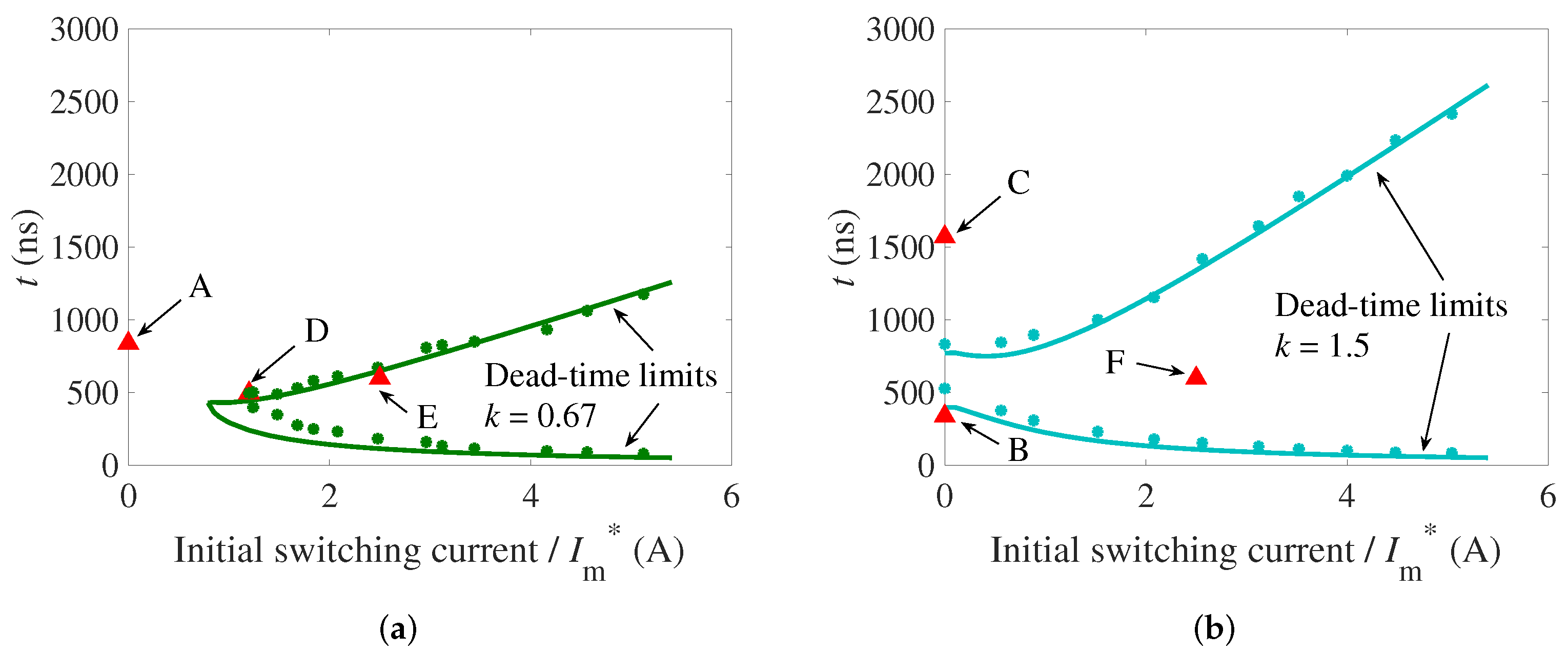
4.3.2. Verification of Dead-Time Range for ZVS

To verify the theoretical calculation of the limits, the boundary operations of the ZVS were searched experimentally. Specifically, the lower and upper limits of t d were identified by observing the waveforms when changing the initial switching current. During the experiments, the reference powers were set at 2000 W for both k = 0.67 and k = 1.5 . The experimentally observed lower and upper limits of t d for k = 0.67 and k = 1.5 are shown in Figure 8 as marks. The trend of experimental results agreed with the calculated boundaries. Both the calculated and experimental results verify that the dead-time range in E dc > 0 is narrower than that under E dc < 0 . It is much easier to achieve ZVS with a wide dead-time range under the condition of E dc > 0 .
The operating point with the experimental minimal switching current in E dc > 0 was found at the point of I m = 1.2 A and t d = 500 ns, and is marked as D in Figure 8a. The zoomed waveforms during the dead time of one critical switching transient with this operation are shown in Figure 10. It can be observed from the waveforms that the discharging of v dsU was completed just at the moment when i L reached 0 A.

4.3.3. Operations with Lowest Switching Current Control and Designed Dead Time

To verify that the ZVS can always be achieved in the operations with a designed initial switching current and the dead time discussed in Section 4.2, two operating points under the lowest switching current control were tested. I m * were set as 2.5 A for both k = 0.67 and k = 1.5 considering margins for possible errors. On the other hand, a constant dead time, t d = 600 ns, was set for this setup to ensure that the switching condition is far enough from both limits for any initial switching current. Corresponding settings of I m * and t d are marked as E and F in Figure 8.
The zoomed waveforms of the critical switching transients of the operations with the power reference of 2000 W for both k = 0.67 and k = 1.5 are shown in Figure 11. It can be clearly seen that the drain–source voltage of the device to be turned on discharged completely and the polarity of i L did not change during the dead-time in both operations. Thus, it is confirmed that ZVS was successfully realized with enough of a margin for this setting.

5. Conclusions

This paper proposes a unified equivalent circuit to consider all the possible switching instants under the condition of a one-leg manipulation in DAB converters. By using the unified equivalent circuit, an improved charge-based method with dead-time estimation is studied to identify the ZVS realization considering the effect of both the voltage-dependent parasitic capacitance and dead-time period. All equivalent circuits can be divided into two cases, the upper or lower device turning on, and the corresponding equations of the specific initial current, which is defined as the minimal switching current, are deduced. With the different parameters of the circuit, all of the switching instants can be further classified into two categories according to the sign of the energy transferred to dc voltage sources. Based on the classification, the function of the acceptable dead-time range with a switching current is analyzed and different difficulties for realizing ZVS operations are found in these two categories. A laboratory 4 kW DAB prototype was fabricated to verify that the estimation of ZVS realization by an improved charge-based method is effective. The lowest switching current control when considering enough of a margin of the switching current and dead time can successfully achieve ZVS at critical switching instants. It is much easier to realize ZVS operation with a wider dead-time range by using the category of E dc < 0 . Thus, during the designing and operating of DAB converters, besides the margin of the switching current and dead time being considered, operations that satisfied E dc < 0 are welcomed for easier ZVS realization.

Author Contributions

Conceptualization, H.Z. and T.I.; methodology, H.Z.; software, H.Z.; validation, T.I.; formal analysis, H.Z. and T.I.; investigation, H.Z. and T.I.; resources, T.I.; data curation, H.Z.; writing—original draft preparation, H.Z.; writing—review and editing, T.I.; visualization, H.Z.; supervision, T.I.; project administration, T.I.; funding acquisition, T.I. All authors have read and agreed to the published version of the manuscript.

Funding

This research received no external funding.

Data Availability Statement

Not applicable.

Conflicts of Interest

The authors declare no conflict of interest.

References

  1. Inoue, S.; Akagi, H. A bidirectional isolated dc-dc converter as a core circuit of the next-generation medium-voltage power conversion system. IEEE Trans. Power Electron. 2007, 22, 535–542. [Google Scholar] [CrossRef]
  2. Grbovic, P.J.; Delarue, P.; Moigne, P.L.; Bartholomeus, P. A bidirectional three-level dc-dc converter for the ultracapacitor applications. IEEE Trans. Ind. Electron. 2010, 57, 3415–3520. [Google Scholar] [CrossRef]
  3. Zhao, B.; Song, Q.; Liu, W.; Sun, W. Current-stress-optimized switching strategy of isolated bidirectional dc-dc converter with dual-phase-shift control. IEEE Trans. Ind. Electron. 2013, 60, 4458–4467. [Google Scholar] [CrossRef]
  4. Chen, B.; Lai, Y. Switching control technique of phase-shift-controlled full-bridge converter to improve efficiency under light-load and standby conditions without additional auxiliary components. IEEE Trans. Power Electron. 2010, 25, 1001–1012. [Google Scholar] [CrossRef]
  5. Guidi, G.; Kawamura, A.; Sasaki, Y.; Imakubo, T. Dual active bridge modulation with complete zero voltage switching taking resonant transitions into account. EPE J. 2012, 22, 5–12. [Google Scholar] [CrossRef]
  6. Yan, Y.; Bai, H.; Yang, C.; Wang, W. Securing full-load-range zero voltage switching for a dual active bridge based electric vehicle charger. In Proceedings of the 2020 IEEE Applied Power Electronics Conference and Exposition (APEC), New Orleans, LA, USA, 15–19 March 2020; pp. 2067–2072. [Google Scholar]
  7. Qu, Y.; Shu, W.; Kuan, Y.; Chiang, S.; Chang, J. A low-profile high-efficiency fast battery charger with unifiable constant-current and constant-voltage regulation. IEEE Trans. Circuits Syst.-I Regul. Pap. 2020, 67, 4099–4109. [Google Scholar] [CrossRef]
  8. Akihiro, M.; Isobe, T.; Terazono, K.; Tadano, H. Unbalanced load compensation for solid-state transformer using smoothing capacitors of cascaded h-bridges as energy buffer. In Proceedings of the IECON 2019, 45th Annual Conference of the IEEE Industrial Electronics Society, Lisbon, Portugal, 14–17 October 2019; Volume 1, pp. 6779–6786. [Google Scholar]
  9. Higa, H.; Itoh, J. Extendsion of zero-voltage-switching range in dual active bridge converter by switched auxiliary inductance. In Proceedings of the 2017 IEEE Energy Conversion Congress and Exposition (ECCE), Cincinnati, OH, USA, 1–5 October 2017; pp. 5324–5331. [Google Scholar]
  10. Rodriguez, A.; Vázquez, A.; Lamar, D.G.; Hernando, M.M.; Sebastián, J. Different purpose design strategies and techniques to improve the performance of a dual active bridge with phase-shift-control. IEEE Trans. Power Electron. 2015, 31, 790–804. [Google Scholar] [CrossRef]
  11. Haneda, R.; Akagi, H. Design and performance of the 850-V 100-kW 16-kHz bidirectional isolated dc-dc conveter using SiC-MOSTEFT/SBD H-bridge modules. IEEE Trans. Power Electron. 2020, 35, 10013–10025. [Google Scholar] [CrossRef]
  12. Oggier, G.G.; Ordonez, M. High-efficiency DAB converter using switching sequences and burst mode. IEEE Trans. Power Electron. 2016, 31, 2069–2082. [Google Scholar] [CrossRef]
  13. Guidi, G.; Pavlovsky, M.; Kawamura, A.; Imakubo, T.; Sasaki, Y. Improvement of light load efficiency of dual active bridge dc-dc converter by using dual leakage transformer and variable frequency. In Proceedings of the 2010 IEEE Energy Conversion Congress and Exposition (ECCE), Atlanta, GA, USA, 12–16 September 2010; pp. 830–837. [Google Scholar]
  14. He, X.; Zhang, Z.; Cai, Y.; Liu, Y. A variable switching frequency hybrid control for ZVS dual active bridge converters to achieve high efficiency in wide load range. In Proceedings of the 2014 IEEE Applied Power Electronics Conference and Exposition (APEC), Fort Worth, TX, USA, 16–20 March 2014; pp. 1095–1099. [Google Scholar]
  15. Hiltunen, J.; Väisänen, V.; Juntunen, R.; Silventoinen, P. Variable-frequency phase shift modulation of a dual active bridge converter. IEEE Trans. Power Electron. 2015, 30, 7138–7148. [Google Scholar] [CrossRef]
  16. Oggier, G.G.; Leidhold, R.; Garcia, G.O.; Oliva, A.R.; Balda, J.C.; Barlow, F. Extending the ZVS operating range of dual active bridge high-power dc-dc converters. In Proceedings of the 2006 37th IEEE Power Electronics Specialists Conference, Jeju, Korea, 18–22 June 2006; pp. 1–7. [Google Scholar]
  17. Iyer, V.M.; Gulur, S.; Bhattacharya, S. Hybrid control strategy to extend the ZVS range of a dual active bridge converter. In Proceedings of the 2017 IEEE Applied Power Electronics Conference and Exposition (APEC), Tampa, FL, USA, 26–30 March 2017; pp. 2035–2042. [Google Scholar]
  18. Liu, B.; Davari, P.; Blaabjerg, F. An Optimized Control Scheme for Reducing Conduction and Switching Losses in Dual Active Bridge Converters. In Proceedings of the 2018 IEEE Energy Conversion Congress and Exposition (ECCE), Portland, OR, USA, 23–27 September 2018; pp. 622–629. [Google Scholar]
  19. Das, A.K.; Fernandes, B.G. Fully ZVS, minimum RMS current operation of isolated dual active bridge dc-dc converter employing dual phase-shift control. In Proceedings of the 2019 21st European Conference on Power Electronics and Applications (EPE’19 ECCE Curope), Genova, Italy, 3–5 September 2019; pp. 1–10. [Google Scholar]
  20. Calderon, C.; Barrado, A.; Rodriguez, A.; Alou, P.; Lazaro, A.; Fernandez, C.; Zumel, P. General analysis of switching modes in dual active bridge with triple phase shift modulation. Energies 2018, 11, 2419. [Google Scholar] [CrossRef] [Green Version]
  21. Xu, G.; Sha, D.; Zhang, J.; Liao, X. Unified boundary trapezoidal modulation control utilizing fixed duty cycle compensation and magnetizing current design for dual active bridge dc-dc converter. IEEE Trans. Power Electron. 2016, 32, 2243–2252. [Google Scholar] [CrossRef]
  22. Kasper, M.; Burkart, R.M.; Deboy, G.; Kolar, J.W. ZVS of power mosfets revisited. IEEE Trans. Power Electron. 2016, 31, 8063–8067. [Google Scholar] [CrossRef]
  23. Zhang, H.; Akihiro, M.; Mannen, T.; Isobe, T. An optimized scheme for current stress reduction with zero-voltage switching in dual-active-bridge converters under varying input voltage. In Proceedings of the 2020 IEEE Energy Conversion Congress and Exposition (ECCE), Detroit, MI, USA, 11–15 October 2020; pp. 1223–1230. [Google Scholar]
  24. Yan, Y.; Gui, H.; Bai, H. Complete ZVS Analysis in dual-active-bridge. IEEE Trans. Power Electron. 2020, 36, 1247–1252. [Google Scholar] [CrossRef]
Figure 1. Configuration of the dual-active-bridge (DAB) converter.
Energies 15 00671 g001
Figure 2. Schematic waveforms of the DAB converter with the (a) SPS modulation, (b) EPS modulation, and (c) TPS modulation.
Energies 15 00671 g002
Figure 3. Unified equivalent circuit of the DAB converter, in which all the possible switching instances can be analyzed.
Energies 15 00671 g003
Figure 4. Equivalent circuits for analyzing ZVS: (a) for S U turning on and (b) for S L turning on. The required initial directions of currents to achieve ZVS are also shown in the circuits.
Energies 15 00671 g004
Figure 5. Schematic waveforms of the drain–source voltages and the inductor current with a long enough dead-time period of critical switchings, (a) for the condition of E dc > 0 , and (b) for the condition of E dc < 0 .
Energies 15 00671 g005
Figure 6. Schematic view of the range of dead-time durations, t d , as function of I m * in the conditions of (a) E dc > 0 and (b) E dc < 0 .
Energies 15 00671 g006
Figure 7. Overview of (a) fabricated 4 kW experimental setup and (b) back side of the single DAB board.
Energies 15 00671 g007
Figure 8. Lower and upper limits of the dead-time duration for ZVS shown as solid lines, and experimentally measured boundary operating points shown as star marks in the conditions of (a) k = 0.67 ( E dc > 0 ), and (b) k = 1.5 ( E dc < 0 ). Some example operating points discussed in this section are marked as A, B, C, and D, and resulting settings for operations are marked as E and F.
Energies 15 00671 g008
Figure 9. Zoomed waveforms around critical switching transients with the operating points outside of dead-time range for ZVS as example points, (a) marked as A, (b) marked as B, and (c) marked as C in Figure 8.
Energies 15 00671 g009
Figure 10. Zoomed waveforms around critical switching transient with the operating point at the experimental minimal switching current indicated as point D in Figure 8a.
Energies 15 00671 g010
Figure 11. Zoomed waveforms around critical switching transients with enough margin of initial switching current and dead-time as example points (a) marked as E, (b) marked as F in Figure 8.
Energies 15 00671 g011
Table 1. List of all possible combinations of switching cases and the corresponding results of V eq in phase-shift modulations.
#SwitchingSwitchingDevice in V port V eq
LegMotionAdjacent Leg
1left upper on+ V port
2 + V port
3 S U turns on,00
4 S L turns offlower on+refer to #8
5 refer to #7
6 0refer to #9
7 upper on+ V port
8 + V port
9 S U turns off,00
10 S L turns onlower on+refer to #2
11 refer to #1
12 0refer to #3
13right upper on+ + V port
14 V port
15 S U turns on,00
16 S L turns offlower on+refer to #20
17 refer to #19
18 0refer to #21
19 upper on+ + V port
20 V port
21 S U turns off,00
22 S L turns onlower on+refer to #14
23 refer to #13
24 0refer to #15
Table 2. Specifications of 4 kW Prototype of DAB Converter.
Rated powerP4 kW
Switching frequency f sw 20 kHz
Input voltage V 1 270 V ( k = 0.67 )
400 V ( k = 1.5 )
Output voltage V 2 400 V ( k = 0.67 )
270 V ( k = 1.5 )
Leakage inductanceL61  μ H
Transformer winding ratio 1 : n 1 : 1
Type of devices C3M0025065D
Publisher’s Note: MDPI stays neutral with regard to jurisdictional claims in published maps and institutional affiliations.

