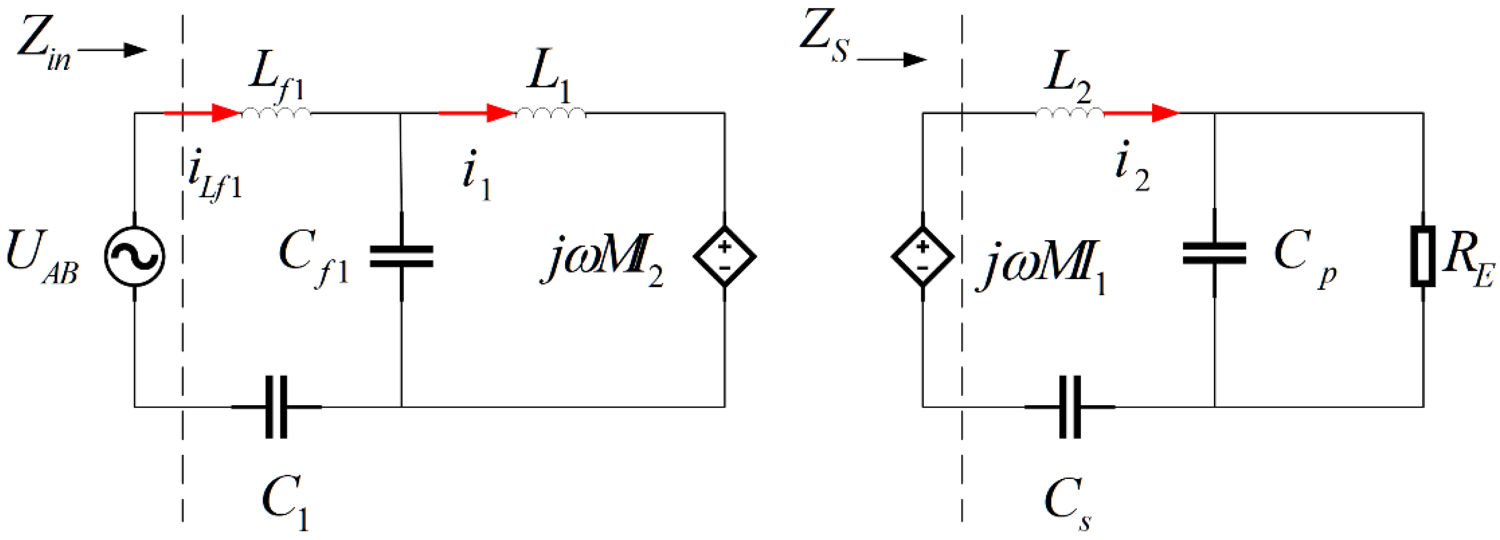
Article

A Self-Tuning LCC/SP System for Electric Vehicle Wireless Charging against Large Self- and Mutual Inductance Variations

1
Department of Automotive Engineering, Tongji University, Shanghai 201800, China
2
Engineering Department, Division B, University of Cambridge, Cambridge CB3 0FA, UK
*
Authors to whom correspondence should be addressed.
Energies 2022, 15(11), 3980; https://doi.org/10.3390/en15113980
Submission received: 23 April 2022 / Revised: 22 May 2022 / Accepted: 23 May 2022 / Published: 27 May 2022

Abstract

:
An LCC/SP self-tuning wireless charging system is proposed herein for use in a wireless charging test bench. With different dislocations in addition to changes in the coil self-inductance and mutual inductance caused by different secondary magnetic shielding materials, the system can ensure that the high power factor of the primary side remains unchanged without changing the circuit topology. Based on this normalized detuning LCC/SP circuit model, a switch-controlled capacitor (SCC) self-tuning method based on PI control is proposed. The control scheme employs only two MOSFETs and capacitors, without WIFI communication or parameter identification. A 2 kW experimental device was set up in the laboratory, and experimental verification was carried out with large-scale dislocations and different secondary magnetic shielding materials. The experimental results confirm that the system can maintain a high power factor (>0.9) under a system mutual inductance variation of 47.7% and secondary coil self-inductance variation of 12%, and that it can be applied in electric vehicle wireless chargers or high-power wireless charger test benches.

1. Introduction

In recent years, the use of wireless charging technology in electric vehicles has attracted increased academic and business attention due to its safety and convenience as well as the fact that it does not require electrical contact and involves low maintenance costs [1,2,3]. Thanks to the development of power electronics technology, wireless energy transmission technology has entered the realm of commercial promotion. However, coil dislocation caused by parking during the wireless charging of electric vehicles is ubiquitous and unavoidable, whereas this is not the case in consumer electronics applications, such as mobile phones. In addition, this system suffers from the influence of temperature on magnetic coupling structure parameters and the fragmentation of magnetic shielding materials caused by vehicle bumps, resulting from the presence of coil magnetic shielding materials. In the above cases, the self-inductance and mutual inductance parameters of the coil group will deviate from the initial value. The system will enter a non-resonant state, as the compensation parameters are no longer matched, thus affecting the regular operation of the wireless energy transmission system.
Electromagnetic induction wireless energy transmission systems have a typical loose-coupling structure, and their coupling coefficient is generally less than 0.3, so the considerable leakage of inductance that occurs within the transmitting and receiving coil does not result in energy transfer; the reactive power induced will instead reduce system transmission efficiency and increase device stress. This suggests that the resonant compensation topology used to compensate for the leakage inductance of the coil and improve the efficiency of the system is necessary during regular operation. According to the mode of connection between the compensation capacitor and the compensated coil, typical resonant compensation topologies are divided into four basic types: SS, SP, PP, and PS. Victor Shevchenko [4] conducted extensive analysis and comparison of the transmission characteristics and application scenarios of the four basic compensation topologies. The extended types include LCC/S, LCC/P, LCC/SP, and LCC/SP. In general, the ultimate purpose of the compensation topology of the primary side is to minimize the reactive power of the inverter output, and that of the secondary side’s compensation topology is to maximize the output capacity of the system.
In Table 1, the performance of resonant topology circuits commonly used for wireless energy transmission in electric vehicles is compared and analyzed. The simplest topologies are SS [5,6] and PP [7], wherein the primary and secondary sides of the system are connected in series and parallel with the coil via a compensation capacitor, respectively. These two topologies are low-cost, but their design freedom is low, and their transmission characteristics are sensitive to changes in the self-inductance of the coil. In PP compensation, the input impedance angle of the system is affected by the mutual inductance of the system, which necessitates the online adjustment of the impedance angle under different coil dislocations. In [8], the two simplest topologies are compared, and it is concluded that topology PP has the lowest efficiency. The impedance characteristics of various compensation topologies are also analyzed.
In [9], the resonant compensation topology of LCC/LCC is adopted, which has a high degree of freedom in its design. Its transmission performance is insensitive to fluctuations in the coil parameters and it has a robust anti-offset ability. However, the primary and secondary sides of the scheme require three additional compensation elements, respectively, which increase the design cost and the overall volume of the circuit.
LCC/S [10] and LCC/P [11,12] are relatively simplified resonant compensation topologies. Their primary sides employ the LCC compensation method, while their secondary sides employ series or parallel methods to compensate for the secondary side coil. Yafei Chen [13] compares the simplest SS topology with the LCC/S topology. It is pointed out that LCC/S topology is more suitable in the low power range, SS topology is more suitable in the high power range, and SS topology is more sensitive to load. Under rated resonance, the input-side impedance angle of LCC/S does not change with the mutual inductance of the coil, which means it can be applied in the wireless energy transmission of electric vehicles. However, its secondary side employs only one compensation element, so the voltage stress on this element is high. In addition, the topology involves a constant output of voltage on the secondary output side, which makes the direct connection of the battery load unsuitable. Compared with the LCC/S, the LCC/P compensation topology has a constant current output on the secondary side, implying that it can directly charge the battery load. However, its secondary side still employs a resonant parallel compensation element; therefore, current stress on this element is relatively large.
In [14], Yiming Zhang proposed an LCC/N topology in which there are no resonant components on the second side, which greatly reduces the cost, and no fixed output characteristics. The CC/CV characteristics of the output are realized by adjusting the input voltage, which is suitable for wireless charging systems with high power.
Therefore, a resonant topology circuit of LCC/SP is proposed in [15,16]. Two compensation elements are used on the secondary side of the circuit, allowing the voltage and current stress on the element to be effectively shared. At the same time, the resonant topology circuit has a good harmonic suppression ability and enables a constant current output, which simplifies the design of the secondary circuit to a certain extent. Therefore, this work focuses on the LCC/SP resonant compensation circuit. The LCC/SP topology’s input impedance angle is closely related to the mutual inductance of the coil, so an additional impedance angle adjustment device is required.
Table 1. Performance comparison of typical topologies.
Topology SS [5,6]PP [7,8]LCC/S [10,13]LCC/LCC [9,17,18]LCC/P [11,12]LCC/SP [15,16]LCL/N [14]
Items
Number of compensation elements on secondary side1113120
Cost and sizeLowLow MediumHighMediumMediumLow
Degree of design freedom0012120
Harmonic suppression capabilityWeakWeakWeakStrongStrongStrong/
Output characteristicCVO/CCOCCOCVOCCOCCOCCO/
Anti-offset performanceWeakWeakMediumStrongMediumMediumMedium
The method of impedance angle adjustment for the system has been studied in many places. In the research of Weihan Li [10,19], a SCC was used in the parameter identification of the LCC/S topology, which enabled the adjustment of the primary and secondary impedance. Firstly, the reflection impedance was adjusted to pure resistance through the SCC, and then through bilateral low-speed communication; the natural frequency and switching frequency of the system were the same, but bilateral communication via Bluetooth was still required. The complexity of this system was relatively high. In another article, a SCC was used in a Smurs system. In bilateral low-speed communication, pure resistance was realized in the reflected impedance by tuning the secondary side, and then the original secondary switch frequency was tuned via the climbing algorithm. Kimberley [20] adopted a discrete capacitance matrix to match the power factors of the multi-coil system under different dislocation conditions, which meant the multi-coil system could maintain a power factor of more than 0.9 in the transverse dislocation range of 0~200 mm. However, a discrete capacitance matrix cannot be continuously adjustable, and additional switching devices need to be introduced to increase the system’s complexity. Hongsheng Hu [21] focused on the LCC/S system. Based on primary phase shift control, an optimal phase shift frequency conversion control method was constructed; this can maintain the zero-voltage turn-off of the system within a wide power range and effectively reduce the zero-voltage spike inverter. However, this method requires frequency conversion control, and the harmonic suppression ability of the LCC/S system here was relatively weak. Siqi Li [18] proposed an LCC/LCC system working at a constant switching frequency, and built a 7.7 kW experimental platform. Xiaoming Zhang [17] approached an LCC/LCC control system that can transmit power in both directions. The system employed a three-phase phase shift control method, which enabled load matching and zero voltage turn-off (ZVS) for all switches. Zhichao Luo [9] incorporated SCCs into an LCC/LCC system to control the phase and power of the primary and secondary sides, respectively, which ensured a high power factor and constant power output within a wide range of dislocations. Meng Xiong [15] contributed a set of new compensation topology schemes that reduce the number of components, enable better harmonic suppression than the LCC/LCC system, and put forward a set of resonant parameter design methods to reduce coil loss. However, the power factor decreased significantly under the condition of dislocation, and the relative position of the coil was necessary.
Our major contributions can be summarized as follows:
(1)
A normalized detuned LCC/SP circuit model is proposed, which provides a theoretical basis for the self-tuning LCC/SP WPT system;
(2)
The system can maintain a high power factor despite significant changes in self-inductance/mutual inductance, without additional parameter identification (the change in the value of mutual inductance was 47.7%, from 19.12 uH to 10 uH, and the change in self-inductance was 10%, from 54.10 uH to 48.5 uH). In addition, the loss of inverter can be effectively reduced when the system is consistently working at a high power factor (above 0.9). When it consistently works in a weak inductive range, ZVS can be achieved in the inverter, which reduces the voltage stress of the input DC bus.
The proposed power factor self-tuning LCC/SP wireless charging system can be used as a wireless charging system for electric vehicles, as well as in a wireless charging test bench. Put simply, it can test the transmission performances of different coil structures or magnetic shielding materials on the test bench without changing the circuit’s parameters. The organization of this article is as follows. In the second chapter, the normalized detuned LCC/SP circuit model is described, and the effect on the circuit power factor is studied when the system’s self- and mutual inductance deviates from the rated value. In the third chapter, the influence of placing the SCC in a different resonant tank on the system is analyzed, the resonant parameters of the system are designed, and a control method for the primary-side power factor is proposed. In the fourth chapter, a test bench of 2 kW is built, and two different magnetic shielding materials are used in the secondary coil, veriffying the proposed method’s capacity to control the power factor when the self-inductance and mutual inductance of the coil change.

2. Characteristic Analysis of the LCC/SP Compensation Topology

As shown in Figure 1, the primary side of the power factor self-tuning LCC/SP wireless charging system is composed of a DC source U in connected through a DC bus capacitor C dc link , and a full-bridge inverter is formed through Q 1 ~ Q 4 , which is used as an AC excitation source. L 1 and L 2 are used for the self-inductance of the primary- and secondary-side coils, respectively, and M is the mutual inductance of the coil. The secondary side uses two diodes, D 1 and D 2 , and two freewheeling inductors, L 3 and L 4 , to form a current-doubling rectifier circuit in parallel with a filter capacitor C o , which is transmitted to the load, where R 0 is a resistive load.

2.1. Basic Characteristics of the Well-Tuned LCC/SP Compensation Topology

For the sake of simplicity, First Harmonic Approximation (FHA) was used to analyze the impedance characteristics. We mainly focused on LCC/SP topology, so the power supply, inverter, and DC bus capacitor are equivalent to an AC voltage source at the receiving end. The load, output capacitor, current-doubler rectifier circuit, and output DC capacitor yield an equivalent resistance of R E [15]. We suppose the inverter and input DC voltage are equivalent to the primary input voltage U A B , shown in Equation (1) below. The equivalent resistance value R E is shown in Equation (2) below; the parasitic resistance in the circuit is ignored, and the circuit is simplified, as shown in Figure 2.
U A B = 2 2 U i n π
R E = π 2 2 R 0
To facilitate our analysis, the primary equivalent inductor L 1 e and the secondary equivalent inductor L 2 e are defined as shown in (3), where ω is the operating frequency of the system:
L 1 e = L 1 1 ω 2 C 1 L 2 e = L 2 1 ω 2 C S
The primary compensation resonant conditions of the LCC/SP topology are shown in Equation (4), where ω 0 is the resonant operating frequency of the system:
L 2 e C P C S C P   +   C S = 1 ω 0 2 L f 1 C f 1 = ( L 1 e M 2 L 2 e ) C f 1 = 1 ω 0 2
When the system operates at the resonant frequency, the input impedance Z S _ r e f at the receiving end is as shown in Eq. Z i n , and the input impedance Z i n _ r e f at the transmitting end is as shown in Equation (6). When the system meets the resonance conditions, the impedance Z i n input into the resonant working condition can be obtained by introducing the resonant condition (4) into (6), as shown in Equation (7):
Z S _ r e f = j ω 0 L 2 e + 1 j ω 0 C P + 1 R E
Z i n _ r e f = j ω 0 L f 1 + 1 j ω 0 C f 1 + 1 j ω 0 L 1 + ( ω 0 M ) 2 Z s _ r e f
Z i n = ω 0 2 L f 1 2 L 2 e 2 M 2 R E

2.2. Basic Characteristics of the Mistuned LCC/SP Compensation Topology

The input transmitter impedance defining the system consists of the real part R i n and the imaginary part X i n :
Z i n = R i n + j X i n
When the coil group parameters change and the system enters a non-resonant state, the initially calculated compensation parameters will no longer match, and the input impedance will also change from pure resistance. In order to describe the influence of the change in impedance, Z i n , input into the transmitter on the active and reactive power of the system, the active power coefficient α and reactive power coefficient β are defined as:
α = R i n R i n 2 + X i n 2 β = X i n R i n 2 + X i n 2
The Power Factor P F is defined as the ratio of the active output power to the input apparent power, which is used to describe the functional output conversion capability of the system.
P F = α α 2 + β 2
When the resonant P F is one, all the apparent input power is converted into active power output. In the case of non-resonance, one part of the input impedance is imaginary, which necessitates the input of additional reactive power into the resonant tank, and the P F will be less than one. The smaller the P F , the more significant the proportion of reactive power, which will affect the active output power of the system and increase the heat loss of parasitic resistors in the circuit. If the system is adjusted to work in the high power factor range, its efficiency will be improved. The low power factor will significantly increase the stress on the device’s topology, necessitating a study of how to improve the system’s power factor.
In wireless charging systems in electric vehicles, the horizontal dislocation caused by manual parking is unavoidable. However, the horizontal dislocation between the transmitting and receiving coils will cause the L 1 , L 2 , and M to deviate from their initial values. In the wireless energy transmission test bench, when testing the transmission performances of different coil structures or magnetic shielding materials, the self-inductance and mutual inductance of the coil will obviously change. Therefore, in order to study the influence of a change in coil self-inductance and mutual inductance on the resonant state of the system, the self-inductance changes and mutual inductance changes, Δ L 1 , Δ L 2 , and Δ M , of the transmitting and receiving coils are defined as follows, in which L 1 , L 2 , and M represent the initially designed resonant values, and L 1 , L 2 , and M represent the actual self-inductance and mutual inductance values after the resonant parameters of the system are changed.
Δ L 1 = L 1 L 1 Δ L 2 = L 2 L 2 Δ M = M M
When the parameters of the coil group are considered, the expressions of the equivalent impedance of the receiver and the equivalent input impedance of the transmitter at the resonant operating frequency are as follows:
Z S = j ω 0 ( L 2 e + Δ L 2 ) + 1 j ω 0 C P + 1 R E Z i n = j ω 0 L f 1 + 1 j ω 0 C f 1   +   1 j ω 0 ( L 1 + Δ L 1 ) + ( ω 0 M ) 2 Z s
For normalization, we define the ratios δ L 1 and δ L 2 between the self-inductance change and the initial value; the ratio of the mutual inductance change and the initial value δ M ; the ratio of the operating frequency to the resonant frequency ω n ; the equivalent impedance mode of the transmitting coil Z 0 ; the ratio of the equivalent impedance mode of the transmitting coil to the equivalent load resistance R n ; the ratio of the self-inductance of the secondary side to the primary coil λ ; the ratio of the primary series’ compensation inductance to the self-inductance of the same side coil λ L f 1 ; the ratio of the secondary side’s equivalent series compensation inductance to the self-inductance of the same side coil λ L 2 e ; and the ratio of the self-inductance of the primary coil λ M , which is
{ δ L 1 = Δ L 1 L 1 δ L 2 = Δ L 2 L 2 δ M = Δ M M , ω n = ω ω 0 Z 0 = ω 0 L 1 λ = L 2 L 1 , λ L f 1 = L f 1 L 1 λ L 2 e = L 2 e L 2 λ M = M L 1
By substituting the resonance condition (4) and the normalized Equation (13) into the input impedance Equation (12), the equivalent normalized receiver impedance Z s n and transmitter impedance Z i n n , which take into account the variation in coil parameters, can be obtained:
Z s n = Z s Z 0 = j ω n λ ( λ L 2 e + δ L 2 ) + 1 j ω n λ λ L 2 e + R n Z i n n = Z i n Z 0 = ( ω n 2 λ M 2 ( δ M   +   1 ) 2 Z s n   +   j ω n ( 1   +   δ L 1 )   +   ( 1     λ L f 1     λ M 2 λ L 2 e λ ) j ω n ) λ L f 1 j ω n ω n 2 λ M 2 ( δ M   +   1 ) 2 Z s n   +   j ω n ( 1   +   δ L 1 )   +   ( 1 λ L f 1     λ M 2 λ L 2 e λ ) j ω n   +   λ L f 1 j ω n   +   j ω n λ L f 1
To simplify our analysis of the system’s properties, the real part of the normalized input impedance (which takes into account the variation in coil parameters) is defined as R i n n , and the imaginary part is defined as X i n n ; then, the equivalent normalized input impedance that takes into account the variation in coil parameters can be expressed as:
Z i n n = R i n n + j X i n n
The real part R i n n and imaginary part X i n n can be expressed as Equations (16) and (17):
R i n n = R n λ 2 λ L 2 e 4 λ L f 1 2 λ 2 ( δ M   +   1 ) 2 i = 1 A i A 1 = R n 2 δ L 1 2 δ L 2 2 λ L 2 e 4 λ 4 A 2 = 2 R n 2 δ L 1 2 δ L 2 λ L 2 e 5 λ 4 A 3 = R n 2 δ L 1 2 λ L 2 e 6 λ 4 A 4 = 2 R n 2 δ L 1 δ M 2 δ L 2 λ M 2 λ L 2 e 4 λ 3 A 5 = 2 R n 2 δ L 1 δ M 2 λ M 2 λ L 2 e 5 λ 3 A 6 = 4 R n 2 δ L 1 δ M δ L 2 λ M 2 λ L 2 e 4 λ 3 A 7 = 4 R n 2 δ L 1 δ M λ M 2 λ L 2 e 5 λ 3 A 8 = 2 R n 2 δ L 1 δ L 2 2 λ M 2 λ L 2 e 3 λ 3 A 9 = 2 R n 2 δ L 1 δ L 2 λ M 2 λ L 2 e 4 λ 3 A 10 = R n 2 δ M 4 λ M 4 λ L 2 e 2 λ 2 A 11 = 4 R n 2 δ M 3 λ M 4 λ L 2 e 4 λ 2 A 12 = 2 R n 2 δ M 2 δ L 2 λ M 4 λ L 2 e 3 λ 2 A 13 = 4 R n 2 δ M 2 λ M 4 λ L 2 e 4 λ 2 A 14 = 4 R n 2 δ M δ L 2 λ M 4 λ L 2 e 3 λ 2 A 15 = R n 2 δ L 2 2 λ M 4 λ L 2 e 2 λ 2 A 16 = δ L 1 2 δ L 2 2 λ L 2 e 2 λ 2 A 17 = 2 δ L 1 δ M 2 δ L 2 λ M 2 λ L 2 e 2 λ A 18 = 4 δ L 1 δ M δ L 2 λ M 2 λ L 2 e 2 λ A 19 = 2 δ L 1 δ L 2 2 λ M 2 λ L 2 e λ A 20 = 2 δ L 1 δ L 2 λ M 2 λ L 2 e 2 λ A 21 = δ M 4 λ M 4 λ L 2 e 2 A 22 = 4 δ M 3 λ M 4 λ L 2 e 2 A 23 = 2 δ M 2 δ L 2 λ M 4 λ L 2 e A 24 = 6 δ M 2 λ M 4 λ L 2 e 2 A 25 = 4 δ M δ L 2 λ M 4 λ L 2 e A 26 = 4 δ M λ M 4 λ L 2 e 2 A 27 = δ L 2 2 λ M 4 A 28 = 2 δ L 2 λ M 4 λ L 2 e A 29 = λ M 4 λ L 2 e 2
X i n n = A ( i = 1 14 B i ) j = 1 29 C j A = λ L 2 e λ L f 1 2 λ B 1 = R n 2 δ M 2 δ L 2 λ M 2 λ L 2 e 3 λ 2 B 2 = R n 2 δ M 2 λ M 2 λ L 2 e 4 λ 2 B 3 = 2 R n 2 δ M δ L 2 λ M 2 λ L 2 e 3 λ 2 B 4 = 2 R n 2 δ M λ M 2 λ L 2 e 4 λ 2 B 5 = R n 2 δ L 2 2 λ M 2 λ L 2 e 2 λ 2 B 6 = σ L 1 R n 2 δ L 2 2 λ L 2 e 3 λ 3 B 7 = R n 2 δ L 2 λ M 2 λ L 2 e 3 λ 2 B 8 = 2 R n 2 δ L 1 δ L 2 2 λ L 2 e 4 λ 3 B 9 = δ L 1 R n 2 λ L 2 e 5 λ 3 B 10 = δ M 2 δ L 2 λ M 2 λ L 2 e B 11 = 2 δ M δ L 2 λ M 2 λ L 2 e B 12 = δ L 2 2 λ M 2 B 13 = δ L 1 δ L 2 2 λ L 2 e λ B 14 = δ L 2 λ M 2 λ L 2 e C 1 = R n 2 δ L 1 2 δ L 2 2 λ L 2 e 4 λ 4 C 2 = 2 R n 2 δ L 1 2 δ L 2 λ L 2 e 5 λ 4 C 3 = R n 2 δ L 1 2 λ L 2 e 6 λ 4 C 4 = 2 R n 2 δ L 1 δ M 2 δ L 2 λ M 2 λ L 2 e 4 λ 3 C 5 = 2 R n 2 δ L 1 δ M 2 λ M 2 λ L 2 e 5 λ 3 C 6 = 4 R n 2 δ L 1 δ M δ L 2 λ M 2 λ L 2 e 4 λ 3 C 7 = 4 R n 2 δ L 1 δ M λ M 2 λ L 2 e 5 λ 3 C 8 = 2 R n 2 δ L 1 δ L 2 2 λ M 2 λ L 2 e 3 λ 3 C 9 = 2 R n 2 δ L 1 δ L 2 λ M 2 λ L 2 e 4 λ 3 C 10 = R n 2 δ M 4 λ M 4 λ L 2 e 4 λ 2 C 11 = 4 R n 2 δ M 3 λ M 4 λ L 2 e 4 λ 2 C 12 = 2 R n 2 δ M 2 δ L 2 λ M 4 λ L 2 e 3 λ 2 C 13 = 4 R n 2 δ M 2 λ M 4 λ L 2 e 4 λ 2 C 14 = 4 R n 2 δ M δ L 2 λ M 4 λ L 2 e 3 λ 2 C 15 = R n 2 δ L 2 2 λ M 4 λ L 2 e 2 λ 2 C 16 = δ L 1 2 δ L 2 2 λ L 2 e 2 λ 2 C 17 = 2 δ L 1 δ M 2 δ L 2 λ M 2 λ L 2 e 2 λ C 18 = 4 δ L 1 δ M δ L 2 λ M 2 λ L 2 e 2 λ C 19 = 2 δ L 1 δ L 2 2 λ M 2 λ L 2 e λ C 20 = 2 δ L 1 δ L 2 λ M 2 λ L 2 e 2 λ C 21 = δ M 4 λ M 4 λ L 2 e 2 C 22 = 4 δ M 4 λ M 4 λ L 2 e 2 C 23 = 2 δ M 2 δ L 2 λ M 4 λ L 2 e C 24 = 6 δ M 2 λ M 4 λ L 2 e 2 C 25 = 4 δ M δ L 2 λ M 4 λ L 2 e C 26 = 4 δ M λ M 4 λ L 2 e 2 C 27 = δ L 2 2 λ M 4 C 28 = 2 δ L 2 λ M 4 λ L 2 e C 29 = λ M 4 λ L 2 e 2
The equivalent normalized input impedance Equation (14), which considers the variation in the coil parameters, is substituted into the power factor Equation (10) to obtain the equivalent normalized power factor F n n , which considers the variation in the coil parameters, as shown in Equation (18):
P F n n = ( R n λ M 2 λ L 2 e 3 λ ( δ M   +   1 ) 2 ) ( ( i = 1 14 E i ) 2   +   R n 2 λ M 4 λ L 2 e 6 λ 2 ( δ M   +   1 ) 4 ) ( 1 / 2 ) E 1 = δ L 2 2 λ M 2 E 2 = δ L 2 2 λ M 2 λ L 2 e E 3 = R n 2 δ L 1 λ L 2 e 5 λ 3 E 4 = 2 δ M δ L 2 λ M 2 λ L 2 e E 5 = δ L 1 δ L 2 2 λ L 2 e λ E 6 = δ M 2 δ L 2 λ M 2 λ L 2 e E 7 = R n 2 δ L 2 2 λ M 2 λ L 2 e 2 λ 2 E 8 = R n 2 δ M 2 λ M 2 λ L 2 e 4 λ 2 E 9 = 2 R n 2 δ L 1 δ L 2 λ L 2 e 4 λ 3 E 10 = R n 2 δ L 1 δ L 2 2 λ L 2 e 3 λ 3 E 11 = 2 R n 2 δ M λ M 2 λ L 2 e 4 λ 2 E 12 = R n 2 δ L 2 λ M 2 λ L 2 e 3 λ 2 E 13 = 2 R n 2 δ M δ L 2 λ M 2 λ L 2 e 3 λ 2 E 14 = R n 2 δ M 2 δ L 2 λ M 2 λ L 2 e 3 λ 2
This expression is relatively complex; in the simplified form, we derive P F n n | δ L 2 = 0 when the self-inductance of the secondary coil is constant, and P F n n | δ L 1 = 0 when the self-inductance of the primary coil is constant, as shown in Equations (19) and (20), respectively.
P F n n | δ L 2 = 0 = ( R n λ M 2 λ L 2 e 3 λ ( δ M + 1 ) 2 ) ( ( R n 2 δ L 1 λ L 2 e 5 λ 3 + R n 2 δ M 2 λ M 2 λ L 2 e 4 λ 2 + 2 R n 2 δ M λ M 2 λ L 2 e 4 λ 2 ) 2 + R n 2 λ M 4 λ L 2 e 6 λ 2 ( δ M + 1 ) 4 ) ( 1 / 2 )
P F | δ L 1 = 0 = ( R n λ M 2 λ L 2 e 3 λ ( δ M   +   1 ) 2 ) ( ( i = 1 10 F i ) 2   +   R n 2 λ M 4 λ L 2 e 6 λ 2 ( δ M   +   1 ) 4 ) ( 1 / 2 ) F 1 = δ L 2 2 λ M 2 F 2 = δ L 2 λ M 2 λ L 2 e F 3 = R n 2 δ L 2 2 λ M 2 λ L 2 e 2 λ 2 F 4 = R n 2 δ L 2 λ M 2 λ L 2 e 3 λ 2 F 5 = δ M 2 δ L 2 λ M 2 λ L 2 e F 6 = 2 δ M δ L 2 λ M 2 λ L 2 e F 7 = 2 R n 2 δ M δ L 2 λ M 2 λ L 2 e 3 λ 2 F 8 = R n 2 δ M 2 δ L 2 λ M 2 λ L 2 e 3 λ 2 F 9 = R n 2 δ M 2 λ M 2 λ L 2 e 4 λ 2 F 10 = 2 R n 2 δ M λ M 2 λ L 2 e 4 λ 2
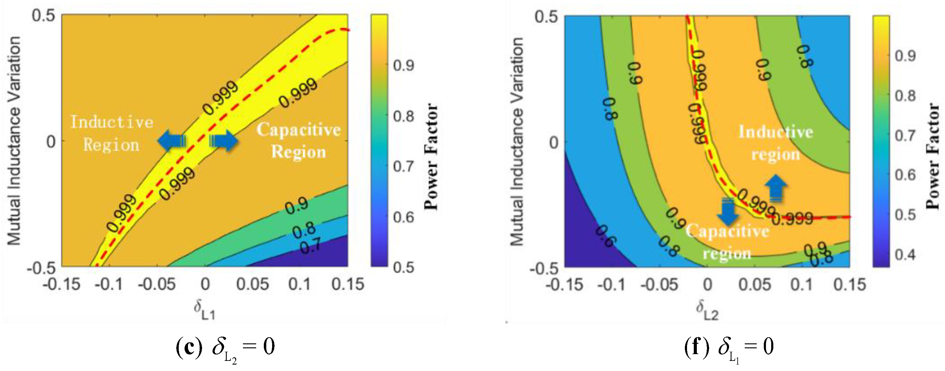
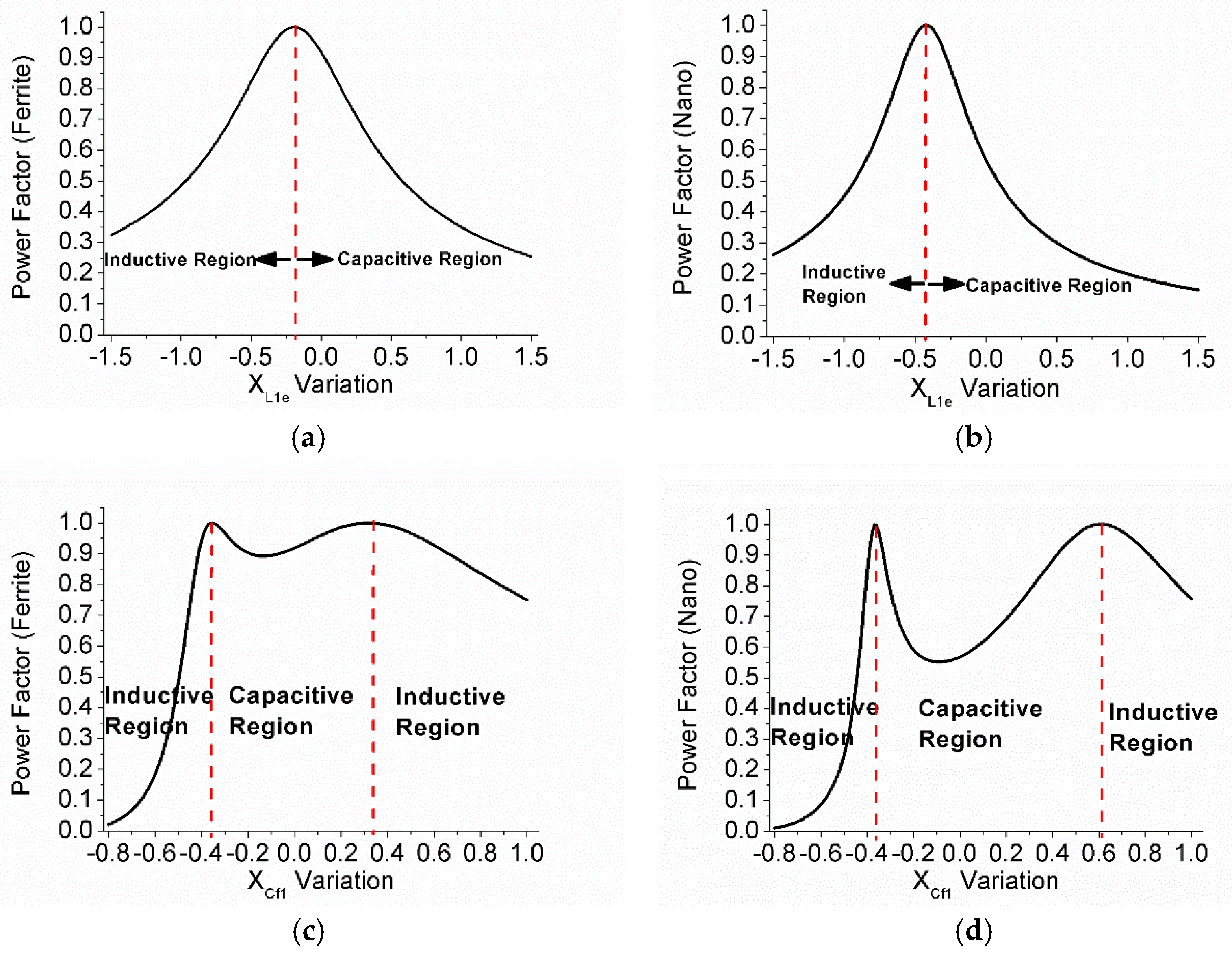
According to the above Equations (19) and (20), taking the circuit system in this paper as an example (the design parameters of which are shown in Table 2), the change in power factor on the input side of the system can be analyzed, considering coil self-inductance and mutual inductance changes of ± 15 % and ± 50 % , respectively.
When the self-inductance of the secondary coil L 2 is δ L 2 = 0.15 (shown in Figure 3a) and the mutual inductance increases, the system changes to become inductive, and with an enhancement in the mutual inductance, the influence of this mutual inductance on the system’s properties gradually becomes less than that of the primary coil’s self-inductance. When the system enters the capacitive interval, the power factor clearly decreases with the change in δ L 1 . When the mutual inductance of the system is reduced, the system becomes capacitive, but the mutual inductance maintains a significant influence on the power factor of the system. When δ L 2 = 0.15 (shown in Figure 3b), the whole system resides in the capacitive interval, and when the mutual inductance is ± 50 % , it does not affect the capacitive properties of the system. Therefore, when designing the resonant parameters of the coil and the system, the self-inductance of the secondary coil should not be allowed to fall into this range; however, the system still becomes increasingly capacitive with increases in the mutual inductance, and with an increase in δ L 1 , the power factor clearly decreases. When δ L 2 = 0 (as shown in Figure 3c) and the mutual inductance of the system increases, the system enters the inductive region. When the mutual inductance is reduced, the system becomes capacitive, and with increases in the self-inductance of the primary coil, the system becomes more capacitive.
In summary, when the δ L 2 is constant, the increase in mutual inductance enables the system to work in the inductive range, and a reduction in the self-inductance L 1 of the primary coil will lead to a reduction in the power factor of the system, which will cause it to operate in the capacitive range.
When the change in the self-inductance of the primary coil L 1 is δ L 1 = 0.15 (shown in Figure 3d) and the mutual inductance is increasing, the influence of the change in secondary self-inductance on the properties of the system is greater than that of the mutual inductance. At this time, with the increase in its secondary self-inductance, the system tends to become inductive, and when the secondary self-inductance decreases, the system tends to become capacitive, with no apparent change in mutual inductance. When the system’s mutual inductance decreases, its influence gradually becomes dominant, and the secondary self-inductance decreases gradually. When the mutual inductance increases, the system tends to become inductive, and when the mutual inductance decreases, the system tends to become capacitive, with the influence of secondary self-inductance being relatively very small. When δ L 1 = 0 (shown in Figure 3f), it shows the same change trend as Figure 3d. When δ L 1 = 0.15 (shown in Figure 3e), the mutual inductance does not affect the properties of the system when it is within the ± 50 % interval. At this time, the nature of the system tends to become sensitive to an increase in the secondary coil’s self-inductance, while it tends to become capacitive when the secondary coil’s self-inductance decreases.
In conclusion, when the mutual inductance of the system increases, the equivalent input impedance of the detuned LCC/SP topology shifts into the inductive interval, but the degree of change will be affected by the change in the self-inductance of the secondary coil. When the self-inductance of the secondary coil begins to decrease, the influence of the mutual inductance will be weakened, and the self-inductance of the secondary coil will come to occupy the dominant. When the self-inductance of the secondary coil begins to increase, the influence of mutual inductance will gradually increase, and the effect of the change in the self-inductance of the primary coil will be almost the same as that of mutual inductance. When the inductance of the primary coil increases, the system becomes capacitive, while when the primary coil enters a decreasing state, the system becomes inductive. According to a comparison between Figure 3c,f, when the mutual inductance of the system is low, it is more likely to fall into the capacitive range, resulting in the induction of poor working conditions for the switch tube. When the mutual inductance is near the desired value or higher, a change in the self-inductance L 2 of the secondary coil will more readily affect the power factor of the system, causing the system to fall into the capacitive range. This suggests that in terms of coil design, in order to ensure dislocation, a change in the secondary’s coil self-inductance will be more effective; the primary design will be more accessible, but the secondary design requirements will be more stringent.
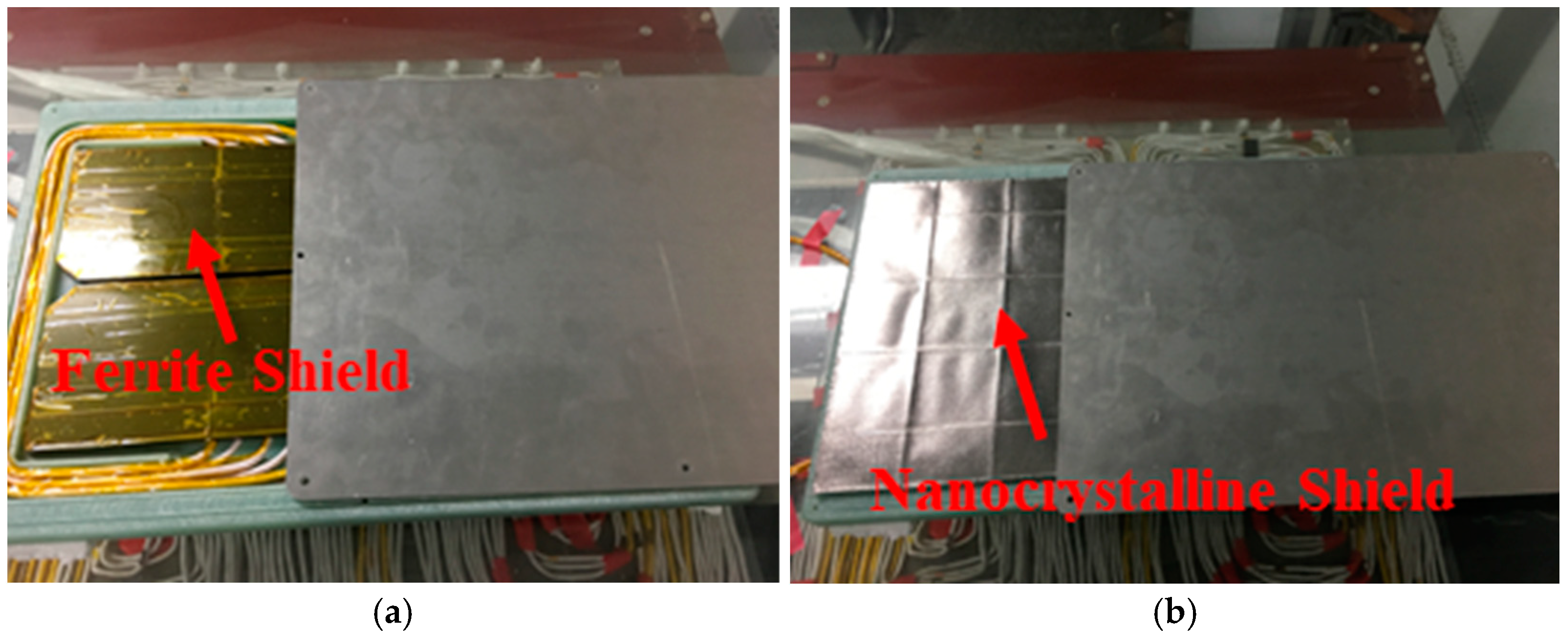
According to our analysis of the LCC/SP detuning circuit model, changes in the self-inductance and mutual inductance of the coil will have a significant impact on the power factor of the system, so it is considered necessary to introduce variable resonant matching components to ensure that the system will still work in the high power factor range during dislocation or when magnetic shielding materials are present.

3. Self-Tuning LCC/SP System Analysis and the Control Scheme

3.1. The Working Principle of the SCC

Using novel PWM SCC technology, the capacitance of the capacitor can be changed via PWM modulation. Then, the system can continue to work in the high power factor range by adjusting the inductance/capacitance of a resonant matching component when the resonant state of the system changes. The equivalent circuit diagram of the SCC is shown in Figure 4.
Here, C 0 is the thin film capacitor and M 1 and M 2   are two MOSFETs, which are connected in parallel at both ends of the capacitor C 0 after their connection in a reverse series. The two diodes D 3 and D 4 are connected in a reverse parallel layout at the two ends of M 1 and M 2 , respectively. Within a specific working time sequence, the external equivalent capacitance can be controlled. I i n is the input current of the entire SCC module, and the current flowing through the capacitor C 0 is I C ; the voltage across the capacitor is the same as that across the entire module, denoted as U C 0 .
The input current, control signal, and voltage at both ends of the SCC in one cycle are shown in Figure 5; the working states of the SCC are divided into six types, as shown in Figure 6. The SCC goes through eight working stages in one cycle.
In stage I, M 1 and M 2 are turned on simultaneously, and the current flow is positive. At this time, the input current flows through the switch branches M 1 and M 2 , the capacitor C 0 is short-circuited, and the voltage at both ends of the capacitor is zero.
In stage II, the M 1 is turned off, the M 2 remains turned on, and the current flow is positive. At this time, the input current flows through the capacitor C 0 , which is charged, and the voltage at both ends of the capacitor rises slowly from zero to the maximum.
In stage III, when the M 1 is turned off and the M 2 remains on, the input current is reversed, and the current flow becomes negative. A positive EMF is formed due to the storage of the capacitive charge. The input current flows preferentially through the capacitor branch, and the capacitor is discharged in reverse until the voltage at both ends becomes zero.
In stage IV, in order to preserve the ZVS and prolong the discharge time of the capacitor, the M 1 remains off, the M 2 is turned on, and the capacitor is discharged to a voltage of zero in the reverse direction, ready for reverse charging. However, due to the existence of the anti-parallel diode D 3 in switch M 1 , the reverse current will short-circuit the capacitor again through M 1 and D 3 , and so the voltage at both ends of the capacitor will remains at around zero. Here, the anti-parallel diode D 3 plays the role of current continuation and voltage clamping, which ensures the normal operation of the M 1 zero voltage switch.
In stage V, the M 1 is turned on again, while the M 2 remains on, and the current flow is negative. This stage is similar to stage I, where all the input current flows through the switch branch, the capacitor is short-circuited, and the voltage at both ends remains at zero.
In stage VI, M 1 remains on, M 2 is turned off, and the current flow is negative, which is similar to stage II. When all the input current flows through the capacitor, the C 0 is charged in reverse, and the voltage at both ends of the capacitor rises slowly from zero to the reverse maximum.
In stage VII, M 1 remains on and M 2 is turned off, which is similar to stage III; when the input current is reversed again, the current flow is positive, and the capacitor is discharged in the forward direction until the voltage at both ends is zero.
In stage VII, M 1 is kept on and M 2 is turned off, which is similar to stage VI. The current continues to flow through the anti-parallel diode D 4 , and the voltage at both ends of the capacitor is clamped, which ensures the regular operation of the M 2 zero voltage switch.
In a given period of current input, the time at which the current surpasses the zero-crossing point is defined as the start time of the period, and the delay period t = t d is defined as the beginning of the cycle to the first falling side of PMM_1. At the same time, the delay angle φ is defined as the angle of the delay time to the 2 π period, the equivalent capacitance value is C e q , and the original capacitance value is C 0 . Refer to [9] for equivalent capacitance values:
C e q = C 0 2     2 φ     sin 2 φ π

3.2. Comparison of Optimal Positions for SCCs

Based on the components present in the laboratory, the design parameters of the LCC/SP circuit with resonance parameters are shown in Table 2:
Table 2. Design value of resonance parameters.
ParametersValue
Primary compensation inductance L f 1 26.85 μH
Primary parallel compensation capacitor C f 1 135.2 nF
Primary series compensation capacitor C 1 89.9 nF
Secondary side series compensation capacitor C S 153.14 nF
Secondary side parallel compensation capacitor C P 116.4 nF
Transmitting coil self-inductance L 1 78.33 μH
Receiving coil self-inductance L 2 53.21 μH
SCC initial value C 0 49 nF
According to the analysis in the previous section, the SCC can be placed in the circuit to realize a change in the inductance/capacitance of a resonant component. If the SCC is placed on the secondary side, it is necessary to increase the communication module in order to realize pure resistance in the input impedance of the system, which will increase the complexity and lead to stability problems in the system. Thus, the SCC is placed on the primary side, where there are three resonant components, the series compensation capacitor C 1 , the parallel compensation capacitor C f 1 and the series compensation inductor L f 1 . The impact of placement in three different locations needs to be considered.
The influence of placing SCCs in different positions is evaluated via two aspects: the sensitivity of the power factor to changes in the capacitance/inductance of resonant components, and the influence of change in the inductance/capacitance of different components on the harmonic characteristics of the system.
Firstly, the influence of changes in the inductance/capacitance of different components on the harmonic characteristics of the system was evaluated, and the Fourier decomposition method was used to decompose the current of the primary coil, considering that the secondary coil is made of ferrite and a nanocrystalline material. It is obvious that when the SCC is connected in series with the series inductor I L f 1 , the fundamental amplitude of I L f 1 will be the highest (15.68 when the secondary side’s magnetic shielding material is ferrite and 19.73 when the nanocrystalline material is used). At this time, the current waveform is more sinusoidal, and has the most negligible influence on the system. However, when the SCC is connected in series with the series compensation capacitor C 1 , the amplitude of the fundamental wave decreases, and the harmonic effect increases (13.14 when the second side’s magnetic shielding is ferrite and 9.45 when it is nanocrystalline). At this point, the current waveform begins to worsen, and the amplitude of the fundamental component will be lowest when the SCC is connected in series with the parallel compensation capacitor C f 1 (9.77 when the secondary side’s magnetic shielding is ferrite and 6.69 when it is nanocrystalline).
For a closed-loop system, it is necessary to determine the phase of the primary coil current I L f 1 and the inverter output voltage phase u A B . Thus, zero-crossing detection is adopted, and the phase difference is determined by observing the zero-crossing point of each increase in the current and voltage phases. If I L f 1 is seriously distorted, as shown in Figure 7f, there will be more than two zero-crossing points in one cycle, which will lead to a malfunction in the SCC. Given the influence on the harmonic characteristics of the system, the SCC and the series inductor L f 1 should be connected in series.
Considering the sensitivity of the power factor to the capacitance/inductance of different resonant components, Figure 8 shows the two maximum dislocation points of Fe (100, 75, 130) and Nano (100, 75, 110), the possible coil magnetic shielding materials that can be used in the secondary sides. Power factor change curves are presented when each resonance parameter ( X L 1 e , X C f 1 , X L f 1 ) fluctuates. The equivalent primary impedance value during resonance is defined as the equivalent primary impedance value X L 1 e ( X L 1 e _ r e f is the nominal value defined in Table 1). As shown in Equation (22), the impedance value of the equivalent primary parallel compensation capacitor under resonance is X C f 1 ( X C f 1 _ r e f is the nominal value), and X L f 1 is the equivalent primary series compensation inductance impedance value. The relative change rates X L 1 e   Variation , X C f 1   Variation , and X L f 1   Variation can be defined as:
X L 1 e = ω 0 ( L 1 1 ω 0 2 C 1 ) X L 1 e   Variation = X L 1 e X L 1 e _ r e f X L 1 e _ r e f X C f 1   Variation = X C f 1 X C f 1 _ r e f X C f 1 _ r e f X L f 1   Variation = X L f 1 X L f 1 _ r e f X L f 1 _ r e f
As regards the actual physical meaning of the SCC, the range is adjustable. The parallel compensation capacitor is 0 when X C f 1   Variation     1 and Cf1 is infinite, and these conditions cannot be realized by the SCC. When X L 1 e   Variation 0 , an additional inductor must be added. Similarly, additional inductors need to be introduced when X L f 1   Variation 0 . Economically speaking, the cost of the device will be relatively low when the SCC is placed in Cf1.
Figure 8 illustrates the sensitivity analysis of SCC regulation, in which the SCC was placed in different resonant elements. When the SCC was placed in the C 1 position, it changed rapidly near the point of resonance, and the sensitivity was very high. In practical applications, the capacitance of the SCC may fluctuate. If the SCC is placed in the C 1 position, a slight fluctuation in X L 1 e will cause a significant change in the power factor, especially under the working condition of nano (100, 75, 110). When the SCC was placed in the C f 1 position, two relatively close resonant points could be identified, resulting in instability in the SCC controller. When the SCC was placed in the L f 1 position, the rate of change in the power factor was relatively low. With Fe (100, 75, 130), the X L f 1 is less sensitive to the power factor of the system and is more easily stabilized at the point of resonance.

3.3. Self-Tuning LCC/SP System Control Method

According to the above analysis, the SCC is set at the position of the series resonant inductor L f 1 to introduce regulated variation Δ L L f 1 in the series compensation inductor L f 1 . Here, L f 1 and L f 2 represent the actual inductance value before and after adjustment, respectively, and δ L f 1 is the relative change value of L f 1 .
Δ L f 1 = L f 1 L f 1 δ L f 1 = Δ L f 1 L f 1
The normalized impedance Z i n c of the emitter after the inductance adjustment is introduced can be obtained as follows:
Z i n c = ( ω n 2 λ M 2 ( δ M   +   1 ) 2 Z s n + j ω n ( 1 + δ L 1 ) + ( 1 λ L f 1 λ M 2 λ L 2 e λ ) j ω n ) λ L f 1 j ω n ω n 2 λ M 2 ( δ M + 1 ) 2 Z s n + j ω n ( 1 + δ L 1 ) + ( 1 λ L f 1 λ M 2 λ L 2 e λ ) j ω n + λ L f 1 j ω n + j ω n λ L f 1 ( 1 + δ L f 1 )
In order to avoid the problem of system instability due to frequency conversion, the system is subjected to fixed frequency control and made to work at the resonant frequency. ω n = 1 is substituted, and the following can be obtained:
Z i n _ ω 0 c = ( λ M 2 ( δ M + 1 ) 2 Z s n + j ( 1 + δ L 1 ) + ( 1 λ L f 1 λ M 2 λ L 2 e λ ) j ) λ L f 1 j λ M 2 ( δ M + 1 ) 2 Z s n + j ( 1 + δ L 1 ) + ( 1 λ L f 1 λ M 2 λ L 2 e λ ) j + λ L f 1 j + j λ L f 1 ( 1 + δ L f 1 )
The normalized input impedance is expressed in terms of a real part and an imaginary part.
Z i n _ ω 0 c = R i n _ ω 0 c + j X i n _ ω 0 c
As regards the equivalent input impedance, a change in the impedance value of the series compensation inductor L f 1 will only change the imaginary part of the input impedance; it will not affect the real part, so the imaginary part of the input impedance can be expressed as:
X i n _ ω 0 c = X i n _ ω 0 c + λ L f 1 δ L f 1
In order to make the imaginary part of the input impedance of the system zero when it is not resonant, and to ensure the unit power operation of the inverter output and eliminate the influence of reactive power, it is only necessary to adjust the variation in the series compensation inductor L f 1 , as follows.
δ L f 1 = X i n _ ω 0 c λ L f 1
For a set of definite systems, both X i n _ ω 0 c and λ L f 1 are fixed values. The above equation has a unique solution, and the above conditions remain satisfied when the parameters of the system are changed and stabilized. Therefore, for the system studied in this paper, we used the SCC in series with the series compensation inductor, L f 1 .
According to the previous analysis, the imaginary part of the equivalent input impedance can be offset by changing the size of the series compensation inductor L f 1 , thus eliminating the reactive power input into the system. In this case, the value of the imaginary part of the input impedance has a linear relationship with the L f 1 variation, which satisfies the monotone relationship and means that the PI method can be used for closed-loop control. The control block diagram is shown below, in which the phase angle is measured by observing the zero-crossing detection signal of the primary current i L f 1 , and an interrupt signal at t2 is generated when the rising zero-crossing point of i L f 1 is recorded. The zero-crossing detection signal of the inverter switch Q 1 is recorded at t1, which indicates the zero-crossing moment of the input square wave voltage of the inverter. The phase difference between the voltage and current of the inverter can then be obtained from (29). At the same time, the phase information of i L f 1 can also be used as a reference to determine the switching control signal of the SCC, and only one current zero-crossing detection hardware unit is required for phase difference detection and SCC adjustment. For ease of understanding, the control process is shown in Figure 9. According to Formula (29), the impedance Angle at the current sampling time can be calculated, which is compared with 25.5° (corresponding power factor is 0.9).
= 2 π ( t 1 t 2 ) T
The self-control tuning of the system can then be realized through the above design. The principle of the power factor self-tuning system is shown in Figure 10. The previous section shows that the best positioning of the SCC involves using it in series with the series compensation capacitor L f 1 . In order to achieve a broader impedance adjustment range, the value of L f 1 is expanded to twice the resonant value, i.e., 53.7   μ H .

4. Experimental Results and Discussion

4.1. Test Prototype Construction

An experimental prototype of the LCC/SP wireless charging system was built in the laboratory, in which the SCC was connected in series at the primary series compensation inductor L f 1 , as mentioned above, in order to verify the proposed control scheme.
A double D coil consists of two square coils side by side, as shown in Figure 11. After multi-objective optimization, the magnetic coupling coil group used in the prototype shown in Figure 12 was an asymmetric double D coil group [22]. The size specifications of the transmitting coil and the receiving coil used in this design are not the same, and were obtained via the multi-objective optimization of the structure of the reference coil group recommended by the SAEJ2954 standard. Maintaining a high coupling coefficient effectively controls the intensity of magnetic field leakage around the magnetic coupling coil within the prescribed range of horizontal dislocations, and the parameters of this are shown in Table 3. The coil self-inductance and mutual inductance values corresponding to other dislocations and secondary magnetic shielding materials are shown in Table 4 and Table 5. Experimental conditions refer to WPT1Z1 conditions for design (maximum power 3.7 kVA vertical spacing 100~150 mm).
As shown in Figure 13, the power supply of the system was Chroma 62100H-1000, the output capacity was between 0 and 1000 V, and the maximum output current was 10A. In order to meet the power level required for the experiment, the two sets were used in parallel. The resistance load was adopted at the load end, and the resistance value was 13.3 ohms. The power analyzer was a PW6001. In the experiment, the MOS transistors in the SCC and the inverter were both Infineon IMW120R045M1, and the diode used in the secondary side’s current doubling rectifier was Semet’s FFSH15120AOS. In order to generate the PWM signal used to control the operation of the switch tube, this design used the C2000 series DSP of Texas Instruments as the controller. The specific model was TMS320F28335. Two groups of PWM modules were used to generate the drive signal of the primary inverter, and one group was used for the drive signal of the SCC.
Two different magnetic shielding materials, nanocrystalline and ferrite, were used in this experiment, and the coils were placed on the experimental platform built in the laboratory. The test bench set the relative positions of the primary and secondary coils using infrared ranging, and these coils could be subjected to different dislocation conditions. In addition, the secondary magnetic shielding layer material could be easily replaced to assess the resulting difference in transmission performance.

4.2. Performance Analysis of the System under Different Dislocation Conditions

The experimental results obtained when the coil’s position was changed are shown in Figure 14, where the coil’s position refers to the movement of the secondary side coil relative to the primary coil under conditions of alignment, and the output voltage u A B , primary current i L f 1 , and SCC voltage u C e q of the primary inverter are recorded here. The phases of the output voltage u A B and the primary current i L f 1 of the primary inverter are very close; the system is slightly inductive, and the power factor must be above 0.9 to achieve ZVS.
For the working condition of coil position (0, 0, 110) (wherein the secondary coil is aligned with the primary coil horizontally and the distance between the vertical coils is 110 mm), the mutual inductance is higher, and an output power of 2 kW can be achieved with the input voltage of 145 V. At this time, the capacitance of the SCC is the greatest, and the power factor of the system is 0.918, which enables the operation of a high power factor.
Under different dislocation conditions, with reductions in the mutual inductance, the system will reorientate in the capacitive direction, and the imaginary part of the input impedance will change. Therefore, the SCC (Equation (21)) should also be reduced accordingly. The corresponding delay angle φ also increases gradually, and the equivalent voltages at either end of the SCC decrease gradually; however, the system will maintain high power factor operation.
Subsequently, the ZVS state of the SCC can be achieved under the working condition of (0, 0, 110). As shown in Figure 15a, the waveform of the voltage U D S at both ends of the SCC’s MOS transistor and the gate control signal U G S are displayed. The MOSFET turns on after the voltage of the drain–source poles reaches zero, which will be amplified, as shown in Figure 15b. We can thus confirm that the SCC will be in the ZVS state during the system’s operation.
Considering that the test bench can be used to analyze the transmission performance of different coil or magnetic shielding materials, the resonant matching circuit should facilitate the self-adjustment of the power factor via the magnetic shielding material’s structure in order to ensure the system’s efficient operation. Therefore, in this paper, two different magnetic shielding materials, ferrite and nanocrystalline, have been used to verify the power factor adjustment ability of the self-regulating system. After replacing the material of the magnetic shielding layer of the coil with nanocrystalline, the self-inductance value of the secondary side and the mutual inductance value of the coil will be changed considerably. Between the (0, 0, 110) @Fe condition and the (100, 75, 110) @Nano condition, the mutual inductance value changed by 47.7% (from 19.12 uH to 10 uH), and the secondary side’s self-inductance value changed by 10% (from 54.10 uH to 48.5 uH).

4.3. System Closed-Loop Performance Verification

We define the system’s input impedance angle as the phase difference between voltage u a b and current i L f 1 . DC efficiency is the ratio between P 1 and P 3 , as shown in Figure 16. When the voltage phase is ahead of the current phase, the impedance angle is positive, and the system is inductive. The impedance angle is negative and the system is capacitive when the voltage phase lags behind the current phase. Figure 17a,b show the relationship between the system input impedance angle, the DC efficiency, and the use of different magnetic shielding layer materials and dislocations. Figure 17c,d show the relationship between power loss and efficiency in the inverter with different magnetic shielding materials and dislocations (inverter efficiency is defined as the ratio of P 1 to P 2 , as shown in Figure 16), while Figure 17e,f show the relationship between the input voltage related to a 2 kW output power and different magnetic shielding materials and dislocations.
According to Figure 17, it does not matter whether the secondary magnetic shielding layer material is nanocrystalline or ferrite. When using an SCC, the impedance angle will be positive and the system will be weakly inductive, which is conducive to the inverter achieving ZVS in a better working state and the power factor being more than 0.9, which is high power factor operation. It is worth noting that with greater dislocation, the total impedance of the system will increase. At the same output power, the input current I d c will decrease, and the current on the corresponding branches will also decrease such that the current loss on the line decreases accordingly. Therefore, when SCC tuning is added to ensure that the inverter will always work in ZVS (as shown in Figure 17a,b), the efficiency of the system will increase slightly with the increase in dislocation. When the secondary magnetic shielding material is ferrite and the dislocation is altered from (50, 50, 130) to (100, 75, 130), the efficiency will increase when SCC tuning is employed, but it will decrease when it is not. Furthermore, in Figure 17c, we see that the efficiency of the inverter is as low as 94%, and the loss of the inverter is 124 W, which are the dominant factors leading to the reduction in transmission efficiency due to detuning; this implies that the efficiency is reduced when SCCs are not used.
When the SCC is not used for automatic tuning, the increase in dislocations will cause the system to gradually become capacitive (when the secondary magnetic shielding layer material is nanocrystalline, and in the case of (50, 50, 130) @Fe). Under these circumstances, the inverter cannot work in the ZVS state, which has a tremendous negative impact on the life of the components. Under extreme dislocation conditions, the power factor is reduced to 0.68 with (100, 75, 130) @Fe, and to 0.61 with (100, 75, 110) @Nano, both of which are capacitive, and the working environment of the inverter is harsh. When using a SCC for self-tuning under all operating conditions, setting the inverter to work under slightly inductive conditions will be conducive to the life of the components, and the inverter loss will be shallow (the inverter efficiency is higher than 98%). Combined with Figure 17e,f, when the output power of 2 kW is reached under the same dislocation conditions, the input voltage required for regulation of the SCC will be relatively low, the voltage stress on the DC bus capacitor C d c l i n k will be relatively small, and the life of the components can be prolonged.
Figure 18a shows the transition period of SCC tuning under the conditions of (100, 75, 130) @Fe when the input voltage U dc of the DC source is 204 V. Obviously, the output power increases from 1508 W to 1995 W in 3 m S , and the power factor increases from 0.68 to 0.91. Figure 18b shows the inverter voltage u A B and current waveform   i L f 1 before tuning. Figure 18c shows the inverter voltage u A B and current waveform i L f 1 after tuning, indicating that the system changes from capacitive to weakly inductive when the input voltage remains unchanged and the output power increases from 1.2 kW to 2 kW.

5. Conclusions

In this study, a self-tuning LCC/SP WPT system was introduced. When using a SCC, the WPT system always exhibits a high power factor, which allows it to adapt to the changes taking in places in the coils under conditions of different degrees of dislocations or different magnetic shielding materials. The non-resonant circuit model of LCC/SP compensation was deduced by normalization, the influence of changes in self-inductance/mutual inductance on the power factor was deduced, and it was clarified that the power factor, as well as the change and relative change value δ L f 1 , of the primary series’ resonant inductance L f 1 have a linear functional relationship. The self-tuning of the power factor was realized using SCC through the PI control method. In addition, a 2-kW output power platform was built to verify that this system can always run with a high power factor under conditions of 47.7% mutual inductance and 10% secondary self-inductance variations, which significantly reduce the losses of the inverter and improve its efficiency. This method can be applied to the wireless power transmission test bench to test the transmission performance of many new types of magnetic shielding materials without changing the circuit parameters. The LCC-SP output power self-tuning system can be achieved by adjusting another passive component in the compensation circuit and working synergistically with the power factor self-tuning method proposed in this paper. This will be the authors’ future research topic.

Author Contributions

Conceptualization, Z.L. and M.X.; methodology, Y.Z.; software, Y.Z.; validation, Y.Z. and Z.L.; formal analysis, Y.Z.; investigation, X.W.; resources, H.D.; data curation, Y.Z.; writing—original draft preparation, Y.Z.; writing—review and editing, Z.L.; visualization, Y.Z.; supervision, X.W.; project administration, H.D.; funding acquisition, X.W. All authors have read and agreed to the published version of the manuscript.

Funding

This research received no external funding.

Institutional Review Board Statement

Not applicable.

Informed Consent Statement

Not applicable.

Data Availability Statement

Not applicable.

Conflicts of Interest

The authors declare no conflict of interest.

Nomenclatures

SymbolExplanation
M mutual inductance between the two coils
C e q the equivalent capacitance value of SCC
C 0 thin film capacitors for SCC
L f 1 series compensation inductor of the primary side.
C 1 series compensation capacitor of the primary side.
C P parallel compensation capacitor of the secondary side.
u A B sine-wave output voltage of the secondary side before rectifier
L 1 e equivalent inductance of the primary side after partial compensation.
ω operating frequency of the system
Z S _ r e f the transmitter input impedance of a system operating at a resonant frequency
Z i n the input impedance
R i n the real part of input impedance at the receiving end of the system
α active power coefficient
P F power factor
L 2 the actual value of L 2 after changing the resonance parameters of the system
Δ L 1 the difference between L 1 and L 1
Δ M the difference between M and M
δ M the ratio of the mutual inductance change to the initial value
Z 0 the equivalent impedance mode of the transmitting coil
λ the ratio of the self-inductance of the secondary side to the primary coil
λ L 2 e the ratio of the secondary side’s equivalent series compensation inductance to the self-inductance of the same side coil
Z s n the equivalent normalized receiver impedance
R i n n the real part of the normalized input impedance (which takes into account the variation in coil parameters)
P F n n equivalent normalized power factor (which takes into account the variation in coil parameters)
X L 1 e _ r e f nominal equivalent impedance of primary coil
X C f 1 _ r e f nominal impedance of primary side shunt compensation capacitor
X L f 1 _ r e f nominal impedance value of compensating inductance in series of primary side
X L 1 e   Variation the relative change rates of X L 1 e
X L f 1   Variation the relative change rates of X L f 1
Δ L L f 1 the difference between L f 1 and L f 1
Z i n _ ω 0 c normalized transmitter variable impedance operating at resonant frequency
X i n _ ω 0 c the imaginary part of the normalized transmitter variable impedance operating at resonant frequency
phase difference between inverter voltage and current
U i n system input DC voltage.
L 1 self-inductance of the primary coil.
L 2 self-inductance of the secondary coil.
C f 1 parallel compensation capacitor of the primary side.
C S series compensation capacitor of the secondary side.
U A B phasor of the input voltage u A B
R E simplified equivalent output resistance
L 2 e equivalent inductance of the secondary side after partial compensation
ω 0 the resonant operating frequency of the system
Z i n _ r e f input impedance of the system operating at resonant frequency
Z S transmitter input impedance
X i n the imaginary part of input impedance at the receiving end of the system
β reactive power coefficient
L 1 the actual value of L 1 after changing the resonance parameters of the system
M the actual value of M after changing the resonance parameters of the system
Δ L 2 the difference between L 2 and L 2
δ L 1 , δ L 2 between the self-inductance change and the initial value
ω n the ratio of the operating frequency to the resonant frequency
R n the ratio of the equivalent impedance mode of the transmitting coil to the equivalent load resistance
λ L f 1 the ratio of the primary series’ compensation inductance to the self-inductance of the same side coil
λ M the ratio of the self-inductance of the primary coil
Z i n n the equivalent normalized emitter impedance
X i n n the imaginary part of the normalized input impedance (which takes into account the variation in coil parameters)
Z i n c Normalized transmitter adjustable impedance
X L 1 e equivalent impedance of primary coil
X C f 1 impedance of primary side shunt compensation capacitor
X L f 1 impedance value of compensating inductance in series of primary side
X C f 1   Variation the relative change rates of X C f 1
L f 1 after adjusting the actual value of the primary side series compensation inductance
δ L f 1 the relative change value of L f 1
R i n _ ω 0 c the real part of the normalized transmitter variable impedance operating at resonant frequency
T System cycle

References

  1. Luo, Z.; Nie, S.; Pathmanathan, M.; Han, W.; Lehn, P.W. 3-D Analytical Model of Bipolar Coils with Multiple Finite Magnetic Shields for Wireless Electric Vehicle Charging Systems. IEEE Trans. Ind. Electron. 2022, 69, 8231–8242. [Google Scholar] [CrossRef]
  2. Lu, C.; Huang, X.; Liu, X.; Zeng, Y.; Liu, R.; Rong, C.; Liu, M. Design and Optimization of the Low-Frequency Metasurface Shield for Wireless Power Transfer System. IEEE Trans. Transp. Electrif. 2022, 8, 723–733. [Google Scholar] [CrossRef]
  3. Mi, C.C.; Buja, G.; Choi, S.Y.; Rim, C.T. Modern Advances in Wireless Power Transfer Systems for Roadway Powered Electric Vehicles. IEEE Trans. Ind. Electron. 2016, 63, 6533–6545. [Google Scholar] [CrossRef]
  4. Shevchenko, V.; Husev, O.; Strzelecki, R.; Pakhaliuk, B.; Poliakov, N.; Strzelecka, N. Compensation Topologies in IPT Systems: Standards, Requirements, Classification, Analysis, Comparison and Application. IEEE Access 2019, 7, 120559–120580. [Google Scholar] [CrossRef]
  5. Wu, X.; Zhang, W.; Xia, C.Y.; Liu, X. Maximum Efficiency Point Tracking Control Method for Series-Series Compensated Wireless Power Transfer System. IET Power Electron. 2018, 12, 2534–2542. [Google Scholar]
  6. Kamineni, A.; Covic, G.A.; Boys, J.T. Self-Tuning Power Supply for Inductive Charging. IEEE Trans. Power Electron. 2017, 32, 3467–3479. [Google Scholar] [CrossRef]
  7. Kamineni, A.; Neath, M.J.; Covic, G.A.; Boys, J.T. A Mistuning-Tolerant and Controllable Power Supply for Roadway Wireless Power Systems. IEEE Trans. Power Electron. 2017, 32, 6689–6699. [Google Scholar] [CrossRef]
  8. Joy, E.R.; Kushwaha, B.K.; Rituraj, G.; Kumar, P. Analysis and Comparison of Four Compensation Topologies of Contactless Power Transfer System. In Proceedings of the 4th International Conference on Electric Power and Energy Conversion Systems (EPECS), Sharjah, United Arab Emirates, 24–26 November 2015. [Google Scholar]
  9. Luo, Z.; Zhao, Y.; Xiong, M.; Wei, X.; Dai, H. A Self-Tuning LCC/LCC System Based on Switch-Controlled Capacitors for Constant-Power Wireless Electric Vehicle Charging. IEEE Trans. Ind. Electron. 2022. [Google Scholar] [CrossRef]
  10. Li, W.; Wei, G.; Cui, C.; Zhang, X.; Zhang, Q. A Double-Side Self-Tuning LCC/S System Using a Variable Switched Capacitor Based on Parameter Recognition. IEEE Trans. Ind. Electron. 2021, 68, 3069–3078. [Google Scholar] [CrossRef]
  11. Gu, Y.; Wang, J.; Liang, Z.; Zhang, Z. Mutual-Inductance-Dynamic-Predicted Constant Current Control of LCC-P Compensation Network for Drone Wireless In-Flight Charging. IEEE Trans. Ind. Electron. 2022. [Google Scholar] [CrossRef]
  12. Mostafa, A.; Wang, Y.; Zhang, H.; Lu, F. A Z-Class LCC-P Compensated IPT System with a Reverse Coupled Compensation Inductor. In Proceedings of the 2021 IEEE PELS Workshop on Emerging Technologies: Wireless Power Transfer (WoW), San Diego, CA, USA, 1–4 June 2021; pp. 1–5. [Google Scholar]
  13. Chen, Y.; Zhang, H.; Shin, C.S.; Seo, K.H.; Kim, D.H. A Comparative Study of S-S and LCC-S Compensation Topology of Inductive Power Transfer Systems for EV Chargers. In Proceedings of the 2019 IEEE 10th International Symposium on Power Electronics for Distributed Generation Systems (PEDG), Xi’an, China, 3–6 June 2019. [Google Scholar]
  14. Zhang, Y.; Yan, Z.; Liang, Z.; Li, S.; Mi, C.C. A High-Power Wireless Charging System Using LCL-N Topology to Achieve a Compact and Low-Cost Receiver. IEEE Trans. Power Electron. 2019, 35, 131–137. [Google Scholar] [CrossRef]
  15. Xiong, M.; Dai, H.; Li, Q.; Jiang, Z.; Luo, Z.; Wei, X. Design of the LCC-SP Topology With a Current Doubler for 11-kW Wireless Charging System of Electric Vehicles. IEEE Trans. Transp. Electrif. 2021, 7, 2128–2142. [Google Scholar] [CrossRef]
  16. Yang, J.; Zhang, X.; Zhang, K.; Cui, X.; Yang, X. An LCC-SP Compensated Inductive Power Transfer System and Design Considerations for Enhancing Misalignment Tolerance. IEEE Access 2020, 8, 193285–193296. [Google Scholar] [CrossRef]
  17. Zhang, X.; Cai, T.; Duan, S.; Feng, H.; Hu, H.; Niu, J.; Chen, C. A Control Strategy for Efficiency Optimization and Wide ZVS Operation Range in Bidirectional Inductive Power Transfer System. IEEE Trans. Ind. Electron. 2019, 66, 5958–5969. [Google Scholar] [CrossRef]
  18. Li, S.; Li, W.; Deng, J.; Nguyen, T.D.; Mi, C.C. A Double-Sided LCC Compensation Network and Its Tuning Method for Wireless Power Transfer. IEEE Trans. Veh. Technol. 2015, 64, 2261–2273. [Google Scholar] [CrossRef]
  19. Li, W.; Zhang, Q.; Cui, C.; Wei, G. A Self-Tuning S/S Compensation WPT System Without Parameter Recognition. IEEE Trans. Ind. Electron. 2022, 69, 6741–6750. [Google Scholar] [CrossRef]
  20. Cota, K.A.; Gray, P.A.; Pathmanathan, M.; Lehn, P.W. An Approach for Selecting Compensation Capacitances in Resonance-Based EV Wireless Power Transfer Systems With Switched Capacitors. IEEE Trans. Transp. Electrif. 2019, 5, 1004–1014. [Google Scholar] [CrossRef]
  21. Hu, H.; Cai, T.; Duan, S.; Zhang, X.; Niu, J.; Feng, H. An Optimal Variable Frequency Phase Shift Control Strategy for ZVS Operation Within Wide Power Range in IPT Systems. IEEE Trans. Power Electron. 2020, 35, 5517–5530. [Google Scholar] [CrossRef]
  22. Luo, Z.; Wei, X.; Pearce, M.; Covic, G.A. Multi-objective Optimization of Inductive Power Transfer Double-D Pads for Electric Vehicles. IEEE Trans. Power Electron. 2020, 36, 5135–5146. [Google Scholar] [CrossRef]
Figure 1. LCC/SP topology.
Energies 15 03980 g001
Figure 2. Simplified LCC/SP topology.
Energies 15 03980 g002
Figure 3. The effect of coil parameter changes on the system’s power factor. (a) When the secondary side’s self-inductance value increases by 15%; (b) when the secondary side’s self-inductance value decreases by 15%; (c) when the secondary side’s self-inductance value remains unchanged; (d) when the primary side’s self-inductance value increases by 15%; (e) when the primary side’s self-inductance value decreases by 15%; and (f) when the secondary side’s self-inductance value remains unchanged.
Energies 15 03980 g003aEnergies 15 03980 g003b
Figure 4. Equivalent circuit diagram of SCC.
Energies 15 03980 g004
Figure 5. SCC control logic in one cycle.
Energies 15 03980 g005
Figure 6. Six working states of the SCCs.
Energies 15 03980 g006
Figure 7. The influence on the harmonic characteristics of the system when the inductance value/capacitance value of different components changes. (a) The effect of series compensation inductance @Fe; (b) the effect of series compensation inductance @Nano; (c) the effect of parallel compensation capacitor @Fe; (d) the effect of parallel compensation capacitor @Nano; (e) the effect of series compensation capacitor @Fe; and (f) the series compensation capacitance effect @Nano.
Energies 15 03980 g007
Figure 8. Power factor sensitivity analysis. (a) The equivalent inductance value of the primary side’s effects @Fe; (b) the equivalent inductance value of the primary side’s effects @Nano; (c) the value of the parallel compensation capacitor’s effects @Fe; (d) the parallel compensation capacitor value’s effects @Nano; (e) the series compensation inductance value’s effects @Fe; and (f) the series compensation inductance value’s effects @Nano.
Energies 15 03980 g008aEnergies 15 03980 g008b
Figure 9. System control block diagram.
Energies 15 03980 g009
Figure 10. Power factor self-tuning LCC/SP wireless charging system. 
Energies 15 03980 g010
Figure 11. Asymmetric double D coil set where (a) is the receiving coil and (b) is the transmitting coil.
Energies 15 03980 g011
Figure 12. (a) Ferrite core secondary pad (5 mm thick). (b) Nanocrystalline core secondary pad (4 mm thick).
Energies 15 03980 g012
Figure 13. Self-tuning LCC/SP system test prototype.
Energies 15 03980 g013
Figure 14. Tuning waveforms with different degrees of dislocation when the secondary side is a ferrite magnetic shielding material. (a) Coil position (0, 0, 110) φ = 2.168. (b) Coil position (25, 25, 120) φ   = 2.230. (c) Coil position (50, 50, 130) φ   = 2.293. (d) Coil position (100, 75, 130) φ   = 2.670.
Energies 15 03980 g014
Figure 15. SCC’s ZVS state. (a) Driving signal and drain–source voltage. (b) Enlarged diagram of driving signal and drain–source voltage.
Energies 15 03980 g015
Figure 16. Efficiency measurement.
Energies 15 03980 g016
Figure 17. Transmission performance analysis of typical LCC/SP and LCC/SP with SCC when ferrite and nanocrystalline material are used on the secondary side; (a) comparison of input impedance angle and transmission efficiency @Fe; (b) comparison of input impedance angle and transmission efficiency @Nano; (c) inverter loss vs. inverter efficiency @Fe; (d) inverter loss vs. inverter efficiency @Nano; (e) comparison of input voltage required to reach 2 kW output power @Fe; and (f) comparison of input voltage required to reach 2 kW output power @Nano.
Energies 15 03980 g017
Figure 18. Closed-loop test results. (a) Closed-loop 2 kW self-tuning experimental results; (b) inverter voltage and primary current before tuning; and (c) inverter voltage and primary current after tuning.
Energies 15 03980 g018
Table 3. Parameters of asymmetric double D magnetic coupling coil set.
ParametersValue
Equivalent   series   resistance   of   transmitting   coil   R 1 128 mΩ
The number of turns of the transmitting coil8
Transmitting size800 mm × 525 mm
Equivalent   series   resistance   of   receiving   coil     R 2 410 mΩ
Primary   and   secondary   coil   mutual   inductance     M 19.6125 μH
Receiving coil turns7
Magnetic coupling gap110 mm
Receiving coil size340 mm × 260 mm
Load   resistance   R o 13.3 Ω
Table 4. Inductance matrix with ferrite shield on receiver pad.
Secondary Pad PositionL1 (μH)L2 (μH)M (μH)
(0, 0, 100)77.85521
(25, 25, 110)77.554.518.1
(50, 50, 120)76.252.814.4
(100, 75, 130)76.253.310.8
L1, L2, and M are defined in Figure 1.
Table 5. Inductance matrix with nanocrystalline shield on receiver pad.
Secondary Pad PositionL1 (μH)L2 (μH)M (μH)
(0, 0, 100)7849.316.7
(25, 25, 100)77.849.215.9
(50, 50, 110)76.348.712.6
(100, 75, 110)76.148.510
L1, L2, and M are defined in Figure 1.
Publisher’s Note: MDPI stays neutral with regard to jurisdictional claims in published maps and institutional affiliations.

