
Benefits of Low Electron-Affinity Material as the N-Type Layer for Cu(In,Ga)S2 Solar Cell


Abstract
:1. Introduction
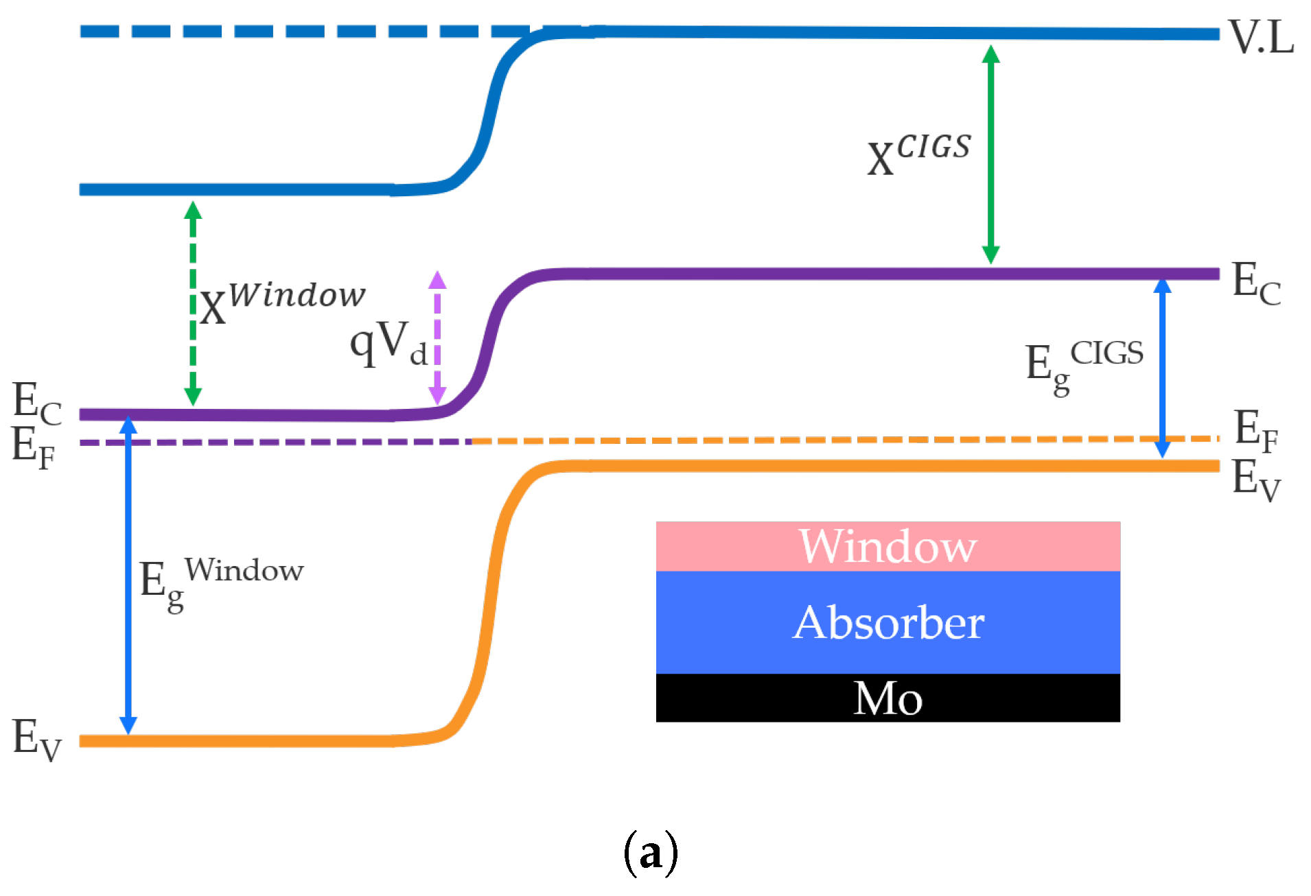
2. Theoretical- Equation
3. N-Type Layer Simulation Modelling
4. Simulation Results and Analysis
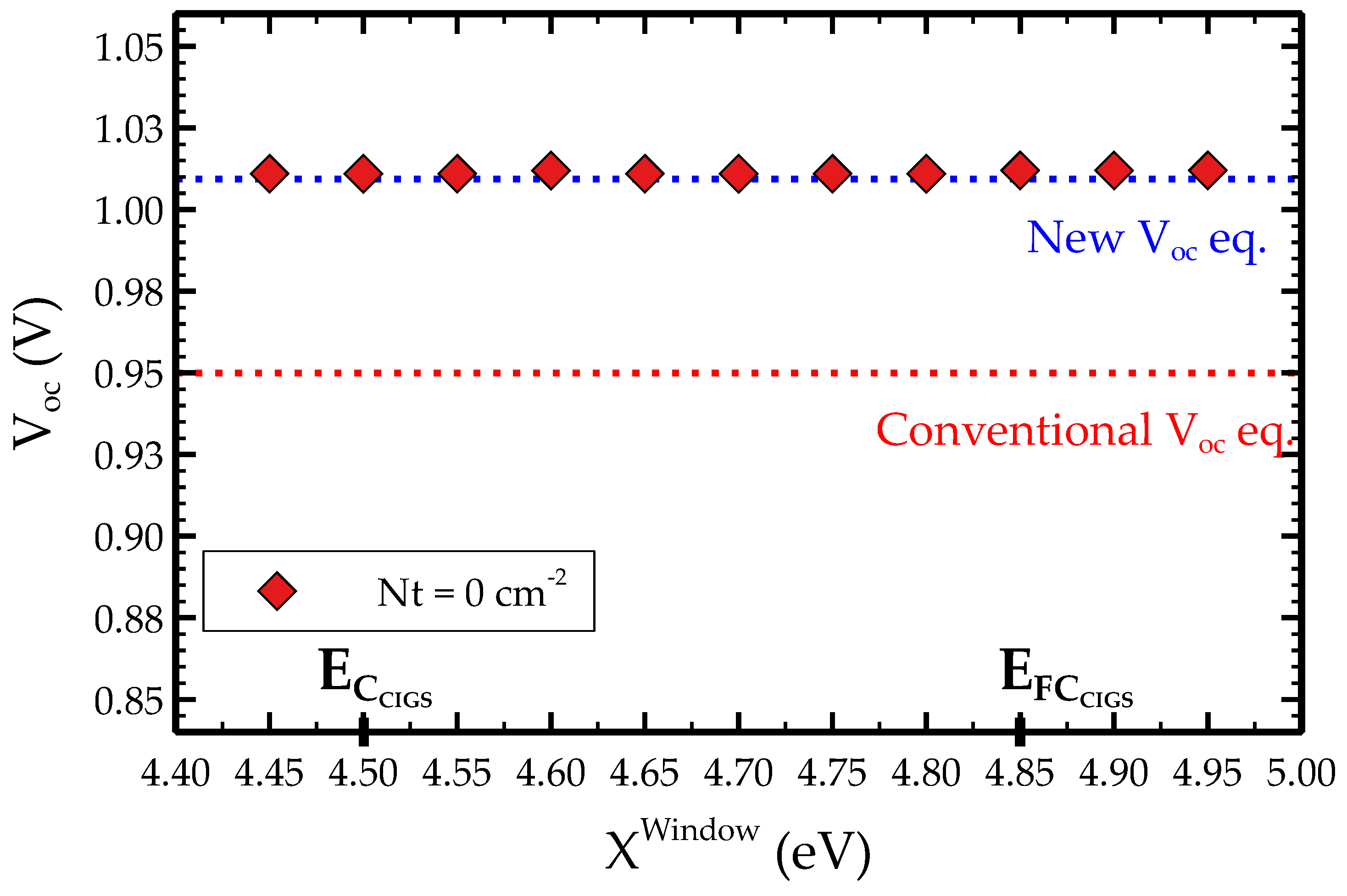
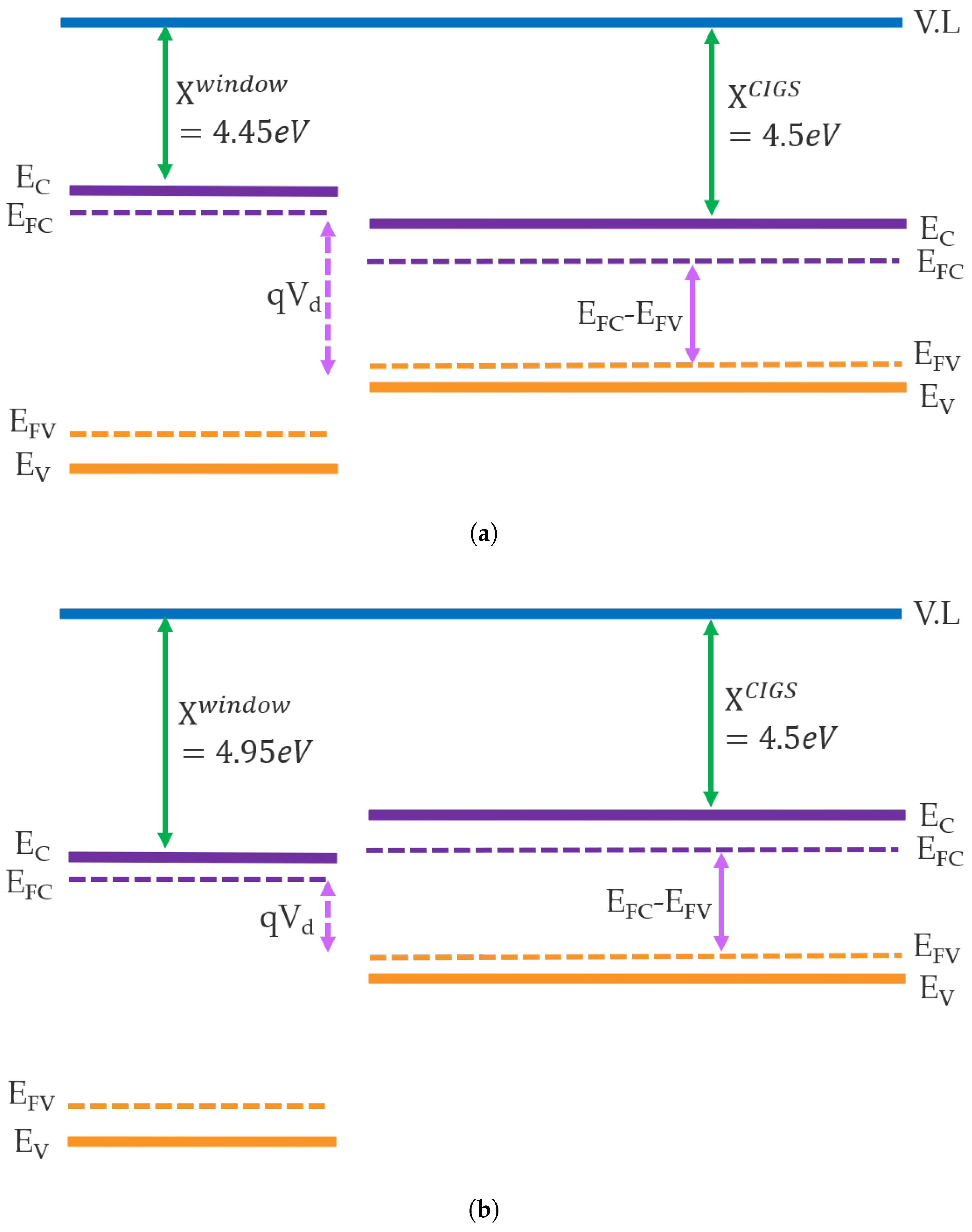
4.1. Maximum and Band Diagram Analysis in Ideal Design Condition
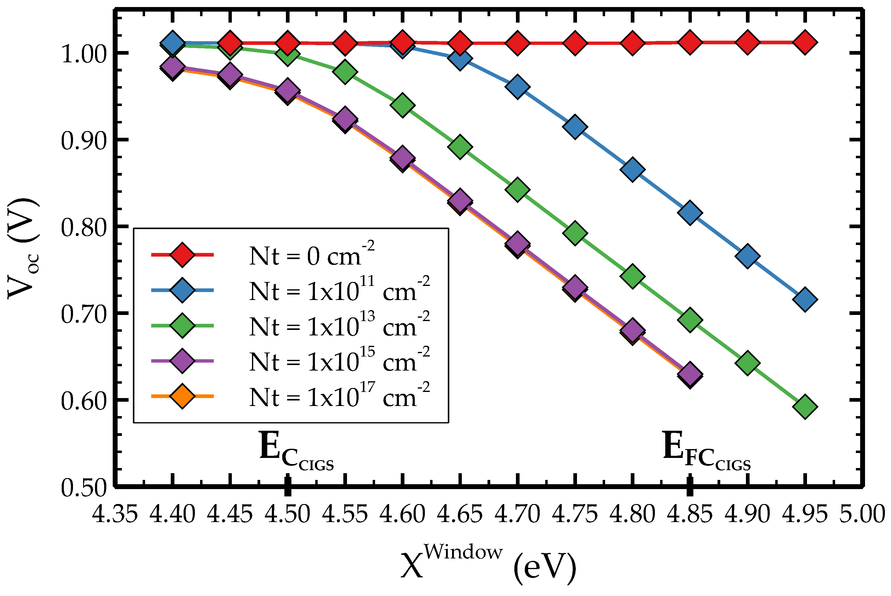
4.2. The Roles of N-Type Layer in Realistic Design Condition
4.2.1. N-Type Layer as Interface Passivation
4.2.2. N-Type Layer as Selective Electron Contact
4.3. N-Type Layer Dependence on the Ga- and S-Content in the CIG(SSe) Absorber Layer
5. Conclusions
Author Contributions
Funding
Institutional Review Board Statement
Informed Consent Statement
Data Availability Statement
Conflicts of Interest
References
- Paulson, P.; Birkmire, R.; Shafarman, W. Optical characterization of CuIn1−xGaxSe2 alloy thin films by spectroscopic ellipsometry. J. Appl. Phys. 2003, 94, 879–888. [Google Scholar] [CrossRef]
- Orgassa, K. Coherent Optical Analysis of the ZnO/CdS/Cu(In,Ga)Se2 Thin Film Solar Cell; Shaker: Baden-Württemberg, Stuttgart, 2004. [Google Scholar]
- Coutts, T.J.; Ward, J.S.; Young, D.L.; Emery, K.A.; Gessert, T.A.; Noufi, R. Critical issues in the design of polycrystalline, thin-film tandem solar cells. Prog. Photovolt. Res. Appl. 2003, 11, 359–375. [Google Scholar] [CrossRef]
- Meillaud, F.; Shah, A.; Droz, C.; Vallat-Sauvain, E.; Miazza, C. Efficiency limits for single-junction and tandem solar cells. Sol. Energy Mater. Sol. Cells 2006, 90, 2952–2959. [Google Scholar] [CrossRef] [Green Version]
- Spiess, H.W.; Haeberlen, U.; Brandt, G.; Räuber, A.; Schneider, J. Nuclear magnetic resonance in IB–III–VI2 semiconductors. Phys. Status Solidi B 1974, 62, 183–192. [Google Scholar] [CrossRef]
- Zunger, A.; Jaffe, J. Structural origin of optical bowing in semiconductor alloys. Phys. Rev. Lett. 1983, 51, 662. [Google Scholar] [CrossRef]
- Nakamura, M.; Tada, K.; Kinoshita, T.; Bessho, T.; Nishiyama, C.; Takenaka, I.; Kimoto, Y.; Higashino, Y.; Sugimoto, H.; Segawa, H. Perovskite/CIGS spectral splitting double junction solar cell with 28% power conversion efficiency. Iscience 2020, 23, 101817. [Google Scholar] [CrossRef]
- Hamtaei, S.; Brammertz, G.; Meuris, M.; Poortmans, J.; Vermang, B. Dominant Processing Factors in Two-Step Fabrication of Pure Sulfide CIGS Absorbers. Energies 2021, 14, 4737. [Google Scholar] [CrossRef]
- Rühle, S. Tabulated values of the Shockley–Queisser limit for single junction solar cells. Sol. Energy 2016, 130, 139–147. [Google Scholar] [CrossRef]
- Sze, S.; Ng, K. Physics of Semiconductor Devices; Wiley: New York, NY, USA, 2006. [Google Scholar]
- Nishimura, T.; Kasashima, S.; Hirai, Y.; Kurokawa, Y.; Yamada, A. Fabrication of Cu(In,Ga)(Se)2 solar cells with a single graded band profile. Phys. Status Solidi B 2015, 252, 1235–1238. [Google Scholar] [CrossRef]
- Hirai, Y.; Hidaka, Y.; Kurokawa, Y.; Yamada, A. Improvement of the Band Profile of Cu(In,Ga)(Se)2 Solar Cells with High-Ga Content Prepared Using a Five-Stage Method. Jpn. J. Appl. Phys. 2012, 51, 10NC03. [Google Scholar] [CrossRef]
- Hirai, Y.; Suzuki, R.; Kurokawa, Y.; Yamada, A. Numerical simulation about effects of bandgap grading in Cu(In,Ga)(Se)2 with a bandgap of 1.4 eV on solar cell performance. In Proceedings of the 2013 IEEE 39th Photovoltaic Specialists Conference (PVSC), Tampa, FL, USA, 16–21 June 2013; pp. 3307–3309. [Google Scholar]
- Chung, C.H. Method to Determine the Recombination Characteristics of Minority Carriers in Graded-Band-Gap Solar Cells. Phys. Rev. Appl. 2019, 12, 24060. [Google Scholar] [CrossRef]
- Za’abar, F.; Zuhdi, A.W.M.; Bahrudin, M.S.; Abdullah, S.F.; Hasani, A.H. Numerical modelling of graded bandgap CIGS solar cell for performance improvement. In Proceedings of the 2019 Electron Devices Technology and Manufacturing Conference (EDTM), Singapore, 12–15 March 2019; pp. 469–471. [Google Scholar]
- Sadono, A.; Hino, M.; Nakada, K.; Yamada, A. Effect of an additional Cu-deficient layer deposition on alkali treated Cu(In,Ga)(Se)2 solar cells deposited at low temperature. Sol. Energy Mater. Sol. Cells 2018, 184, 67–72. [Google Scholar] [CrossRef]
- Sadono, A.; Ogihara, T.; Hino, M.; Yamamoto, K.; Yamada, A. Peeled-off flexible Cu(In,Ga)(Se)2 solar cells and Na diffusion effects on cell performances. Electron. Mater. Lett. 2016, 12, 494–498. [Google Scholar] [CrossRef]
- Nishimura, T.; Toki, S.; Sugiura, H.; Nakada, K.; Yamada, A. Effect of Cu-deficient layer formation in Cu(In,Ga)Se2 solar-cell performance. Prog. Photovolt. Res. Appl. 2018, 26, 291–302. [Google Scholar] [CrossRef]
- Ogihara, T.; Sadono, A.; Nishimura, T.; Nakada, K.; Yamada, A. Control of valence band offset of Cu(In,Ga)Se2 solar cells with single-graded band profile. Jpn. J. Appl. Phys. 2017, 56, 062301. [Google Scholar] [CrossRef]
- Ji, S.; Hayakawa, T.; Suyama, N.; Nakada, K.; Yamada, A. Enhancement of Cu(In,Ga)(Se)2 solar cells efficiency by controlling the formation of Cu-deficient layer. Jpn. J. Appl. Phys. 2020, 59, 041003. [Google Scholar] [CrossRef]
- Wang, Y.; Muryobayashi, T.; Nakada, K.; Li, Z.; Yamada, A. Correlation between carrier recombination and valence band offset effect of graded Cu(In,Ga)Se2 solar cells. Sol. Energy Mater. Sol. Cells 2019, 201, 110070. [Google Scholar] [CrossRef]
- Nakamura, M.; Yamaguchi, K.; Kimoto, Y.; Yasaki, Y.; Kato, T.; Sugimoto, H. Cd-free Cu(In,Ga)(S,Se)2 thin-film solar cell with record efficiency of 23.35%. IEEE J. Photovolt. 2019, 9, 1863–1867. [Google Scholar] [CrossRef]
- Sugimoto, H.; Hiroi, H.; Iwata, Y.; Yamada, A. Recent progress in high efficiency pure sulfide CIGS solar cells. In Proceedings of the 27th International Photovoltaic Science and Engineering Conference, Kyoto, Japan, 12–17 November 2017. [Google Scholar]
- Gloeckler, M.; Sites, J. Efficiency limitations for wide-band-gap chalcopyrite solar cells. Thin Solid Film 2005, 480, 241–245. [Google Scholar] [CrossRef]
- Wei, S.H.; Zunger, A. Calculated natural band offsets of all II–VI and III–V semiconductors: Chemical trends and the role of cation d orbitals. Appl. Phys. Lett. 1998, 72, 2011–2013. [Google Scholar] [CrossRef] [Green Version]
- Larsson, F.; Nilsson, N.S.; Keller, J.; Frisk, C.; Kosyak, V.; Edoff, M.; Törndahl, T. Record 1.0 V open-circuit voltage in wide band gap chalcopyrite solar cells. Prog. Photovolt. Res. Appl. 2017, 25, 755–763. [Google Scholar] [CrossRef] [Green Version]
- Hiroi, H.; Iwata, Y.; Adachi, S.; Sugimoto, H.; Yamada, A. New world-record efficiency for pure-sulfide Cu(In,Ga)S2 thin-Film solar cell with Cd-free buffer layer via KCN-free process. IEEE J. Photovolt. 2016, 6, 760–763. [Google Scholar] [CrossRef]
- Minemoto, T.; Negami, T.; Nishiwaki, S.; Takakura, H.; Hamakawa, Y. Preparation of Zn1−xMgxO films by radio frequency magnetron sputtering. Thin Solid Film 2000, 372, 173–176. [Google Scholar] [CrossRef]
- Minemoto, T.; Hashimoto, Y.; Satoh, T.; Negami, T.; Takakura, H.; Hamakawa, Y. Cu(In,Ga)Se2 solar cells with controlled conduction band offset of window/Cu(In,Ga)Se2 layers. J. Appl. Phys. 2001, 89, 8327–8330. [Google Scholar] [CrossRef]
- Shay, J.; Wagner, S.; Kasper, H. Efficient CuInSe2/CdS solar cells. Appl. Phys. Lett. 1975, 27, 89–90. [Google Scholar] [CrossRef]
- Potter, R. Enhanced photocurrent ZnO/CdS/CuInSe2 solar cells. Sol. Cells 1986, 16, 521–527. [Google Scholar] [CrossRef]
- Minemoto, T.; Julayhi, J. Buffer-less Cu (In, Ga) Se2 solar cells by band offset control using novel transparent electrode. Curr. Appl. Phys. 2013, 13, 103–106. [Google Scholar] [CrossRef]
- Okuda, K.; Chantana, J.; Fujita, Y.; Hironiwa, D.; Minemoto, T. Post annealing effect on buffer-free CuInS2 solar cells with transparent conducting Zn1−xMgxO: Al films. Jpn. J. Appl. Phys. 2014, 53, 05FW04. [Google Scholar] [CrossRef]
- Scheer, R.; Shock, H. Chalcogenide Photovoltaics Physics, Technologies, and Thin Film Devices; Wiley-VCH Verlag GmbH & Co.: Weinheim, Germany, 2011. [Google Scholar]
- Burgelman, M.; Nollet, P.; Degrave, S. Modelling polycrystalline semiconductor solar cells. Thin Solid Film 2000, 361, 527–532. [Google Scholar] [CrossRef]
- Mostefaoui, M.; Mazari, H.; Khelifi, S.; Bouraiou, A.; Dabou, R. Simulation of high efficiency CIGS solar cells with SCAPS-1D software. Energy Procedia 2015, 74, 736–744. [Google Scholar] [CrossRef] [Green Version]
- Egyna, D.; Abuzairi, T.; Poespawati, N.R. Band-gap optimization for improvement Cu(In,Ga)(Se)2 solar cell. In Proceedings of the 2017 International Conference on Telecommunications and Communication Engineering, Osaka, Japan, 22–24 October 2017; pp. 70–74. [Google Scholar]
- Toki, S.; Nishimura, T.; Sugiura, H.; Nakada, K.; Yamada, A. Improvement of Cu(In,Ga)Se2 photovoltaic performance by adding Cu-poor compounds Cu(In,Ga)3(Se)5 at Cu(In,Ga)(Se)2/CdS interface. In Proceedings of the 2016 IEEE 43rd Photovoltaic Specialists Conference (PVSC), Portland, OR, USA, 5–10 June 2016; pp. 512–517. [Google Scholar]
- Chelvanathan, P.; Hossain, M.I.; Amin, N. Performance analysis of copper–indium–gallium–diselenide (CIGS) solar cells with various buffer layers by SCAPS. Curr. Appl. Phys. 2010, 10, S387–S391. [Google Scholar] [CrossRef]
- Würfel, U.; Cuevas, A.; Würfel, P. Charge carrier separation in solar cells. IEEE J. Photovolt. 2014, 5, 461–469. [Google Scholar] [CrossRef]
- Brendel, R.; Peibst, R. Contact selectivity and efficiency in crystalline silicon photovoltaics. IEEE J. Photovolt. 2016, 6, 1413–1420. [Google Scholar] [CrossRef]
- Roe, E.T.; Egelhofer, K.E.; Lonergan, M.C. Limits of contact selectivity/recombination on the open-circuit voltage of a photovoltaic. ACS Appl. Energy Mater. 2018, 1, 1037–1046. [Google Scholar] [CrossRef]
- Rau, U.; Kirchartz, T. Charge carrier collection and contact selectivity in solar cells. Adv. Mater. Interfaces 2019, 6, 1900252. [Google Scholar] [CrossRef] [Green Version]
- Maeda, T.; Nakanishi, R.; Yanagita, M.; Wada, T. Control of electronic structure in Cu(In, Ga)(S, Se)2 for high-efficiency solar cells. Jpn. J. Appl. Phys. 2020, 59, SGGF12. [Google Scholar] [CrossRef]


| Parameter | Window Layer | CIGS |
|---|---|---|
| d () | 0.20 | 3.00 |
| () | variable | 4.50 |
| () | 3.00 | 1.50 |
| () | ||
| () | ||
| () | ||
| () | ||
| () | — | |
| () | — | |
| () | Model A = 0 | |
| Model B = – | ||
| () | Model A = 0 | |
| Model B = | ||
| () | Model A = 0 | |
| Model B = | ||
| CIGSe | CIGS | |||
|---|---|---|---|---|
| S/[S + Se] = 0 | S/[S + Se] = 1 | |||
| A | B | C | D | |
| Ga/[Ga + In] | 0.7 | 1.0 | 0.0 | 0.4 |
| () | 1.37 | 1.65 | 1.45 | 1.75 |
| () | 3.83 | 3.53 | 3.96 | 3.74 |
Publisher’s Note: MDPI stays neutral with regard to jurisdictional claims in published maps and institutional affiliations. |
© 2021 by the authors. Licensee MDPI, Basel, Switzerland. This article is an open access article distributed under the terms and conditions of the Creative Commons Attribution (CC BY) license (https://creativecommons.org/licenses/by/4.0/).
Share and Cite
Egyna, D.; Nakada, K.; Yamada, A. Benefits of Low Electron-Affinity Material as the N-Type Layer for Cu(In,Ga)S2 Solar Cell. Energies 2022, 15, 4. https://doi.org/10.3390/en15010004
Egyna D, Nakada K, Yamada A. Benefits of Low Electron-Affinity Material as the N-Type Layer for Cu(In,Ga)S2 Solar Cell. Energies. 2022; 15(1):4. https://doi.org/10.3390/en15010004
Chicago/Turabian StyleEgyna, Dwinanri, Kazuyoshi Nakada, and Akira Yamada. 2022. "Benefits of Low Electron-Affinity Material as the N-Type Layer for Cu(In,Ga)S2 Solar Cell" Energies 15, no. 1: 4. https://doi.org/10.3390/en15010004