1. Introduction
Since the early 2000s, Portugal has been carrying out an ambitious plan of integrating wind-energy-conversion systems in the electrical grid. At the end of 2019, wind power accounted for more than 25% of the Portuguese load supply. It can be said that this operation was a true success since no issues related to the significant wind share have been reported. The development of photovoltaic (PV) power in Portugal is far from being so impressive, accounting for barely 2% of the electricity consumed in 2019 [
1]. This is hardly understandable given the enormous solar potential in Portugal. The main reason may be found in the high investment cost in PV at the time of wind-visible development in Portugal.
The Portuguese authorities are planning to further develop the bet in Renewable Energy Sources (RESs). The intention is to promote PV power, which is showing a noticeable decrease in the investment costs in recent years. Based on projects completed in 2019, the global weighted average Levelized Cost of Energy (LCOE) of large-scale solar PV plants is down by 89% since 2009. The Portuguese government plans intend to expand the PV-installed capacity from 730 megawatts (MW) in 2019 to something between 8000 and 10,000 MW in 2030 [
2], with this being an important step towards the Portuguese commitment to become carbon neutral in 2050.
The representation of the electrical behavior of PV modules using equivalent electric circuits has been a matter of great concern by researchers for a long time. There are numerous models available in the literature to provide for such a representation, from the most complicated to simpler ones. A feature that a good model should show is the ability to compute all the model parameters based solely on datasheet information. Another approach is to use the current-versus-voltage curve (I–V curve) as a basis to compute the parameters.
In the category of the most accurate models, the double-diode models stand up. The equivalent circuit of this model is represented in
Figure 1. In this model, seven parameters need to be computed, so it is called the double diode and seven parameters (2D + 7P) model.
The mathematics with the seven parameters reveals to be a difficult task mainly because most of the equations are non-linear requiring the use of iterative methods. The literature on this subject is very extensive. For instance, in Reference [
3], a method to obtain an explicit equation of current in terms of voltage is presented. Approximate analytical parameter solutions to be used as initial values for the Newton–Raphson method are proposed in Reference [
4]. The Lambert W-function is used in model explicit equations for the I–V characteristic in Reference [
5]. The use of metaheuristics to determine the seven parameters of the double-diode model is also catching the researchers’ attention. A metaheuristic called differential evolution with integrated mutation is proposed in Reference [
6] to find the parameters of the PV module model with two diodes. Fireworks and Perturb&Observe heuristic algorithm are used in References [
7,
8], respectively, with the same purpose. Reference [
9] proposes a double-diode model, whose parameters are estimated by using an algorithm that combines both analytical equations and optimization based on the pattern-search technique.
However, the most popular model is the one diode and five parameters (1D + 5P) model that is widely used to describe the electrical behavior of PV modules. In this model, only one diode is used in the equivalent circuit, instead of two. Nevertheless, it is not a straightforward model, since it requires the solution of several implicit equations using iterative methods. The literature is vaster about identifying the five parameters of the model. Analytical equations based on a relationship between the open circuit voltage and the ideality factor are exposed in Reference [
10] to determine the five parameters. In Reference [
11], the application of the Gauss–Seidel method is discussed to estimate the parameters. Parameter estimation techniques are used in Reference [
12] to estimate the five unknown parameters, whereas only datasheet information and no iterative processes are used in Reference [
13]. The determination of the parameters based on the I–V curve is addressed in Reference [
14]. Moreover, metaheuristic techniques are being used to expedite the identification of the parameters of the 1D + 5P model. Reference [
15] uses both the Newton–Raphson method and an estimator based on maximum likelihood to determine the five parameters, while Reference [
16] resorts to a genetic algorithm. Evolutionary algorithms are used in Reference [
17], a whale optimization algorithm is applied in Reference [
18], and simulated annealing optimization is proposed in Reference [
19], to attain the same objective.
When compared to the immense literature on the double-diode and single-diode model, the literature on the one diode and three parameters (1D + 3P) model is very scarce. As compared to the 1D + 5P model, this model neglects the series and shunt resistances and considers only an equivalent circuit composed by a current source in parallel with an ideal diode. This is often called the “ideal model” because it does not consider the resistive effects. Only three parameters are to be calculated: the diode ideality factor, the inverse saturation of the diode, and the short-circuit current. The simplicity of the model did not motivate the researchers to investigate further and preferred to concentrate the research efforts on more accurate models. Even the use of metaheuristics to determine the three parameters of the model is jointly published with the more complicated five and seven parameters models [
20].
However, disregarding this model seems not to be the right thing to do. The 1D + 3P model can play an important role in the simplified analysis of the PV modules’ electrical behavior. Precisely due to its simplicity, it is an inexpensive model that can be easily implemented. It is obviously much simpler than the previously mentioned models but nevertheless, it requires the solution of a non-linear equation by iterative methods to compute the voltage at maximum power. Reference [
21] proposed an approximation to overcome this difficulty by determining the move from the current source to the voltage source-controlled areas through the tangent of the I–V curve. This allowed an analytical equation to compute the output power to be obtained, therefore avoiding the iterative process.
In this paper, the assessment of the accuracy of the 1D + 3P model is addressed. To this purpose, the performance of this model in predicting the DC output power of a PV module is compared against two validation sets. The first one is a comprehensive database (more than 20,000 entries) from the California Energy Commission (CEC) containing experimental results at different operating conditions. The second one is the well-known PV systems simulation software, PVsyst, which is used to obtain the DC output power at different operating conditions, using the 1D + 5P model. The comparison results are obtained for different operating conditions of irradiance and module temperature, namely Normal Operating Conditions (NOCs), Low-Irradiance Conditions (Low), and test conditions included as part of the “Photovoltaics for Utility-Scale Applications” (PVUSA) project aimed at better reflecting “real world” conditions. Histograms of the Percentage Error between the experimental DC output power for the said operating conditions and the corresponding predicted power using the 1D + 3P model are displayed, as well as the Mean Absolute Percentage Error. This analysis allows for the assessment of the accuracy of the 1D + 3P model, as compared to both experimental data and simulation results of the detailed 1D + 5P model.
The second aim of this paper is to propose a new model to describe the electrical behavior of a PV module. This new model is based on the 1D + 3P model and is obtained by introducing a simplification on the computation of the current at maximum power. This simplification eliminates the need for the solution of the non-linear equation by iterative methods, therefore allowing us to obtain an algebraic equation to compute the DC output power. It is worth mentioning that the inputs of the model are commonly available datasheet values. In the paper, the simplified 1D + 3P model is compared against the original 1D + 3P model, to assess the validity conditions of its application. This comparison is performed through histograms of the Percentage Error between the DC output power as predicted by the 1D + 3P model and by the simplified 1D + 3P model, as well as through the Mean Percentage Absolute Error.
To the best of the authors’ knowledge, such an extensive assessment, with more than 17,000 modules tested, was not carried out before. Moreover, the validation was performed both against experimental data and the detailed PV modules performance 1D + 5P model. The conclusions of this research cover two distinct aspects. On one side, the validity domain of the 1D + 3P model is established, therefore allowing the project engineers to use it with confidence, for intermediate simplified calculations, notwithstanding the validity conditions. On the other side, the new proposed simplified model is useful for project engineers that wish to dispose of an inexpensive software able to compute the electrical parameters of a PV module. Moreover, the proposed simplified 1D + 3P model can be used for educational purposes, allowing university students to practice hands-on with a PV module performance model.
The novelty of this paper may be found in two main aspects. On one side, a systematic and extended validation of the one diode and three parameters (1D + 3P) model is performed by testing more than 17,000 PV modules. The obtained errors were compared with both experimental data and the more accurate one diode and five parameters model, under different irradiance and temperature conditions. To the best of the authors’ knowledge, such an extended validation and error assessment are not available in the published literature. On the other side, a new simplified 1D + 3P model is proposed and validated against the original 1D + 3P model using the same extended database and climacteric conditions to assess the error of the proposed simplification. As far as the authors know, the suggested simplification was never discussed and validated in the literature.
The remaining of the paper is organized as follows. In
Section 2, the theoretical background of the 1D + 3P model is presented as well as the new proposed simplification is exposed.
Section 3 displays the results obtained from the thousands of validation tests performed both with the CEC database and PVsyst software. A discussion of the results is offered in
Section 4 and finally, in the last section, the main conclusions of this research are drawn.
2. Materials and Methods
The literature offers several models to represent the behavior of PV modules. The main requirement of a feasible model is that its inputs should be parameters readily available in every module datasheet. Moreover, the model should be able to output the main electrical quantities (power, voltage, current) for any given irradiance and module temperature.
Before proceeding, let us recall that the Standard Test Conditions (STCs) are the internationally agreed conditions by the manufacturers to perform the PV modules factory tests. They are defined as irradiance and module temperature . In what comes next, the quantities containing the superscript refer to STCs. Moreover, Normal Operating Conditions (NOCs) are defined as irradiance and ambient temperature . When the NOCs hold, the module temperature is . stands for Normal Operating Conditions Temperature and is a parameter provided in the datasheet.
The parameters supplied in the PV module’s datasheet are shown in
Table 1.
2.1. The 1 Diode and 3 Parameters Model
The 1 diode and 5 parameters model is the most accurate one. However, it is difficult to implement as several complicated non-linear equations should be solved using iterative methods. This model is usually available in commercial software.
For a faster assessment of the PV module behavior, the simpler 1 diode and 3 parameters (1D + 3P) model is commonly used. This model is simpler than the previous because it requires solving only one non-linear equation. Here are the fundamentals of the 1 diode and 3 parameters model.
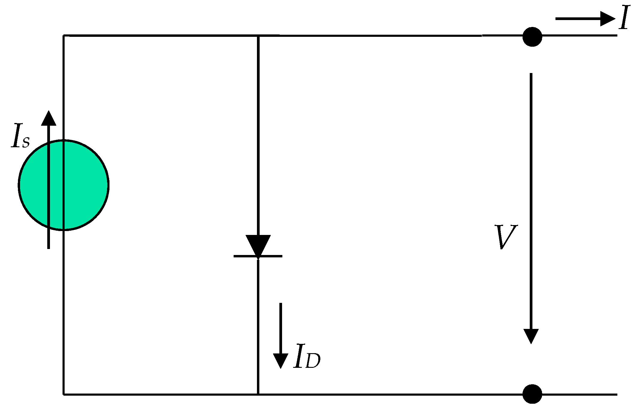
It is assumed that the electrical behavior of a PV module can be described by the equivalent circuit shown in
Figure 2.
The p–n junction performs as a large diode. The fundamental property of a diode is that it conducts electric current in only one direction. When the applied voltage is positive and greater than a certain minimum, then the current flows through the diode. If the voltage is negative, then the diode does not conduct current, at least until a certain voltage is reached.
Current
is the current across a diode, whose equation is as follows:
where
is the diode’s inverse saturation current,
is the terminal voltage, and
is the diode’s ideality factor (ideal diode:
; real diode:
).
Still regarding Equation (1),
is the thermal voltage in
V, given by the following:
where
is the Boltzmann constant (
),
is the absolute temperature in
K, and
is the electron’s electrical charge (
). For the STC temperature, it is
.
Current is modeled by a current source and is the current generated by the photovoltaic effect; this current flows always in the same direction and is constant as long as the irradiance is also constant. As mentioned, the p–n junction operates as a diode crossed by a unidirectional internal current , which depends on the terminal voltage .
Referring to
Figure 2, current
is as follows:
It is noted that the source current, , is equal to the short-circuit current, , as can be seen from Equation (3), by setting .
For a given irradiance and module temperature, the electrical
DC output power,
, is as follows:
The maximum power is obtained when
, which leads to the following:
It is known that PV modules operate always at the maximum possible power for the given irradiance and temperature, this optimal operation being achieved due to the Maximum Power Point Tracker (MPPT). Therefore, the computation of the PV module maximum power is very important.
The solution to Equation (5) is
, the maximum power voltage, and the corresponding current is
, the maximum power current, respectively given by the following:
The maximum power is . stresses that the output power is DC.
As Equation (6) is a non-linear equation, its solution requires iterative methods. If Gauss–Seidel is used, the required iterative equation to be solved is (
is the iteration number):
To solve Equation (8), the knowledge of an initial guess, , and of the three parameters , , and is required. It is recalled that the thermal voltage is known because it depends solely on the module temperature, which is assumed to be known.
A proper starting guess is
. To determine the three parameters of the 1D + 3P model, let us write the fundamental Equation (3) at the short-circuit (
), open-circuit (
), and maximum power (
) points, respectively, and at STCs. The following three equations are obtained:
It is important to highlight that the 3 parameters of the model can be computed solely based on datasheet open information, as can be verified in
Table 1. The short-circuit parameter is directly obtained from the datasheet.
The influence of the irradiance and module temperature in the 1 diode and 3 parameters model is accounted for by considering the following:
The ideality factor is constant ;
The short-circuit current, , holds the variation of the irradiance;
The module temperature influence is incorporated in the inverse saturation current, .
Experimental results show the validity of these approximations.
Therefore, for any temperature and irradiance given conditions, Equation (8) can be written as follows:
It is possible to demonstrate that the simplest model accounts for the inverse saturation current dependence on the temperature by using the following equation:
where
is a constant,
is the silicon bandgap and
is the number of series-connected cells in a PV module. The value of
is not relevant, because one can write Equation (13) at STCs and obtain the following:
As for the influence of the irradiance on the short-circuit current, the simplest model is going to be used, which states that the short-circuit current is linearly dependent on the irradiance:
It is noted that the dependence of the short-circuit current on the temperature has been disregarded. This dependence is reflected on the short-circuit temperature coefficient that most of the time is provided in the manufacturer’s datasheet. However, temperature coefficients are not always displayed in the datasheets, some manufacturers opting not to provide them. As the main feature of the developed model is to be based solely on readily available manufacturer’s data, it was decided not to include the temperature coefficients as input data for the model. Nevertheless, the dependence of the short circuit current on the temperature is weak, in the magnitude order of about 0.05%/°C.
It is now possible to compute the maximum power voltage for any irradiance and temperature conditions, iteratively solving Equation (12), taking into account Equation (2), Equation (10), Equation (11), Equation (14) and Equation (15). After
is obtained, the maximum power current is computed through the following (see Equation (7)):
The
DC power output is as follows:
2.2. The Proposed Model: Simplified 1 Diode and 3 Parameters Model
In this paper, a simplified version of the classical 1 diode and 3 parameters model is proposed. The main feature of the proposed simplification is to avoid the need for solving a non-linear equation. This is an important feature that speeds up the process of computing the PV module power output for any given irradiance and module temperature.
Let us look again at Equation (16). We notice that it can be written as follows:
The issue in this equation is that
depends on
. If the aim is to simplify the computation process, a simplification can be introduced to overcome this problem. As so, let us assume the maximum power current changes linearly with the irradiance, as we have assumed for the short-circuit current:
This considerably simplifies the computation process, as now
can be easily calculated, without the need for iterations.
The DC power output is obtained from the multiplication of algebraic Equations (19) and (20).
3. Results
In this section, the validation of the above introduced two models is performed. This validation takes place by comparing the results provided by both models with experimental data available in a comprehensive PV modules database and the theoretical results obtained by using a widely known PV modules simulation software that uses the 1D + 5P model.
3.1. Validation against the CEC Database
The California Energy Commission (CEC) owns a comprehensive PV modules database with more than 20,000 entries. The database is openly available from Reference [
22]. Each entry includes the following main information:
Technology of the module (monocrystalline, polycrystalline, and thin film).
Dimensions of the module (short-side length and long-side length).
PV module datasheet, i.e., the information displayed in
Table 1.
Temperature coefficients of the maximum power voltage and maximum power current.
Experimental maximum power current and maximum power voltage for Low-Irradiance Conditions.
Experimental maximum power current and maximum power voltage for NOCs.
Computed output power for PVUSA test conditions, using a detailed one diode and five parameters model.
The database contains experimental data and computed results at different operating conditions. These are as follows:
A first filtering was performed to the database to purge wrong data. For instance, the following errors were identified in the database:
Maximum power current (voltage) at STCs greater than the short-circuit current (open circuit voltage) at STCs.
Power output at NOCs greater than the peak power.
Power output at PVUSA test conditions greater than peak power.
The database was then divided according to the technology of the PV modules. A grand total of 17,300 PV modules was selected, composed of 8700 monocrystalline modules, 8300 polycrystalline modules, and 330 thin-film modules.
Figure 3 displays the peak power histograms of the three considered technologies.
The main idea behind the building of the database used in this work was to consider only standard modules that are commonly sold worldwide. Experimental modules, with several branches in parallel to increase the output power, were disregarded as they do not represent readily available technology. Only two modules with a nameplate power higher than 500 Wp were considered because they use only one branch in parallel. These two modules use thin-film technology.
The difference in the number of modules in
Figure 3 with respect to the number of modules in
Figure 4,
Figure 5,
Figure 6,
Figure 7,
Figure 8,
Figure 9,
Figure 10,
Figure 11 and
Figure 12 is due to invalid results obtained for several modules stemming from the reasons presented above, which showed incongruencies in the input data values. Therefore, the modules showing wrong data in the initial sample (
Figure 3) were removed from the set of results obtained (
Figure 4,
Figure 5,
Figure 6,
Figure 7,
Figure 8,
Figure 9,
Figure 10,
Figure 11 and
Figure 12).
No information concerning the tolerance of the manufacturer datasheet was given in the California Energy Commission (CEC) database. Therefore, the data tolerance was not taken into consideration.
The modules’ power output provided by the one diode and three parameters (PDC1) model and by the simplified one diode and three parameters (PDC2) were compared against the corresponding data contained in the CEC database. The comparisons were performed for the three following operating conditions regarding irradiance and temperature:
NOC: and .
PVUSA: and .
Low: and .
The objective of the tests performed is twofold. On one hand, it is desired to assess the performance of the 1D + 3P against the data provided in the database for the three abovementioned operating conditions. On the other hand, a comparison of the performance of the simplified 1D + 3P model against the 1D + 3P model is intended.
3.1.1. Results of the Tests at Normal Operating Conditions
The Percentage Error
, for each module, and the Mean Absolute Percentage Error
, for the entire sample, metrics were used to assess the performed tests.
where
is the
DC output power computed by the 1D + 3P model at NOCs,
is the output
DC power computed by the simplified 1D + 3P model at NOCs and
is the experimental
DC output power at NOCs, as given in the CEC database.
Figure 4 displays the histograms of the Percentage Error
concerning
and
and the Percentage Error
concerning
and
(see Equations (22) and (23)) both for the monocrystalline modules sample. The
y-axis shows the number of times each Percentage Error interval represented on the
x-axis occurs in the considered sample.
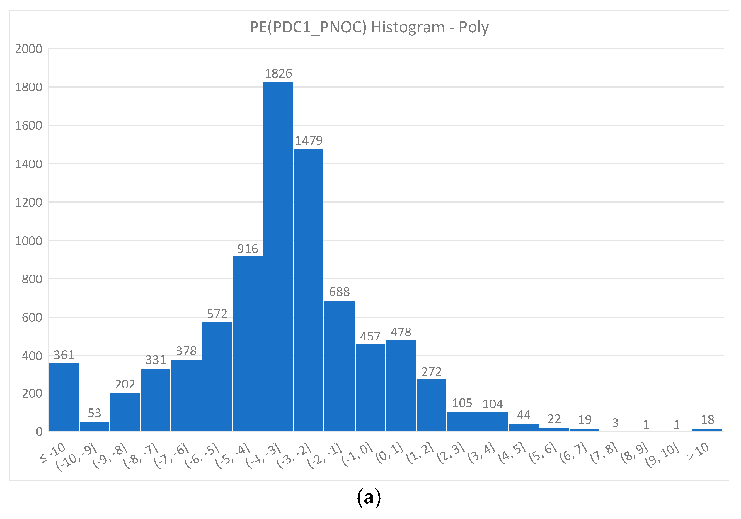
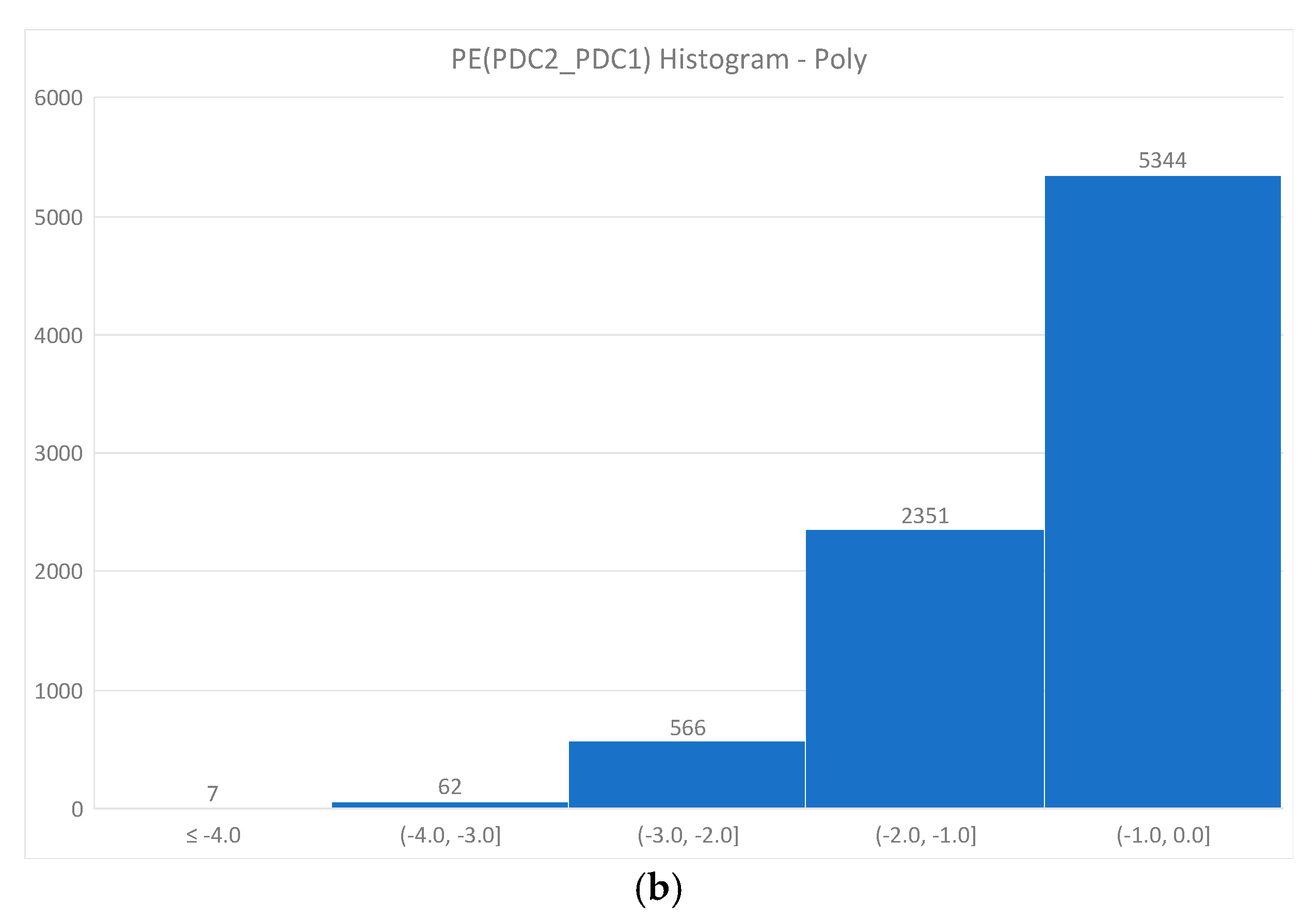
Figure 5 displays the same metrics for the polycrystalline (Poly) modules, whereas
Figure 6 is concerned with thin films (TFs).
The Mean Absolute Percentage Error (
MAPE) (see Equations (24)–(26)) concerning monocrystalline, polycrystalline, and thins films under NOCs are shown in
Table 2.
From the set of results presented above, it is possible to conclude that the 1D + 3P model can estimate the output power of the PV modules with a reasonable degree of accuracy, at Normal Operating Conditions. For the monocrystalline and polycrystalline modules, a MAPE of less than 4% is obtained; for the thin films’ modules, the MAPE increases to values of about 7%. In what concerns the ability of the simplified 1D + 3P model following the 1D + 3P model in Normal Operating Conditions, the results are encouraging. The MAPE is less than 1% for both monocrystalline and polycrystalline modules and slightly increases to 1.4% when thin films are considered.
The analysis of the histograms reveals that several outliers are still present in the samples. Many of these outliers result from wrong data in the samples that were not removed in the purging performed in the original database. Other outliers, however, result from the individual parameters at STCs, used to build the models, that lead to poor estimates.
Another observation is that the 1D + 3P model predicts, in general, a lower output power than the experimental results, at Normal Operating Conditions. On the other hand, the 1D + 3P simplified model always predicts lower values of the output power than the original 1D + 3P model, therefore making the Percentage Error negative.
3.1.2. Results of the Tests at Low Irradiance
As in the assessment of the NOCs case, the Percentage Error
, for each module, and the Mean Absolute Percentage Error
, for the entire sample, metrics were used in the experiments conducted at Low-Irradiance Conditions. These indexes are defined for this case as follows:
where
is the output DC power computed by the 1D + 3P model at Low-Irradiance Conditions (
Low),
is the output DC power computed by the simplified 1D + 3P model at
Low and
is the experimental DC output power at Low as given in the CEC database.
Figure 7 displays the histograms of the Percentage Error
concerning
and
and the Percentage Error
concerning
and
both for the monocrystalline modules sample.
Identical information is displayed in
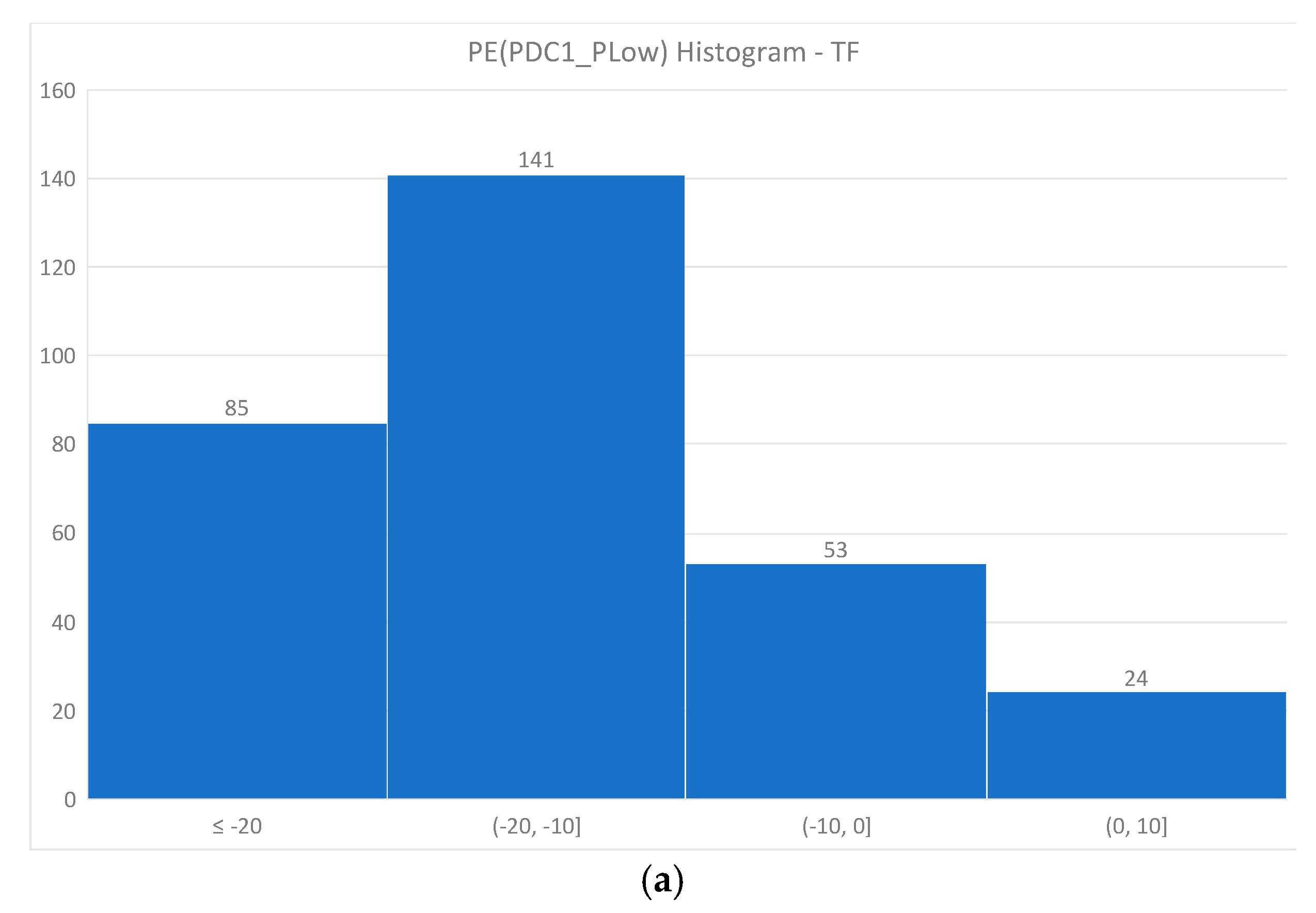
Figure 8 for the polycrystalline (Poly) modules, whereas
Figure 9 is concerned with thin films (TFs).
The Mean Absolute Percentage Error (
results concerning monocrystalline, polycrystalline, and thin films under Low-Irradiance Conditions are shown in
Table 3.
Regarding the ability of the 1D + 3P model to follow the experimental results at Low-Irradiance Conditions, the conclusions are a bit different from the ones at Normal Operation Conditions. The MAPE has increased significantly from around 4% to around 10%, for crystalline silicon modules and from 7% to 16% for thin films. This means that the 1D + 3P model shows some difficulties in forecasting the output power at these conditions. However, the approximation provided by the simplified 1D + 3P remains very good, in the same order of magnitude, i.e., around 1%. This allows the conclusion that the simplified 1D + 3P model offers a good approximation, yet much simpler, of the original 1D + 3P model.
Once again, it is verified the presence of several outliers in the samples, the reasons being the same as previously explained.
At Low-Irradiance Conditions, the 1D + 3P model estimates the real output power by default. The same behavior is observed as far as the simplified 1D + 3P model in relation to the 1D + 3P model is concerned.
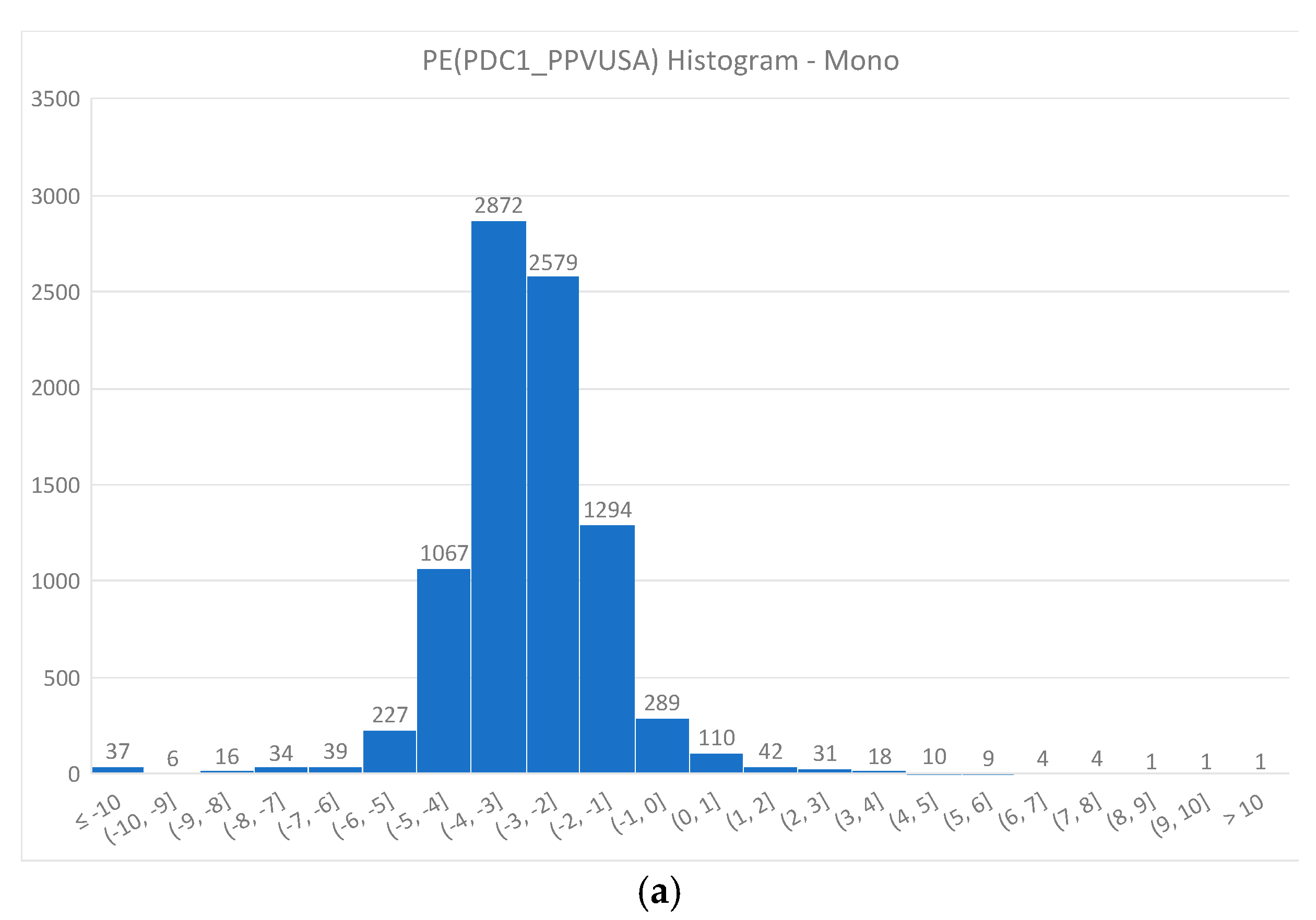
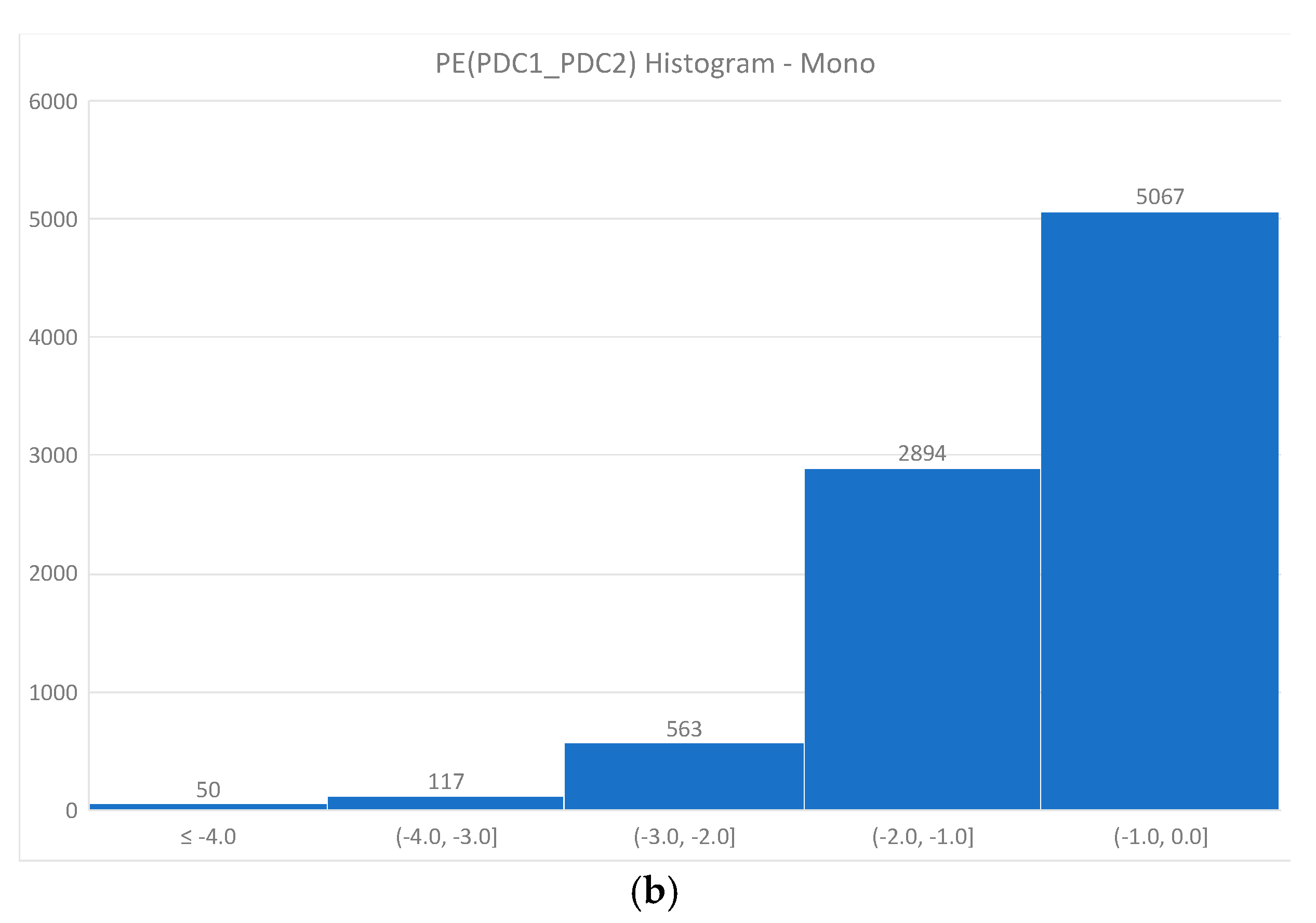
3.1.3. Results of the Tests at PVUSA Conditions
The results obtained at PVUSA conditions were very similar to the ones obtained at Normal Operating Conditions. In fact, the irradiance and module temperature are similar, this explaining the similitude of results.
The definition of the assessment indexes is as follows:
where
is the output DC power computed by the 1D + 3P model at
PVUSA conditions (
PVUSA),
is the output DC power computed by the simplified 1D + 3P model at
PVUSA and
is the computed DC output power using a detailed model, as given in the CEC database. It is stressed that the power
provided at CEC database is not an experimental value, but instead, a computed value using the detailed 1D + 5P model.
Figure 10 displays the histograms of the Percentage Error
concerning
and
and the Percentage Error
concerning
and
both for the monocrystalline modules sample. The same information is shown in
Figure 11 for the polycrystalline (Poly) modules, and in
Figure 12 for the thin films (TFs).
The Mean Absolute Percentage Error (
results concerning monocrystalline, polycrystalline, and thin films under
PVUSA conditions are shown in
Table 4.
It should be noted that, for the PVUSA conditions, the 1D + 5P is being used for comparison purposes and not experimental results like in NOCs and Low. The accuracy of the 1D + 5P should be taken into consideration to assess the deviations to experimental results. However, it is not possible to assess the said accuracy because no experimental results are available for PVUSA conditions.
3.1.4. Note on Bifacial PV Modules
A final note on bifacial PV modules. The database contained three thin-film bifacial PV modules with peak power equal to 490, 500, and 510 Wp. The developed models were applied to the PV modules with this technology, with the purpose of assessing the accuracy of the models to describe the modules’ behavior in
NOC,
PVUSA and Low conditions.
Table 5 shows the Percentage Errors (of
in relation to
and of
in relation to
) achieved for the three modules under the said conditions.
As far as NOC and PVUSA conditions are concerned, the bifacial PV modules Percentage Errors are consistent with the obtained for thin-film modules. However, in what concerns Low-Irradiance Conditions the percentage error is much higher than the corresponding for thin films. This is an indication of the difficulties of both the 1D + 3P and its simplified version in reproducing the behavior of the bifacial PV modules under Low-Irradiance Conditions.
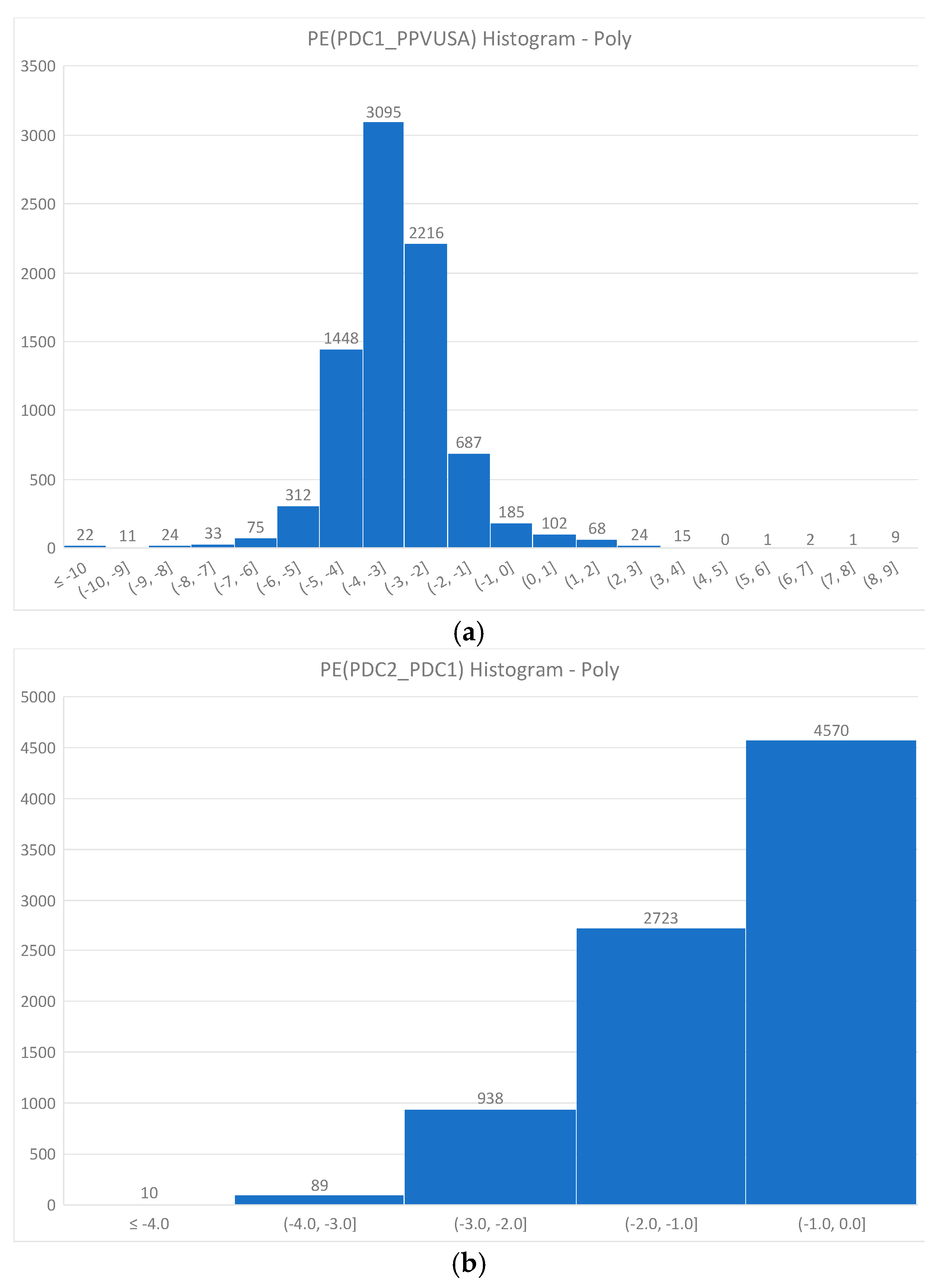
3.2. Validation against PVsyst
Another set of the 1D + 3P and simplified 1D + 3P models was performed using PVsyst software [
23] as the benchmark. PVsyst is a powerful tool to design PV systems. To describe the behavior of the PV modules, it uses the one diode and five parameters model, which is well adapted for crystalline silicon technologies, but needs some adaptations when addressing thin-film technologies. This characteristic of PVsyst models will be important later.
A sample with 82 PV modules (31 monocrystalline, 31 polycrystalline, and 20 thin films) was considered. The variation of the modules peak power is shown in
Table 6.
The same set of tests as performed for the CEC database was also performed with the said sample using PVsyst software. Tests were conducted for
NOC,
Low, and
PVUSA conditions. The performance of the 1D + 3P model was compared to PVsyst’s one by computing the PV module output power at the considered conditions. Moreover, the ability of the simplified 1D + 3P model to follow the 1D + 3P model was assessed. The
MAPE metric was again used to evaluate the accuracy of both estimations. It is stressed that PVsyst uses a detailed 1D + 5P model to compute the DC output power.
Table 7,
Table 8, and
Table 9 display the obtained results.
In general, the results obtained with PVsyst are in line with the ones obtained with the CEC database. The errors are of the same order of magnitude, namely for crystalline silicon modules. However, it is observed that, for the thin-film modules, the MAPE obtained with the PVSyst validation is lower than the one obtained with the CEC database validation. This can be explained by the abovementioned difficulties of the PVsyst model to accurately represent thin-film modules. The 1D + 5P model used by PVsyst estimates a lower DC output power than the real one. The 1D + 3P model does the same, but worse. Therefore, the MAPE concerning the performance of both models is reduced. A common feature between the PVsyst and CEC database validations is the small MAPE (around 1%) obtained for the comparison between the estimates of the 1D + 3P model and the simplified 1D + 3P model.
4. Discussion
One of the objectives of this paper was to assess the validity limits of the one diode and three parameters model. The validation against experimental data was carried out by using the CEC database, for two operating points: Normal Operating Conditions and Low-Irradiance Conditions. For the former conditions, it was found a satisfactory agreement between theoretical predictions and experimental results. A MAPE of less than 4% was found for both monocrystalline and polycrystalline modules, the MAPE for thin films being a little bit higher (about 7%). For the latter conditions, the MAPE increased, exposing the difficulties of the 1D + 3P model to reproduce the experimental results for these operating conditions. MAPE values of around 10% were found for the monocrystalline and polycrystalline technologies, the MAPE for thin films being even higher (about 15%).
Moreover, the 1D + 3P was tested against a more detailed model (1D + 5P) implemented in the well-known software PVsyst. The same pattern was found in this test. For the NOCs, the MAPE was about 3% for both monocrystalline and polycrystalline cells and about 4% for thin films. For the Low-Irradiance Conditions, the MAPE increased, as it was observed in the CEC database validation, to around 10%, for mono and poly cells, and to 13% for thin films.
For the PVUSA conditions, only theoretical results were available both in the CEC database and in PVsyst. The obtained results show some discrepancy which may result from different detailed models being used. When comparing to the model implemented in the CEC database, the MAPE is around 3% for both silicon technologies and increases to 10% when the thin films are concerned. Much smaller errors are obtained when comparing with PVsyst: 1% for silicon and 3% for thin films.
All in all, the conclusion is that the 1D + 3P model is a valid representation of the behavior of a PV module in normal operating conditions (MAPE around 3%). For Low Irradiance, the performance of the 1D + 3P model decreases, a MAPE of about 10% being expected. It is worth mentioning that most of the time, the approximations of the 1D + 3P model are made by default.
Another aim of the paper was to assess if a simplification made in the 1D + 3P model, that greatly simplifies the involved mathematics, is a good representation of the full 1D + 3P model that requires the solution of a non-linear equation. The conclusion is a clear yes. Considering all the simulations performed, the MAPE was always around 1%, regardless of the considered technology. No significant changes in the performance of the simplified 1D + 3P model were found considering the validation against experimental or theoretical results. Therefore, it is possible to use the simplified 1D + 3P model as an inexpensive tool to predict the electrical behavior of PV modules, because it provides a very similar output to the one supplied by the original 1D + 3P model.
To allow the reproducibility of the tests performed in this paper,
Table 10 is offered. In this Table, the characteristics of three PV modules, one for each technology, are presented, together with the respective relevant data retrieved from the manufacturer’s datasheet at STCs. These data are necessary to compute the 1D + 3P model parameters. These parameters and the electrical quantities (voltage, current and power) obtained with the simplified 1D + 3P model are displayed, as well as the corresponding PVsyst outputs, found in the same simulation conditions. Finally, the Percentage Error of the maximum power voltage, maximum power current and output power is also shown. The comparison is performed for the Normal Operating Conditions and for the Low-Irradiance Conditions.
Analyzing the Percentage Error displayed in
Table 10, it is possible to conclude that the output power estimations by the simplified 1D + 3P model are achieved by default, which was already concluded before. However, it is interesting to note that, in general, the voltage predictions are made by default, whereas the current estimations are made by excess.


