
A Step-by-Step Design for Low-Pass Input Filter of the Single-Stage Converter


Abstract
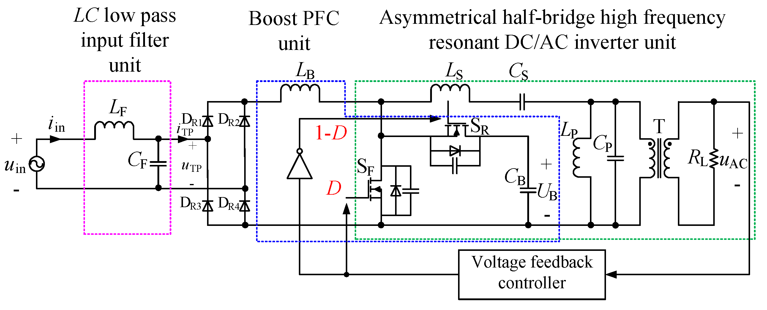
:1. Introduction
2. Circuit Analysis
2.1. Known and Preset Parameters of the Input Filter
- (1)
- No harmonics are contained in the input voltage.
- (2)
- The energy-stored capacitor CB is large enough so that its voltage ripple can be ignored and hence the duty cycle D of the switch SF is assumed to remain constant during half line cycle.
- (3)
- The input power of the converter Pin is equal to the output power P, which means the efficiency of the converter is supposed to be 100%, that is, η = 100%. In practical applications, the efficiency is less than 100%. Then it only needs to add corresponding coefficients between input and output for analysis, that is, Pin = P/η.
- (4)
- Because of the pulse-width modulation, the dominant harmonic components of the input current occur at or around the switching frequency and its multiples. The former is the main component. Hence, assume that all the energy in the input current spectrum is concentrated on the switching frequency.
- (1)
- m is the ratio of the fundamental component amplitude UTPFm of the voltage across the AC side of the rectifier bridge to the voltage UB across the stored-energy capacitor CB. In addition, m must be slightly smaller than 0.9. One reason is that, considering the Boost-type PFC operating in DCM, the input power factor of the rectifier bridge can be ensured larger than 0.9 on condition that m is smaller than 0.9 [38]. Another reason is that a smaller m means a larger UB; m = 0.8 is chosen for comprehensive consideration.
- (2)
- The input fundamental power factor λF: to minimize the influence on the input power factor of the input filter, the phase angle must be small at fundamental frequency, so λF should be close to 1. Here, λF can be taken as 0.99 ≤ λF ≤ 1.
- (3)
- α is the ratio of the RMS value UTPF of the voltage drop uTP in fundamental component to the RMS value Uin of the input voltage uin. Additionally, α must be close to unity so that the voltage drop in the fundamental component across the filter is small, and an enhanced efficiency can be obtained as well as power density. Therefore, α can be taken as 0.98 ≤ α ≤ 1.02.
- (4)
- For the voltage drop uTP across the AC side of the rectifier bridge, β is the ratio of the RMS value UTPSW of the harmonic component at the switching frequency to the RMS value UTPF of the component at the grid frequency. In addition, β should be set within a small limit so that the input voltage of SSC has a limited amount of high harmonic ripple UTPSW to ensure the proper operation of the SSC. Therefore, β can be taken as 0.0005 ≤ β ≤ 0.005.
- (5)
- For the input current, γ is the ratio of the RMS value ITPSW of the harmonic component at the switching frequency to the RMS value ITPF of the fundamental component at grid frequency. It should be set within a small limit to reduce the harmonic current at the switching frequency. Therefore, γ can be taken as 0.0001 ≤ γ ≤ 0.001.
2.2. Equivalent Circuit of SSC
2.3. The RMS Value of the Current at Switching Frequency on the AC Side of the Rectifier—ITPSW
3. Parameter Design
3.1. Step-by-Step Design Analysis
- (a)
- the input line frequency current is in phase with the input voltage (resistive input current).
- (b)
- the input line frequency current leads the input voltage (capacitive input current).
- (c)
- the input line frequency current lags the input voltage (inductive input current).
- (a)
- Resistive input current
- (b)
- Capacitive input current
- (c)
- Inductive input current
3.2. A Design Example
4. Sensitivity Analysis of LC Filter
- ①
- As shown in (41), > 0, > 0, < 0. It can be seen that LF increases with increasing α and β. In addition, LF decreases with increasing γ.
- ②
- Similarly, < 0, < 0, > 0. It can be seen that CF decreases with the increase of α and β. In addition, CF increases with the increase of γ.
- ③
- It can also be seen that α has the greatest impact on LF, and the normalized sensitivity of β and γ to LF are similarly small. In addition, α and β have similar influences on CF, and γ has the smallest effect on CF. As α has such a big influence on LF, Figure 13 shows the relationship between and α.
5. Simulation Results
6. Experimental Results
7. Conclusions
- (1)
- The paper offers a quantitative parameter design method with several references. Therefore, me references just give the direction on how to design and adjust or design procedure with try and error method, which is complicated and time-consuming. The proposed method is a programmatic step-by-step design method, which is an easy-to-use tool for designing an LC input filter. Meanwhile, the precise design method is based on the restrictions of the input harmonic currents, so an accurate analytical design procedure is presented.
- (2)
- The sensitivity analysis provides a method that can accurately adjust input filter parameters to the expected value, and the performance can be satisfied at the same time.
Author Contributions
Funding
Institutional Review Board Statement
Informed Consent Statement
Data Availability Statement
Conflicts of Interest
Appendix A
| Symbol | Explanation |
| uin | input voltage |
| Uin | the RMS value of uin |
| uTP | the voltage drop across the AC side of the diode rectifier bridge |
| uTPF | the component of uTP at the grid frequency |
| UTPF | the RMS value of uTPF |
| UTPFm | the amplitude value of UTPF |
| uTPSW | the harmonic component of uTP at the switching frequency |
| UTPSW | the RMS value of uTPSW |
| iin | input current |
| iinF | the component of iin at the grid frequency |
| IinF | the RMS value of iinF |
| iinSW | the component of iin at the switching frequency |
| IinSW | the RMS value of iinSW |
| iTP | the input current of the AC side of the diode rectifier bridge |
| iTPF | the component of iTP at the grid frequency |
| ITPF | the RMS value of iTPF |
| iTPSW | the component of iTP at the switching frequency |
| ITPSW | the RMS value of iTPSW |
| RTPF | an equivalent resistor of the output of the LC filter at the grid frequency |
| UB | the voltage across the stored-energy capacitor |
| m | m =UTPFm/UB |
| φ | the input grid frequency current iinF lags the input voltage with angle φ |
| λF | the fundamental power factor λF = cosφ |
| α | α = UTPF/Uin |
| β | β = UTPSW/UTPF |
| γ | γ = IinSW/ITPF |
Appendix B
Appendix C
References
- Mayordomo, J.G.; Beites, L.F.; Yang, X.; Xu, W. A Detailed Procedure for Harmonic Analysis of Three-Phase Diode Rectifiers Under Discontinuous Conduction Mode and Nonideal Conditions. IEEE Trans. Power Deliv. 2018, 33, 741–751. [Google Scholar] [CrossRef]
- Du, Y.; Wang, J.; Wang, G.; Huang, A.Q. Modeling of the High-Frequency Rectifier With 10-kV SiC JBS Diodes in High-Voltage Series Resonant Type DC–DC Converters. IEEE Trans. Power Electron. 2014, 29, 4288–4300. [Google Scholar] [CrossRef]
- Liu, J.; Liu, Z. Harmonic Analyzing of the Double PWM Converter in DFIG Based on Mathematical Model. Energies 2017, 10, 2087. [Google Scholar] [CrossRef] [Green Version]
- Liu, Y.; Xu, J.; Shuai, Z.; Li, Y.; Peng, Y.; Liang, C.; Cui, G.; Hu, S.; Zhang, M.; Xie, B. A Novel Harmonic Suppression Traction Transformer with Integrated Filtering Inductors for Railway Systems. Energies 2020, 13, 473. [Google Scholar] [CrossRef] [Green Version]
- Raizer, A.; Silva, J.V.D.; Fonseca, M.P. Analysis of harmonic current emissions in voltages below the presented by the Standard IEC 61000-3-2. In Proceedings of the 2017 IEEE 3rd Global Electromagnetic Compatibility Conference (GEMCCON), Sao Paulo, Brazil, 8–10 November 2017; pp. 1–4. [Google Scholar]
- Cao, K.; Liu, X.; He, M.; Meng, X.; Zhou, Q. Active-Clamp Resonant Power Factor Correction Converter With Output Ripple Suppression. IEEE Access 2021, 9, 5260–5272. [Google Scholar] [CrossRef]
- Li, H.; Li, S.; Xiao, W. Single-Phase LED Driver With Reduced Power Processing and Power Decoupling. IEEE Trans. Power Electron. 2021, 36, 4540–4548. [Google Scholar] [CrossRef]
- Huynh, P.S.; Ronanki, D.; Vincent, D.; Williamson, S.S. Direct AC–AC Active-Clamped Half-Bridge Converter for Inductive Charging Applications. IEEE Trans. Power Electron. 2021, 36, 1356–1365. [Google Scholar] [CrossRef]
- Wang, Y.; Deng, X.; Wang, Y.; Xu, D. Single-Stage Bridgeless LED Driver Based on a CLCL Resonant Converter. IEEE Trans. Ind. Appl. 2018, 54, 1832–1841. [Google Scholar] [CrossRef]
- Ali, K.; Dube, S.K.; Das, P.; Peng, J.C.; Rogers, D.J. Improvement of ZVS Range and Current Quality of the Nine-Switch Single-Stage AC–DC Converter. IEEE Trans. Power Electron. 2020, 35, 4658–4668. [Google Scholar] [CrossRef]
- Alayi, R.; Zishan, F.; Mohkam, M.; Hoseinzadeh, S. A Sustainable Energy Distribution Configuration for Microgrids Integrated to the National Grid Using Back-to-Back Converters in a Renewable Power System. Electronics 2021, 10, 1826. [Google Scholar] [CrossRef]
- Hoseinzadeh, S.; Ghasemi, M.H.; Heyns, S. Application of hybrid systems in solution of low power generation at hot seasons for micro hydro systems. Renew. Energy 2020, 160, 323–332. [Google Scholar] [CrossRef]
- Narimani, M.; Moschopoulos, G. A New Interleaved Three-Phase Single-Stage PFC AC–DC Converter. IEEE Trans. Ind. Electron. 2014, 61, 648–654. [Google Scholar] [CrossRef]
- Alonso, J.M.; Dalla Costa, M.A.; Ordiz, C. Integrated Buck-Flyback Converter as a High-Power-Factor Off-Line Power Supply. IEEE Trans. Ind. Electron. 2008, 55, 1090–1100. [Google Scholar] [CrossRef]
- Mishima, T.; Sakamoto, S.; Ide, C. ZVS Phase-Shift PWM-Controlled Single-Stage Boost Full-Bridge AC–AC Converter for High-Frequency Induction Heating Applications. IEEE Trans. Ind. Electron. 2017, 64, 2054–2061. [Google Scholar] [CrossRef] [Green Version]
- Kim, J.; Choi, H.; Won, C. New Modulated Carrier Controlled PFC Boost Converter. IEEE Trans. Power Electron. 2018, 33, 4772–4782. [Google Scholar] [CrossRef]
- Xu, H.; Chen, D.; Xue, F.; Li, X. Optimal Design Method of Interleaved Boost PFC for Improving Efficiency from Switching Frequency, Boost Inductor, and Output Voltage. IEEE Trans. Power Electron. 2019, 34, 6088–6107. [Google Scholar] [CrossRef]
- Narimani, M.; Moschopoulos, G. Analysis and design of a new three-level PFC AC-DC converter. In Proceedings of the 2013 IEEE Energy Conversion Congress and Exposition, Denver, CO, USA, 15–19 September 2013; pp. 4808–4813. [Google Scholar]
- Lee, S.; Do, H. Soft-Switching Two-Switch Resonant AC–DC Converter With High Power Factor. IEEE Trans. Ind. Electron. 2016, 63, 2083–2091. [Google Scholar] [CrossRef]
- Golbon, N.; Moschopoulos, G. A Low-Power AC–DC Single-Stage Converter With Reduced DC Bus Voltage Variation. IEEE Trans. Power Electron. 2012, 27, 3714–3724. [Google Scholar] [CrossRef]
- Luo, Q.; Ma, K.; He, Q.; Zou, C.; Zhou, L. A Single-Stage High-Frequency Resonant AC/AC Converter. IEEE Trans. Power Electron. 2017, 32, 2155–2166. [Google Scholar] [CrossRef]
- Luo, Q.; Zhi, S.; Zou, C.; Lu, W.; Zhou, L. An LED Driver With Dynamic High-Frequency Sinusoidal Bus Voltage Regulation for Multistring Applications. IEEE Trans. Power Electron. 2014, 29, 491–500. [Google Scholar] [CrossRef]
- Lee, M.; Lai, J.-S. Spread-Spectrum Frequency Modulation With Adaptive Three-Level Current Scheme to Improve EMI and Efficiency of Three-Level Boost DCM PFC. IEEE Trans. Power Electron. 2021, 36, 2476–2480. [Google Scholar] [CrossRef]
- Lee, M.; Lai, J.-S. Unified Voltage Balancing Feedforward for Three-Level Boost PFC Converter in Discontinuous and Critical Conduction Modes. IEEE Trans. Circuits Syst. II Exp. Briefs 2021, 68, 441–445. [Google Scholar] [CrossRef]
- Yao, K.; Hu, W.; Li, Q.; Lyu, J. A Novel Control Scheme of DCM Boost PFC Converter. IEEE Trans. Power Electron. 2015, 30, 5605–5615. [Google Scholar] [CrossRef]
- Xiang, Z.; Pang, Y.; Wang, L.; Wong, C.; Lam, C.; Wong, M. Design, control and comparative analysis of an LCLC coupling hybrid active power filter. IET Power Electron. 2020, 13, 1207–1217. [Google Scholar] [CrossRef]
- Shafiei, N.; Pahlevaninezhad, M.; Farzanehfard, H.; Motahari, S.R. Analysis and Implementation of a Fixed-Frequency LCLC Resonant Converter With Capacitive Output Filter. IEEE Trans. Ind. Electron. 2011, 58, 4773–4782. [Google Scholar] [CrossRef]
- Lin, R.; Huang, L. Efficiency Improvement on LLC Resonant Converter Using Integrated LCLC Resonant Transformer. IEEE Trans. Ind. Appl. 2018, 54, 1756–1764. [Google Scholar] [CrossRef]
- Pini, S.; Barbi, I. A single-phase high-power-factor rectifier, based on a two-quadrant shunt active filter. IEEE Trans. Power Electron. 2011, 26, 3131–3143. [Google Scholar] [CrossRef]
- Senturk, O.S.; Hava, A.M. Performance enhancement of the single-phase series active filter by employing the load voltage waveform reconstruction and line current sampling delay reduction methods. IEEE Trans. Power Electron. 2011, 26, 2210–2220. [Google Scholar] [CrossRef]
- Tang, Y.; Loh, P.; Wang, P.; Choo, F.; Gao, F. Exploring inherent damping characteristic of LCL-filters for three-phase grid-connected voltage source inverters. IEEE Trans. Power Electron. 2012, 27, 1433–1443. [Google Scholar] [CrossRef]
- Iftikhar, M.U.; Sadarnac, D.; Karimi, C. Input filter damping design for control loop stability of DC–DC converters. In Proceedings of the 2007 IEEE International Symposium on Industrial Electronics, Vigo, Spain, 4–7 June 2007; pp. 353–358. [Google Scholar]
- Yu, X.; Salato, M. An Optimal Minimum-Component DC–DC Converter Input Filter Design and Its Stability Analysis. IEEE Trans. Power Electron. 2014, 29, 829–840. [Google Scholar]
- Guo, W.; Jain, P.K. A low frequency AC to high frequency AC inverter with build-in power factor correction and soft-switching. IEEE Trans. Power Electron. 2004, 19, 430–442. [Google Scholar] [CrossRef]
- Liserre, M.; Blaabjerg, F.; Hansen, S. Design and control of an LCL-filter-based three-phase active rectifier. IEEE Trans. Ind. Appl. 2005, 41, 1281–1291. [Google Scholar] [CrossRef]
- Jalili, K.; Bernet, S. Design of LCL Filters of Active-Front-End Two-Level Voltage-Source Converters. IEEE Trans. Ind. Electron. 2009, 56, 1674–1689. [Google Scholar] [CrossRef]
- Basu, K.; Sahoo, A.K.; Chandrasekaran, V.; Mohan, N. Grid-Side AC Line Filter Design of a Current Source Rectifier With Analytical Estimation of Input Current Ripple. IEEE Trans. Power Electron. 2014, 29, 6394–6405. [Google Scholar] [CrossRef]
- Athab, H.S.; Lu, D.D. A High-Efficiency AC/DC Converter With Quasi-Active Power Factor Correction. IEEE Trans. Power Electron. 2010, 25, 1103–1109. [Google Scholar] [CrossRef]
- Sahoo, A.K.; Basu, K.; Mohan, N. Systematic Input Filter Design of Matrix Converter by Analytical Estimation of RMS Current Ripple. IEEE Trans. Ind. Electron. 2015, 62, 132–143. [Google Scholar] [CrossRef]
- ENERGY STAR: Program Requirements for Solid State Lighting Luminaires; Environmental Protection Agency and U.S. Department of Energy: Washington, DC, USA, 2008. Available online: https://www.osti.gov/biblio/1218258-energy-star-program-requirements-solid-state-lighting-luminaires (accessed on 1 November 2021).
- Lloyd, H. Dixon, Unitrode Magnetics Design Handbook; Texas Instruments: Dallas, TX, USA, 2001. [Google Scholar]


| Ref. | Filter Type | Application | Quantitative Design | |
|---|---|---|---|---|
| [33] | DC Input filter | LC | DC/DC converter | No |
| [34] | DC Bus filter | C + LC | DC/AC stage of the AC/AC converter | No |
| [35] | AC Input filter | LCL | Three-phase active rectifier | No |
| [36] | AC Input filter | L/LCL | Three-phase active rectifier | Yes |
| [37] | AC Input filter | LC | Three-phase current source rectifier | Yes |
| Proposed | AC Input filter | LC | Single-phase single-stage converter | Yes |
| Specifications | Value |
|---|---|
| Input voltage uin | 220 VAC/50 Hz |
| Output Power P = Pin | 130 W |
| Switching frequency fSW | 100 kHz |
| m = Uinm/UB | 0.8 |
| Boost inductor LB | 150 μH |
| Turns ratio NR | 1.1 |
| Energy storage capacitor CB | 110 μF |
| Series resonant inductor LS | 75 μH |
| Parallel resonant inductor LP | 12 μH |
| Series resonant capacitor CS | 42 nF |
| Parallel resonant capacitor CP | 145 nF |
| Output voltage uAC | 45 V |
| Output load RL | 15.6 Ω |
| λF | (α, β, γ) | LF (mH) | CF (uF) |
|---|---|---|---|
| 0.990 | (1.005, 0.00281, 0.00041) | 4.06 | 1.25 |
| 0.991 | (1.005, 0.00296, 0.00041) | 4.28 | 1.19 |
| 0.992 | (1.005, 0.00313, 0.00040) | 4.64 | 1.12 |
| 0.993 | (1.005, 0.00333, 0.00040) | 4.93 | 1.05 |
| 0.994 | (1.005, 0.00358, 0.00040) | 5.30 | 0.98 |
| 0.995 | (1.005, 0.00390, 0.00040) | 5.78 | 0.90 |
| 0.996 | (1.005, 0.00431, 0.00040) | 6.38 | 0.81 |
| 0.997 | (1.005, 0.00489, 0.00040) | 7.24 | 0.72 |
| 0.998 | (1.005, 0.00579, 0.00039) | 8.79 | 0.61 |
| 0.999 | (1.005, 0.00749, 0.00037) | 11.99 | 0.47 |
| 1.000 | (1.005, 0.01297, 0.00021) | 38.21 | 0.38 |
| Symbol | Value |
|---|---|
| λF | 0.99 |
| (α, β, γ) | (1.0005, 0.00281, 0.00041) |
| LF | 4.06 mH |
| CF | 1.25 uF |
Publisher’s Note: MDPI stays neutral with regard to jurisdictional claims in published maps and institutional affiliations. |
© 2021 by the authors. Licensee MDPI, Basel, Switzerland. This article is an open access article distributed under the terms and conditions of the Creative Commons Attribution (CC BY) license (https://creativecommons.org/licenses/by/4.0/).
Share and Cite
He, Q.; Liu, L.; Qiu, M.; Luo, Q. A Step-by-Step Design for Low-Pass Input Filter of the Single-Stage Converter. Energies 2021, 14, 7901. https://doi.org/10.3390/en14237901
He Q, Liu L, Qiu M, Luo Q. A Step-by-Step Design for Low-Pass Input Filter of the Single-Stage Converter. Energies. 2021; 14(23):7901. https://doi.org/10.3390/en14237901
Chicago/Turabian StyleHe, Qingqing, Lei Liu, Mingyang Qiu, and Quanming Luo. 2021. "A Step-by-Step Design for Low-Pass Input Filter of the Single-Stage Converter" Energies 14, no. 23: 7901. https://doi.org/10.3390/en14237901