Article

Optimal Design of a Flyback Microinverter Operating under Discontinuous-Boundary Conduction Mode (DBCM)

by
Georgios Christidis
,
Anastasios Nanakos
and
Emmanuel Tatakis
*
Laboratory of Electromechanical Energy Conversion, Department of Electrical and Computer Engineering, University of Patras, 26504 Patras, Greece
*
Author to whom correspondence should be addressed.
Energies 2021, 14(22), 7480; https://doi.org/10.3390/en14227480
Submission received: 2 August 2021 / Revised: 24 October 2021 / Accepted: 1 November 2021 / Published: 9 November 2021
(This article belongs to the Special Issue Power Electronics for Energy Saving II)

Abstract

:
The flyback converter has been widely used in Photovoltaic microinverters, operating either in Discontinuous, Boundary, or Continuous Conduction Mode (DCM, BCM, CCM). The recently proposed hybrid DBCM operation inherits the merits of both DCM and BCM. In this work, the necessary analytical equations describing the converter operation for any given condition under DBCM are derived, and are needed due to the hybrid nature of the modulation strategy during each sinusoidal wave. Based on this analysis, a design optimization sequence used to maximize the weighted efficiency of the inverter under DBCM is then applied. The design procedure is based on a power loss analysis for each converter component and focuses on the appropriate selection of the converter parameters. To achieve this, accurate, fully parameterized loss models of the converter components are implemented. The power loss analysis is then validated by applying the optimization methodology to build an experimental prototype operating in DBCM.

1. Introduction

Distributed power generation in residential areas using solar panels has seen great progress during the last decade, to the point where the module-level microinverters are now a strong alternative solution to central inverters, due to their improved energy harvest, ease of installation, modularity, and flexibility [1,2,3,4]. Various single or multi-stage candidate topologies have been proposed [4,5,6,7,8,9,10,11], among which the flyback current source inverter stands out because of its many application-specific advantages (high voltage step-up, transformer isolation, high power density, and low cost).
The flyback inverter topology is shown in Figure 1. The circuit consists of a primary switch SP, which operates in high frequency; a step-up transformer with two secondary windings; two diodes D1, D2, which ensure the flyback operation; and two secondary switches S1, S2, which operate at the utility grid frequency. Based on the grid voltage polarity, the corresponding secondary winding transfers the energy from the PV module to the grid.
Depending on the transformer current waveform, three different operating modes exist: the Discontinuous Conduction Mode (DCM) [12,13,14,15,16], the Boundary and improved Boundary Conduction Mode (BCM and i-BCM) [12,17,18], and the Continuous Conduction Mode (CCM) [19,20,21]. CCM’s main disadvantage is the complexity of its control algorithm in order to accommodate the right half plane zero that exists [21]. DCM offers the simplest control at the expense of a reduced power density, as was experimentally proven in [22,23], whereas BCM, which has a variable switching frequency, due to increased switching losses, suffers at lower power levels (both average due to low irradiance, as well as instantaneous near the edges of the sinusoidal waveform). A hybrid discontinuous/boundary conduction mode (DBCM) modulation, which aims to combine the individual advantages of DCM and i-BCM, has been proposed and analyzed [22]. At lower power (irradiance) levels, the inverter operates in DCM, reducing the switching losses, whereas in higher power levels, it operates in i-BCM around the center of the sinusoidal wave (α < ωt < π − α) and in DCM near the edges (0 < ωt < α and π − α < ωt < π), minimizing the peak and rms currents (and therefore, the conduction losses) and maximizing the inverter power density. The transition angle α should be judiciously calculated in order to achieve a smooth transition between these two modes. The switching sequence of each semiconductor for DBCM is shown in Figure 2. However, even though this operating mode shows improved power efficiency compared to the DCM/i-BCM conduction modes, there has never been an analytical procedure to determine the converter parameters and to achieve maximum converter performance for the full operating range.
In this paper, the derivation of the average and rms current equations of all the converter key components for operation in DBCM is analytically described. Based on those equations, a design methodology for the selection of the inverter component parameters is presented, focusing on maximizing the weighted efficiency under DBCM operation. To achieve this, the power losses for each converter component are analyzed. After that, the derived formulas, as well as the inverter specifications and constraints, are integrated into an optimization algorithm, specifically created for DBCM, which determines the component design values. The application of this methodology is afterwards evaluated on a laboratory experimental prototype. Finally, the converter efficiency is compared to a flyback inverter with equivalent characteristics, designed for operation in i-BCM.

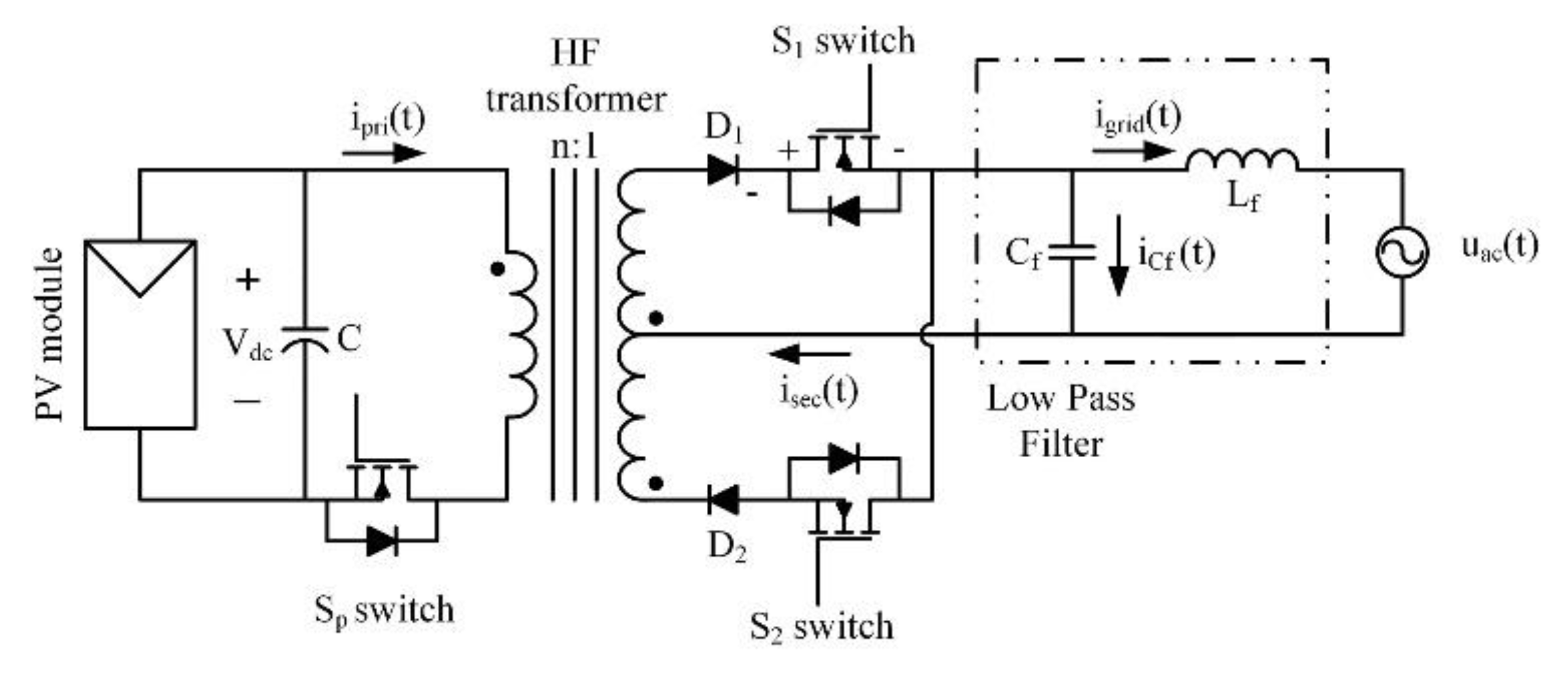
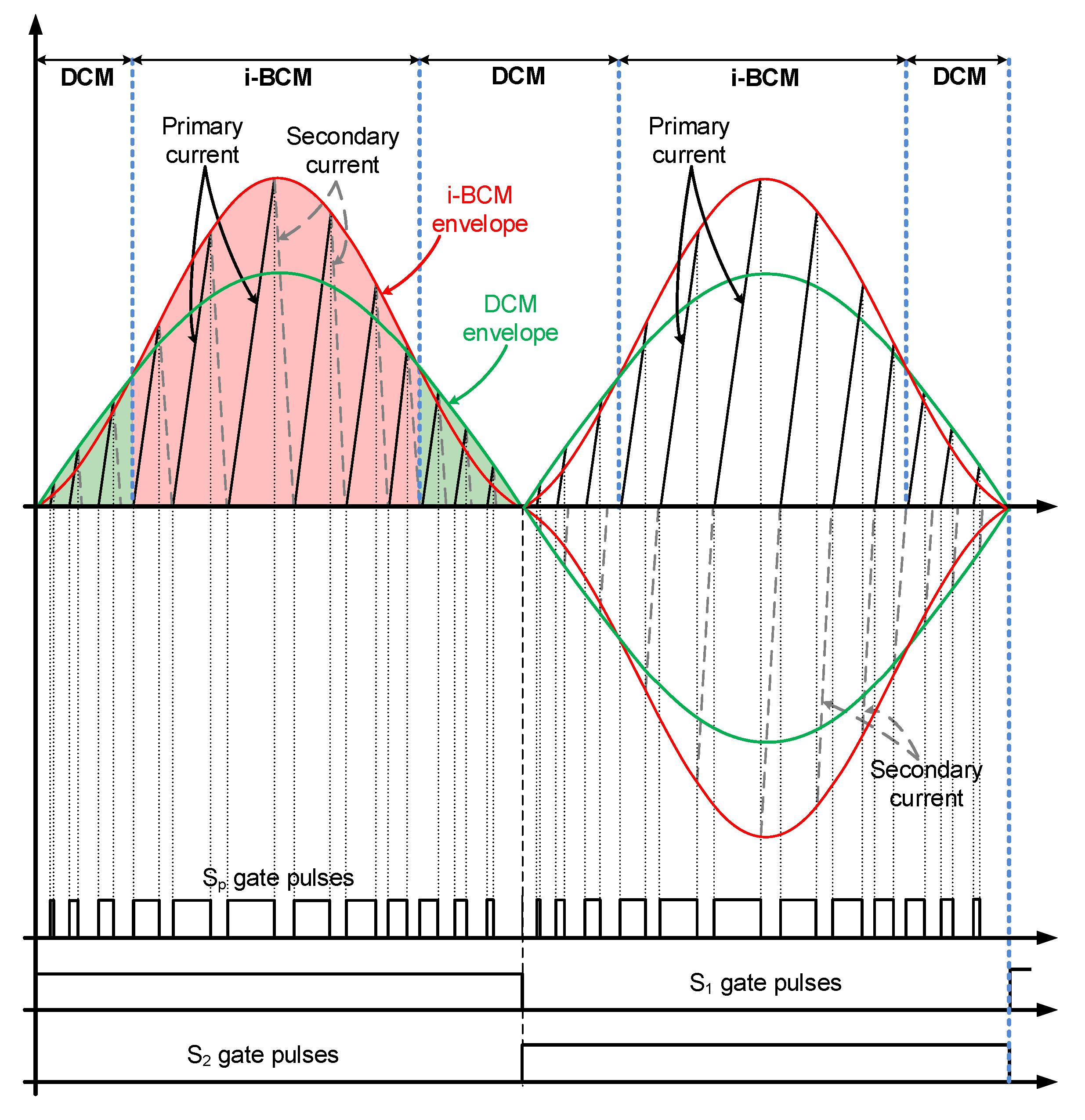
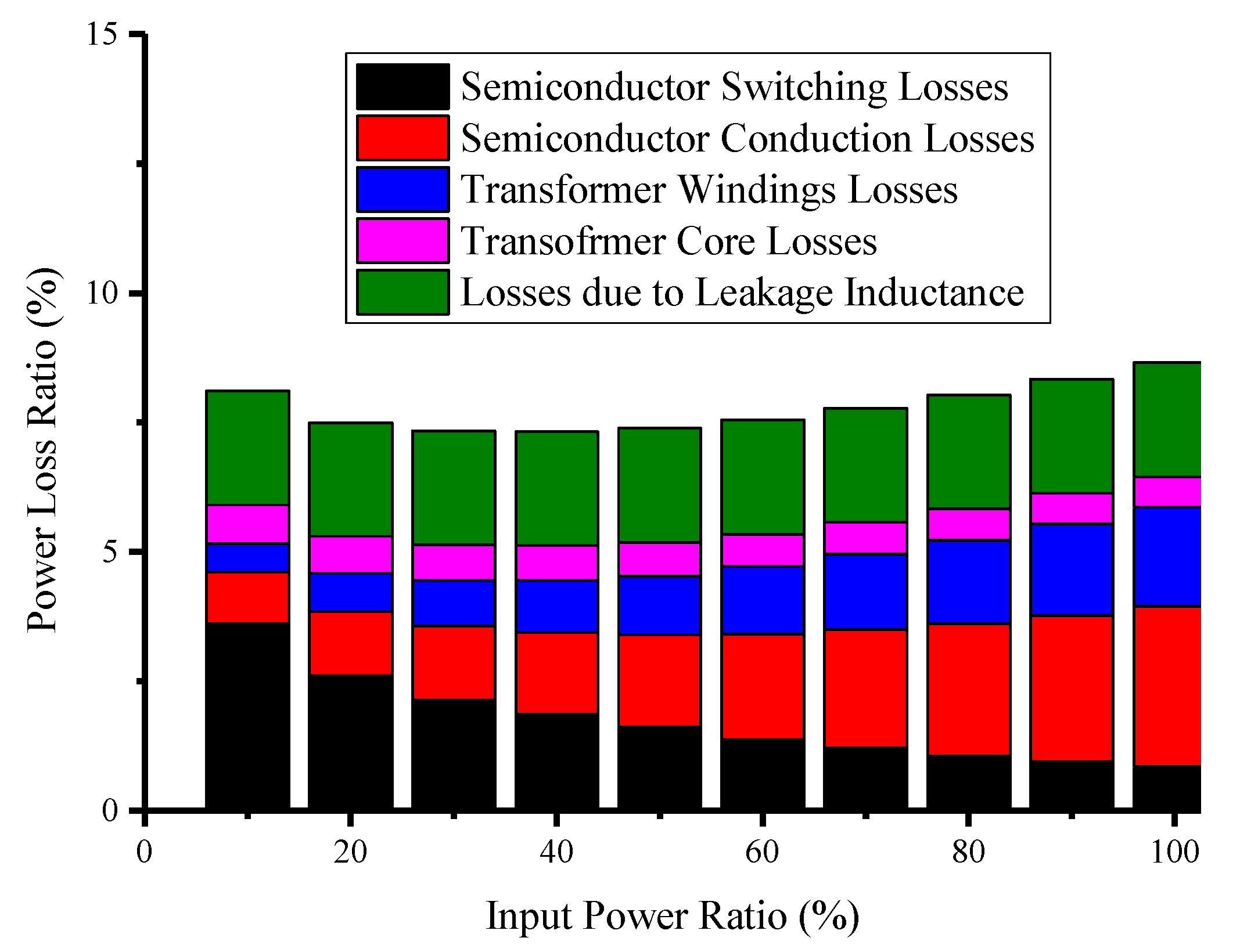
2. Power Losses in Hybrid DBCM

The converter power losses can be separated into two major categories: semiconductor losses and transformer losses. For the derivation of each component loss formulas, the rms or average values of the corresponding currents must be first analytically calculated. Equivalent mathematical formulations have been described for DCM and i-BCM in [14,18]. However, as will be shown in this section, due to the two different operating modes that exist within a sinusoidal wave half cycle, as well as because of the variable switching frequency imposed by the i-BCM operation during a segment of the sinusoidal wave, complex mathematical manipulations need to be carried out in order to derive precise equations for the DBCM operation during the full sinusoidal period.

2.1. Semiconductor Losses

Semiconductor losses can be further divided into conduction losses and switching losses. Firstly, for the main switch SP, since a power MOSFET is used, the conduction losses are:
P C L , S W , p r i = I p r i , r m s 2 R d s , p r i .
To calculate this value, the analytical expressions computed when the converter operates either fully in DCM or i-BCM are employed for the corresponding time intervals:
I p r i , r m s 2 = 1 π 0 π i p r i 2 ( t ) d ω t = 1 π ( 0 α i p r i 2 ( t ) d ω t + α π α i p r i 2 ( t ) d ω t + π α π i p r i 2 ( t ) d ω t ) = 1 π ( 2 0 α i p r i 2 ( t ) d ω t + α π α i p r i 2 ( t ) d ω t ) = I p r i , r m s , DCM 2 + I p r i , r m s , BCM 2 .
Next, a similar mathematical sequence as presented in [14] is employed, but instead of calculating the value for the complete sinusoidal cycle, it is now calculated only for the DCM segments of DBCM. Thus, it is deduced that:
I p r i , r m s , DCM 2 = V d c 2 d p 3 3 L 1 2 f s 2 2 m i = 1 α π m sin 3 ( π m i ) = V d c 2 d p 3 3 L 1 2 f s 2 1 4 m [ csc ( 3 π 2 m ) sin ( 3 π + m π 2 m ) + 3 csc ( π 2 m ) sin ( m π π 2 m ) + 3 csc ( π 2 m ) sin ( 2 α m + π m π 2 m ) csc ( 3 π 2 m ) sin ( 6 α m + 3 π m π 2 m ) ] .
Accordingly, for the i-BCM portion of the hybrid modulation, equivalent mathematical principles as shown in [18] are employed:
I p r i , r m s , BCM 2 = 1 3 ( V d c L 1 ) 2 ( t o n , p 1 + λ n ) 2 i = k 1 k 2 [ sin ω t i 1 ( sin ω t i 1 + λ n ) 3 ] i = k 1 k 2 ( λ n + sin ω t i 1 ) 2 = 1 3 ( V d c L 1 ) 2 ( t o n , p 1 + λ n ) 2 I p r i , r m s ( α ) ,
where ΣIpri,rms(α) is the generalized form of the trigonometric ratio calculated in [18], in the case that i-BCM occurs during a segment of the utility grid half cycle, meaning α < ωt < π − α, and its calculation is found in Appendix A.
Similarly, the conduction losses of the secondary windings’ switches S1, S2 are:
P C L , S W , sec = 2 I sec , r m s 2 R d s , sec .
To calculate the rms value of each of the transformer secondary side winding currents, an equivalent sequence as shown in Equations (2)–(4) is applied:
I s e c , r m s 2 = 1 2 π 0 2 π i sec 2 ( t ) d ω t = 1 2 π ( 0 α i sec 2 ( t ) d ω t + α π α i sec 2 ( t ) d ω t + π α π i sec 2 ( t ) d ω t ) = 1 2 π ( 2 0 α i sec 2 ( t ) d ω t + α π α i sec 2 ( t ) d ω t ) = I sec , r m s , DCM 2 + I sec , r m s , BCM 2
with:
I sec , r m s , DCM 2 = n V d c 2 d p 3 6 V a c p L 1 2 f s 2 2 m i = 1 α π m sin 2 ( π m i ) = n λ V d c d p 3 3 L 1 2 f s 2 1 4 π [ 2 α m + π + π csc ( π m ) sin ( π 2 α m m ) ]
and
I s e c , r m s , BCM 2 = 1 6 λ n ( n V d c L 1 ) 2 ( t o n , p 1 + λ n ) 2 i = k 1 k 2 [ sin 2 ω t i 1 ( sin ω t i 1 + λ n ) 3 ] i = k 1 k 2 ( λ n + sin ω t i 1 ) 2 I s e c , r m s , BCM 2 = 1 6 λ n ( n V d c L 1 ) 2 ( t o n , p 1 + λ n ) 2 I sec , r m s ( α ) ,
where ΣIsec,rms (α) is the generalized form of the trigonometric ratio calculated in [18], in the case that i-BCM occurs during a segment of the utility grid half cycle, meaning α < ωt < π − α, and its calculation is found in the Appendix A.
The conduction losses of the diodes D1, D2 are:
P C L , d = 2 I sec , a v g V d .
Assuming that the output current is purely sinusoidal and that the inverter supplies power under unitary power factor, then:
I sec , a v g = 1 2 π 0 π i sec ( t ) d ω t = 1 2 π 0 π I g r i d , p sin ( ω t ) d ω t = 2 π P P V V a c r m s .
Concerning the semiconductor switching losses, operation in DCM or i-BCM guarantees zero turn-ON losses for all the MOSFETs. The remaining turn-OFF losses of SP are calculated separately for the DCM and i-BCM segments during a grid half cycle, taking into consideration the operating period during each mode, and, as a result, the semiconductor switching losses are a function of the transition angle α as well:
P S L = P S L , DCM + P S L , BCM ,
with:
P S L , DCM = t f V d c d p 2 L 1 [ 2 V d c 2 m i = 1 α π m sin ( π m i ) + 2 n V d c λ 2 m i = 1 α π m sin 2 ( π m i ) ] = t f V d c d p 2 L 1 { V d c 2 m [ csc ( π 2 m ) sin ( m π π 2 m ) + csc ( π 2 m ) sin ( π m π + 2 α m 2 m ) ] + n V d c λ 1 π m [ π + 2 α m + π csc ( π m ) s i n ( π 2 α m m ) ] }
and
P S L , BCM = t f V d c 2 2 L 1 [ λ n i = k 1 k 2 sin ω t i 1 i = k 1 k 2 ( λ n + sin ω t i 1 ) 2 + 2 i = k 1 k 2 sin 2 ω t i 1 i = k 1 k 2 ( λ n + sin ω t i 1 ) 2 + n λ i = k 1 k 2 sin 3 ω t i 1 i = k 1 k 2 ( λ n + sin ω t i 1 ) 2 ] = t f V d c 2 2 L 1 P S L ( α )
where ΣPSL (α) is calculated in Appendix A.

2.2. Transformer Losses

The transformer losses can be separated into windings losses, core losses, and losses due to the energy dissipation stored on the leakage inductance (on the primary switch snubber).
Beginning with the windings, copper losses occur due the dc resistance of the windings, as well as due to the proximity and skin effect because of the high frequency current. To calculate the windings losses for the flyback inverter operating in DBCM, the semiempirical method presented in [24] is used, which calculates separately for each winding z the dc ohmic losses Pdc,z and the ac ohmic losses Pac,z, employing the analytical equations derived in the previous section:
P d c , z = I z , a v g 2 R d c , z ,
P a c , z = ( I z , r m s 2 I z , a v g 2 ) R d c , z F r , z .
To estimate the transformer core losses, the improved Generalized Steinmetz equation (iGSE) [25] is used, which is an empirical formula derived in order to apply the Steinmetz equation [26] for non-sinusoidal current waveforms, as is usually the case for power electronics converters. The transformer core losses for the flyback inverter operating in DBCM are calculated by summing the core loss during each switching cycle:
P C o r e = k f 2 π i = 0 k k f ( Δ Β i ) β i G S E α i G S E | d B i d t | α i G S E ( t i + 1 t i ) ,
where:
k f = k i G S E 2 β i G S E + 1 π α i G S E 1 ( 0 . 2761 + 1 . 7061 α i G S E + 1 . 354 ) .
Due to the complexity of the equations, which cannot be analytically solved because of the hybrid operation, approximated equations using curve fitting are derived using mathematical software [27] as a function of the transition angle α.
Finally, due to the leakage inductance of the transformer, an energy amount is not transferred from the primary to the secondary winding, but is dissipated in the form of heat on the primary switch snubber. The percentage of these power losses is equal to the percentage of the leakage inductance to the primary winding inductance.
The power losses described above occur under DBCM operation. As shown in [22], when the input power level drops under a critical power level (calculated based on the converter parameters), the flyback inverter operates entirely in DCM. For this case, the power losses equations are simplified, since only the DCM portion is considered for their analytical calculation.

3. Design Optimization Process for DBCM

Based on the power loss analysis for each component, it is now possible to appropriately select the flyback inverter parameters, i.e., transformer turns ratio and inductance, DCM switching frequency, and MOSFET breakdown voltage, for DBCM operation by employing a design methodology to achieve optimal converter performance. To achieve this, the numerical value that needs to be optimized (objective function) must be selected, as well as the constraints for the specific optimization problem.

3.1. Objective Function

As solar irradiance (and therefore, the PV panel output power) is not constant and varies considerably throughout the day, during the design process of a PV converter, instead of aiming for a high efficiency at nominal power, focus is given to achieve a maximum efficiency on various power levels. More specifically, the European (EU) weighted efficiency and the California Energy Commission (CEC) weighted efficiency methods were established in order to show the realistic performance of the power converter for different irradiance levels [28]. The weighting factors of the two methods for each power level are shown in Table 1. In this work, the European weighted efficiency was selected as the objective function, which is calculated based on the power loss formulas calculated for each converter component (1), (5), (9), (11), (14)–(16).
η = P o P i = 1 P L o s s e s P i ,
where:
P L o s s e s = P S i + P x f m r = ( P C L + P S W ) + ( P d c , 1 + P d c , 2 + P a c , 1 + P a c , 2 + P C o r e ) = ( P C L , p r i + P C L , sec + P C L , p r i + P S L + P C L , d ) + ( P d c , 1 + P d c , 2 + P a c , 1 + P a c , 2 + P C o r e )

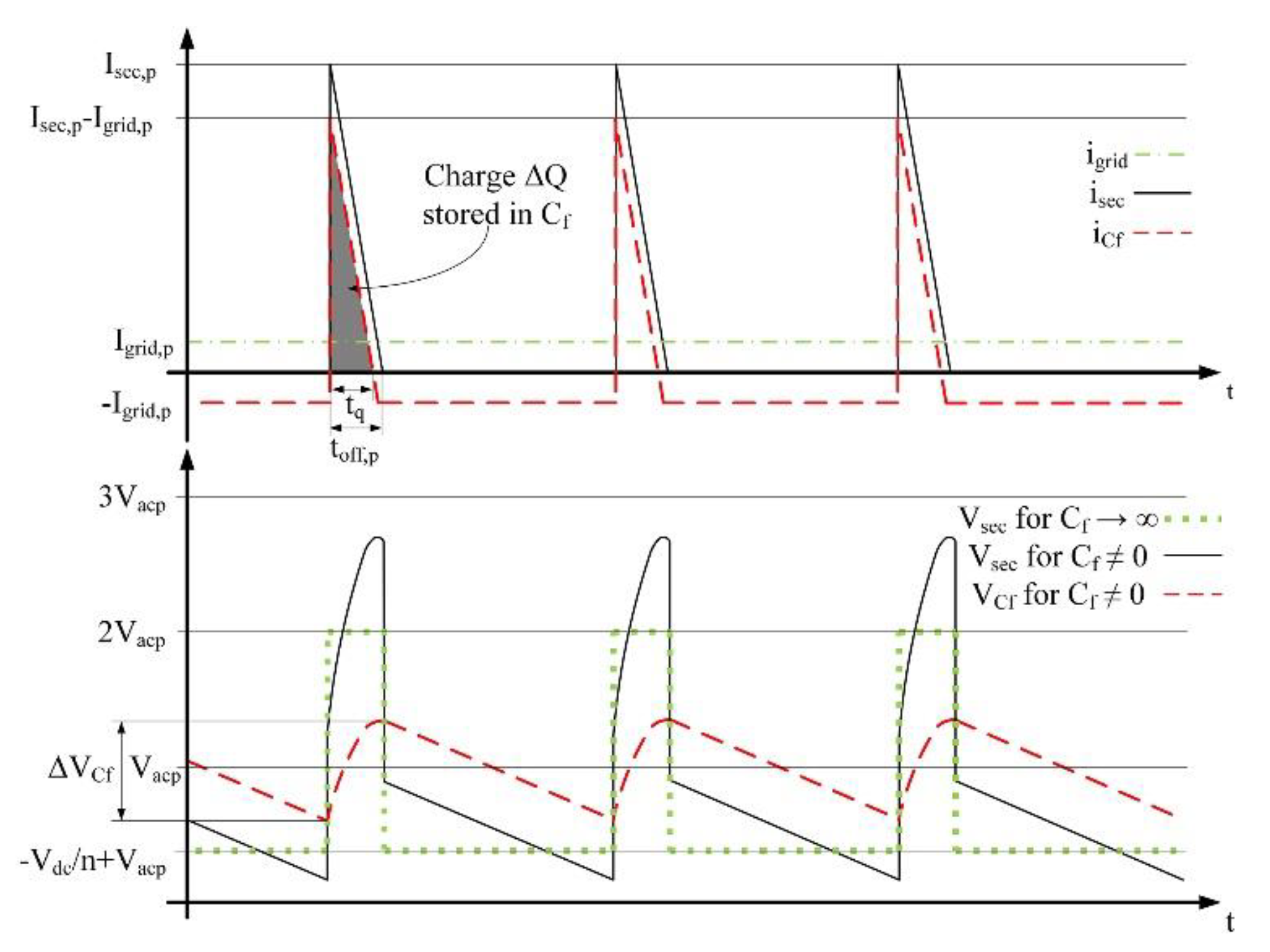
3.2. Design Constraints

The limitations on the design of a flyback microinverter can be again separated as limitations imposed by the semiconductor devices and limitations imposed by the transformer.
Concerning the transformer design, as with any magnetic component, two limitations must be met [29]:
  • The core peak flux density (which for the case of the flyback microinverter operated in DBCM is for ωt = π/2 at maximum input power) must be lower than the ferrite material maximum flux density to avoid core saturation.
  • The window utilization factor for the given core type, which is the ratio of the area of all the transformer windings to the transformer window, must be lower or equal to the maximum permitted value (for the windings to fit).
Regarding the semiconductor devices, the voltage induced during each switching cycle must be lower than the breakdown voltage of the selected switches. However, by arbitrarily selecting a power MOSFET with a high breakdown voltage, its higher ON resistance (caused by the longer epitaxial layer) will limit the maximum converter efficiency due to the increased conduction losses. What is more, the maximum voltage induced on each switch is a function of the inverter design parameters (i.e., transformer turns ratio), and therefore, its accurate determination is essential for the selection of the design parameters through the optimization process. During this calculation, it is essential to include the effect of the output filter capacitor value, as will be shown below.
More specifically, assuming that the high frequency voltage fluctuation across the filter capacitor Cf, shown in Figure 1, is negligible, then the peak voltage for each switch will be observed at the maximum grid voltage (ωt = π/2):
V p r i = V d c + n V C f Δ V C f 0 V p r i , p = V d c + n V a c p ,
V sec = 2 V C f Δ V C f 0 V sec , p = 2 V a c p .
However, this implies that a large capacitor value would be used for the output filter, which would lower the converter power density and, more importantly, increase the phase difference between the grid voltage and the converter output current, lowering the inverter power factor. This is not acceptable for a grid-connected PV inverter and, thus, the capacitance value must be appropriately selected. In Figure 3, where the current and voltage waveforms on the transformer secondary side are shown, the increase of the maximum voltage on the transformer secondary side switch due to the capacitor voltage fluctuation can be observed. This voltage fluctuation is transferred to SP as well. To determine the maximum ΔVCf, the charge ΔQ is first calculated for the switching cycle near ωt = π/2:
Δ Q = 0 t q i C f ( t )   d t = 0 t q ( i sec ( t ) I g r i d , p )   d t = 1 2 ( I sec , p I g r i d , p ) t q .
Using Thales’ theorem for similar triangles, it is deduced that:
t q t o f f , p = I sec , p I g r i d , p I sec , p t q = I sec , p I g r i d , p I sec , p t o f f , p .
Thus, the capacitor fluctuation is calculated using (22) and (23):
Δ V C f = 1 C f Δ Q = 1 C f 1 2 ( I sec , p I g r i d , p ) 2 I sec , p t o f f , p .
The maximum capacitor fluctuation will occur under nominal converter output power at ωt = π/2. Therefore, as shown in Figure 2, the converter will operate in the i-BCM segment, and the i-BCM equations should be employed [18], which, after some mathematical manipulations, leads to:
Δ V C f = 1 C f 1 2 ( n V d c L 1 t o n , p 2 P P V , n o m V a c p ) 2 n V d c L 1 t o n , p λ n 1 + λ n t o n , p ( 1 + λ n ) = 1 C f ( 4 f s , a v g L 1 P P V , n o m π + V d c ( π V d c + 2 n V a c p ) ) 2 2 f s , a v g 2 L 1 n 2 π 2 V a c p 3 .
Finally, taking into account the voltage fluctuation of the capacitor, the constraints for the selection of the semiconductor switches are:
V p r i , p = V d c + n V C f , p = V d c + n ( V a c p + Δ V C f 2 ) ,
V s e c , p = 2 V C f , p = 2 ( V a c p + Δ V C f 2 ) = 2 V a c p + Δ V C f .

3.3. Optimization Sequence

The flowchart of the optimization process is shown in Figure 4. Having analytically obtained the efficiency equation for the microinverter operating in hybrid DBCM (objective function), a global maximum can be determined by recursively selecting different values for the design independent variables. Those variables are the design values that determine the characteristics of each converter instance implementation and are: the transformer turns ratio n, the switching frequency when the converter operates in DCM f, the peak ON time at nominal power ton,p,max, the transformer windings current density J, and the transformer ferrite core maximum operational magnetic flux density Bp. As noted in the section above, these independent variables are affected by the design constraints, e.g., a winding with a very low current density (i.e., many litz wire strands) will not fit in the given transformer utilization window. For each feasible combination of the independent variables, the expected weighted efficiency of this design is calculated using (18) with the weights of Table 1. This sequence is repeated for multiple combinations until a global maximum is found. As this is an off-line method (i.e., the optimization algorithm is applied during the design phase and not during the operation phase), the differential evolution stochastic method for constrained nonlinear global optimization is used through a software platform [27]. This optimization method is compute intensive, but provides a global maximum. For the design that achieves the maximum weighted efficiency, the rest of the parameters are calculated and presented to the designer in order to select the remaining component values [22]. Finally, the control parameters are also calculated to be input to the microcontroller program. An example of the application of this algorithm is shown in the following section, where the theoretical analysis (loss equations derived above) will be compared to experimental results for a given design.

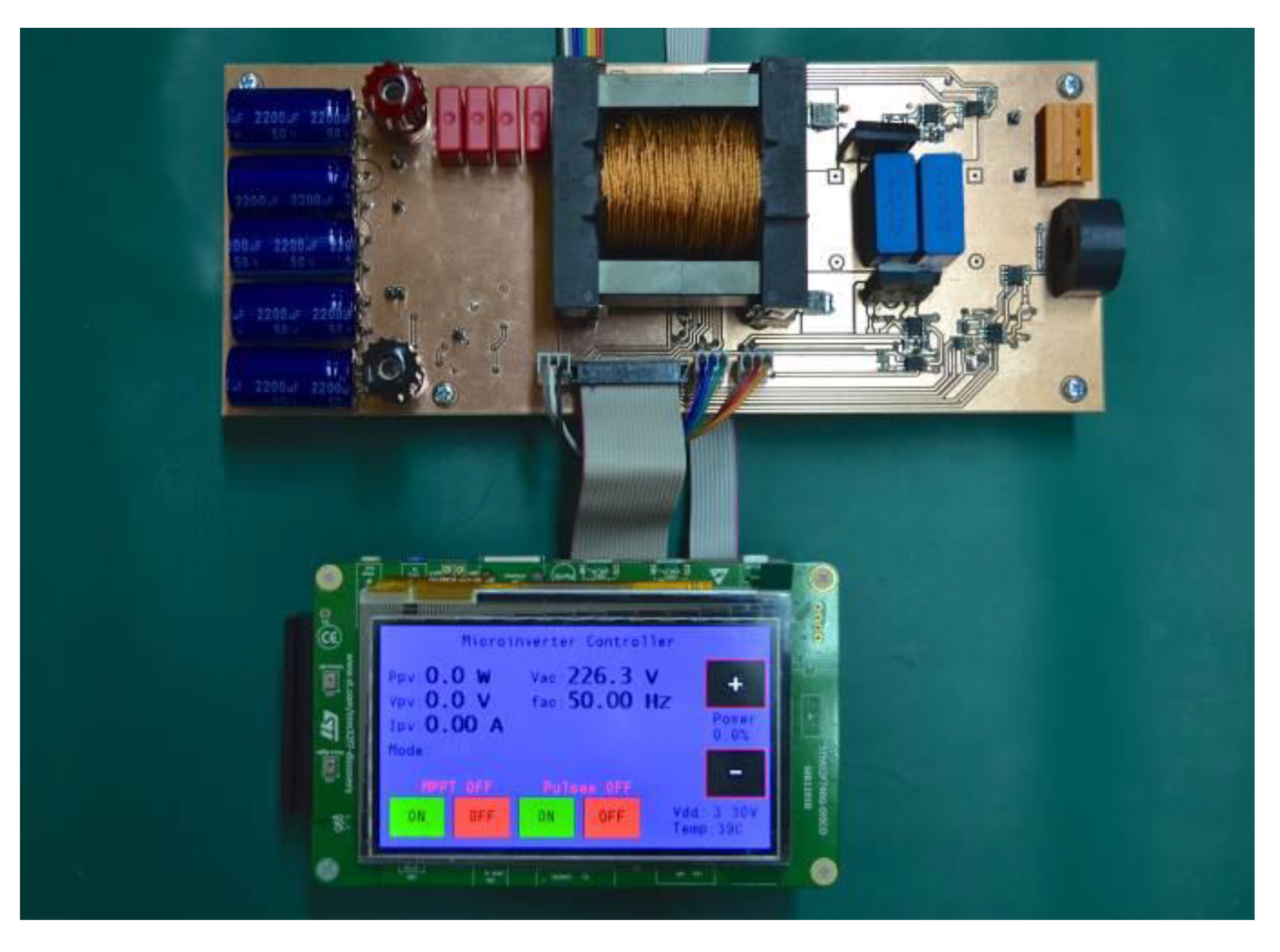
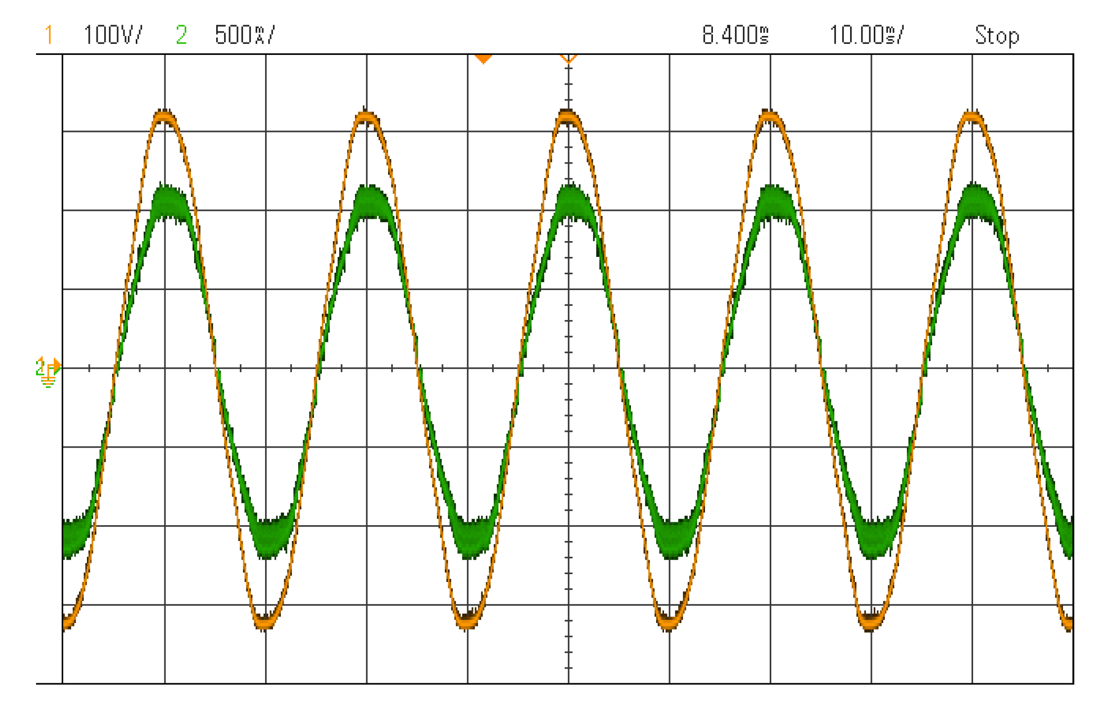
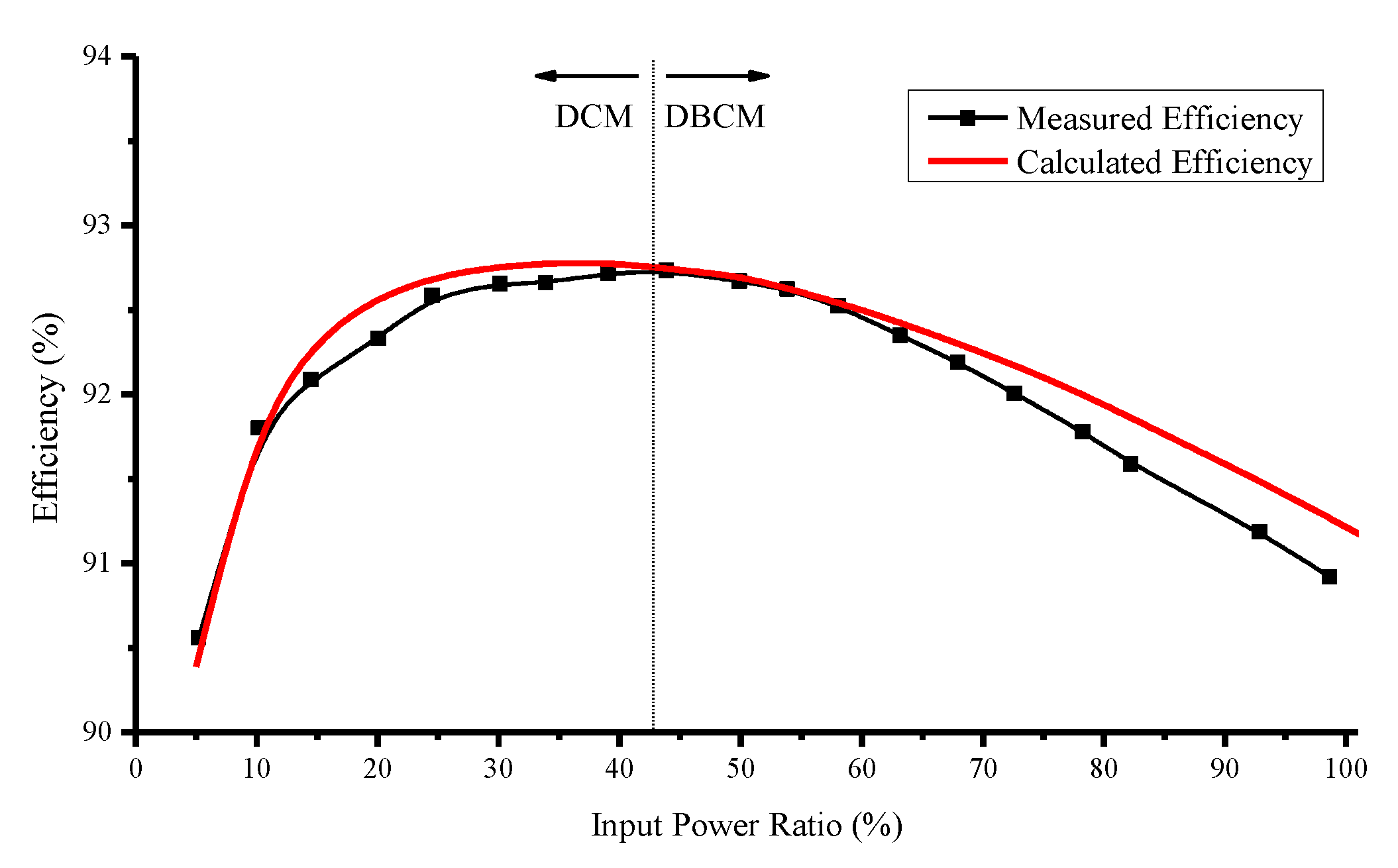
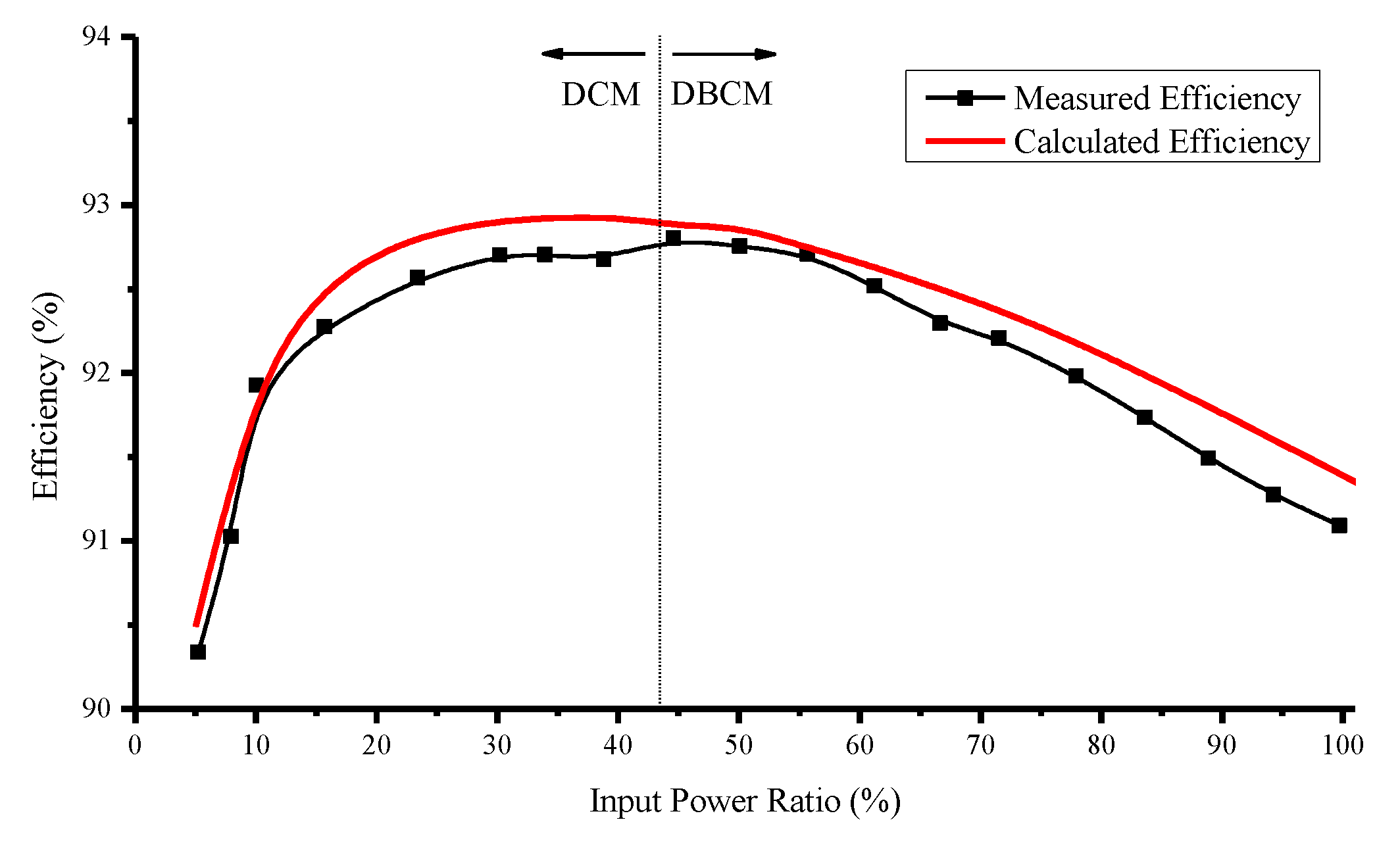
4. Optimization Algorithm Verification

To verify the optimization process as well as the power loss analysis, a laboratory experimental prototype was built (shown in Figure 5), with the component values, outlined in Table 2, selected by the algorithm. The flyback inverter was designed to be powered by a monocrystalline 72-cell panel with a nominal power of 180 W at 36 V (at STC). The panel operating temperature limits were selected to be 0 °C and 60 °C. Therefore, the optimization process was carried out for the worst case, which, for a PV system, is the minimum temperature (resulting to the highest input power).
The flyback inverter is controlled by the STM32F746 microcontroller, which samples the converter input and output voltage and determines the modulation of SP according to the hybrid DBCM formulas. The optimal operation values (i.e., DCM switching frequency, maximum pulse length) are calculated offline and entered as parameters, together with the converter component values. Figure 6 shows the inverter output current at maximum power.
Efficiency measurements for different input voltages (corresponding to different PV panel temperature) and power levels were carried out using the precision power analyzer LMG500 of ZES Zimmer manufacturer in order to determine the weighted efficiency of the prototype as well as to validate the power loss analysis for the DBCM modulation. The measured efficiency as a function of the input power compared to the calculated one, based on the power loss analysis, is shown in Figure 7, Figure 8 and Figure 9, for different input voltages.
The convergence between the theoretical and experimental results validates the power loss analysis as well as the optimization process. As can be observed, the component values are appropriately selected by the algorithm in order to have the maximum efficiency between 20% and 50% of the nominal input power, where the weights of the European efficiency are more significant. This is true for all three input voltage values. Since the optimization algorithm was carried out for the worst case (minimum temperature and maximum input voltage and power), the converter efficiency for the other cases (STC/36 V and 60 °C/31 V) is slightly improved.
The calculated and measured European efficiencies are shown in Table 3. As a comparison, the calculated European efficiency for a converter with the same specifications optimally designed for i-BCM operation [18] is also shown in this table. The achieved weighted efficiency is always higher than the one of the converter operating in pure i-BCM, underlining the performance benefit of the flyback inverter designed for DBCM operation.
Having validated the power loss analysis, it is possible to break down the power losses of each of the components as a function of the input power level (shown in Figure 10). As the input power increases, the percentage of the semiconductor switching losses decreases, whereas the rest of the component losses increase. As a result, the optimization algorithm appropriately selects the component parameters to achieve the global minimum of the total losses near the 50% mark of the nominal power, achieving the highest weighted efficiency.

5. Conclusions

The characteristics of the flyback current source inverter qualify it to be used as a single-stage converter in photovoltaic modules. Operation in DBCM combines the advantages of both DCM and i-BCM (lower switching and conduction losses and higher energy density). In this work, a fully parameterized power loss model of the converter for the DBCM modulation was analyzed and implemented. This was made possible by generating the equations that describe the average and rms current values of all the converter key components for operation in DBCM. Moreover, it then led to the formulation of an optimization algorithm in order to determine the design values based on the converter specifications, so as to achieve the maximum weighted efficiency. Experimental results validated this analysis and also showed the increased performance compared to a flyback inverter with the same specifications optimized for operation exclusively in i-BCM.
The generation of the analytical equations that describe the operation of each component of the flyback micro-inverter allows the designer to appropriately select the design values based on the application specifications (e.g., power and voltage range), as well as other technical or non-technical constraints (e.g., component cost, availability, packaging). Through the power loss analysis, the effect of each component on the total performance of the converter can also be predicted, leading to a better cooling design. The mathematical manipulations presented in this paper can be applied to other inverters with similar hybrid switching strategies.

Author Contributions

Conceptualization, G.C., A.N. and E.T.; methodology, G.C. and A.N.; software, G.C.; validation, G.C.; formal analysis, G.C., A.N. and E.T.; investigation, G.C., A.N. and E.T.; resources, G.C. and A.N.; data curation, G.C.; writing—original draft preparation, G.C.; writing—review and editing, A.N. and E.T.; visualization, G.C. and A.N.; supervision, E.T.; funding acquisition, E.T. All authors have read and agreed to the published version of the manuscript.

Funding

This research received no external funding.

Institutional Review Board Statement

Not applicable.

Informed Consent Statement

Not applicable.

Conflicts of Interest

The authors declare no conflict of interest. The funders had no role in the design of the study; in the collection, analyses, or interpretation of data; in the writing of the manuscript, or in the decision to publish the results.

Nomenclature

PCL,SW,priConduction losses of the primary switch (W).
Ipri,rmsRMS current value of the primary transformer side (A).
Rds,priON-resistance of the primary switch (Ω).
ipriInstant current value of the primary transformer side (A).
Ipri,rms,DCMRMS current value of the primary transformer side during the DCM segment of DBCM (A).
Ipri,rms,BCMRMS current value of the primary transformer side during the i-BCM segment of DBCM (A).
VdcInput voltage (V).
L1Transformer primary winding inductance (H).
dpPeak duty cycle when in DCM.
fsDCM switching frequency (Hz).
mRatio of the utility grid half cycle period to the DCM switching period.
ton,pPeak ON-time of the primary side switch when in i-BCM (s).
ton,p,maxton,p at nominal power (s).
kNumber of switching cycles during a utility grid half cycle for DBCM operation.
k1Νumber of switching cycles until ωt = α.
k2Number of switching cycles until ωt = π − α.
λRatio of the input voltage to the peak grid voltage.
nTransformer turns ratio.
αTransition angle between DCM and BCM (rad).
PCL,SW,secConduction losses of the secondary switches (W).
Isec,rmsRMS current value of each of the secondary transformer side windings (A).
Rdc,secON-resistance of the secondary switches (Ω).
Isec,rms,DCMRMS current value of each of the secondary transformer side windings during the DCM segment of DBCM (A).
Isec,rms,BCMRMS current value of each of the secondary transformer side windings during the i-BCM segment of DBCM (A).
PCL,dConduction losses of the diodes (W).
Isec,avgAverage current value of each of the transformer secondary side windings current (A).
VdDiode forward voltage (V).
isecInstant current value of the secondary transformer side (A).
PPVInverter input power (W).
PPV,nomMaximum inverter input power (W).
uacInstant voltage value of the utility grid (V).
VacrmsRMS voltage value of the utility grid (V).
PSLSemiconductor switching losses (W).
PSL,DCMSemiconductor switching losses for the DCM segment of DBCM (W).
PSL,BCMSemiconductor switching losses for the i-BCM segment of DBCM (W).
tfCurrent fall time of the primary switch (s).
Pdc,zDC copper losses of the winding z (W).
Pac,zAC copper losses of the winding z (W).
Iz,avgAverage current value of the winding z (A).
Iz,rmsRMS current value of the winding z (A).
Fr,zResistance factor of the winding z.
PCoreTransformer core losses (W).
ΔBiFlux swing during each switching cycle i (T).
αiGSE,βiGSE, kiGSEParameters of the Steinmetz equation loss formula.
BiTransformer core magnetic flux density at time ti (Τ).
ηConverter efficiency at a given power level.
PiConverter input power at a given power level (W).
PoConverter output power at a given power level (W).
PLossesConverter losses at a given power level (W).
PSiConverter semiconductor losses at a given power level (W).
PxfmrConverter transformer losses at a givern power level (W).
PCLConverter semiconductor conduction losses at a given power level (W)
PSWConverter semiconductor switching losses at a given power level (W).
VpriVoltage of the primary switch when in OFF state (V).
Vpri,pMaximum value of Vpri (V).
VsecVoltage of each secondary switch when in OFF state (V).
Vsec,pMaximum value of Vsec (V).
toff,pOFF-time of the primary switch at ωt = π/2 (s).
VacpUtility grid voltage value at ωt = π/2 (V).
Ipri,pPeak current value of the primary transformer side at ωt = π/2 (A).
Isec,pPeak current value of the secondary transformer side at ωt = π/2 (A).
ΔVCfVoltage fluctuation of filter capacitor (V).
tqTime segment during which the filter capacitor is charged at ωt = π/2 (s).
igridInstant value of the converter current supplied to the grid (A).
Igrid,pValue of the converter current supplied to the grid at ωt = π/2 (A).
iCfInstant current value of the filter capacitor (A).
fs,avgAverage converter switching frequency (Hz).
JCurrent density of the transformer windings (A/mm2).
BpMaximum operational flux density (T).

Appendix A

To calculate the various trigonometric ratios needed to derive the power losses of the flyback inverter operating in DBCM, the following ratios must first be calculated:
Σ 1 p ( λ n ) = i = 0 w sin p θ i 1 i = 0 w ( λ n + sin θ i 1 ) ,
Σ 2 p ( λ n ) = i = 0 w sin p θ i 1 i = 0 w ( λ n + sin θ i 1 ) 2 ,
which can be transformed into the following integrals, as it can be proven by any mathematical software:
Σ 1 p ( λ n ) 1 φ 0 φ sin p θ ( λ n + sin θ )   d θ = S 1 p ( λ n , φ ) ,
Σ 2 p ( λ n ) 1 φ 0 φ sin p θ ( λ n + sin θ ) 2   d θ = S 2 p ( λ n , φ ) ,
where φ is the transition angle between DCM and i-BCM.
Beginning with the fundamental S10 [30]:
S 1 0 ( λ n , φ ) = 1 φ 1 1 ( λ n ) 2 [ ln ( 1 + 1 1 ( λ n ) 2 λ n tan ( φ 2 ) 1 + 1 + 1 ( λ n ) 2 λ n tan ( φ 2 ) ) ln ( 1 1 ( λ n ) 2 1 + 1 ( λ n ) 2 ) ] , f o r   0 < λ n < 1
S 1 0 ( λ n , φ ) = 1 φ [ tan ( π 4 φ 2 ) 1 ] , f o r   λ n = 1
S 1 0 ( λ n , φ ) = 1 φ 1 ( λ n ) 2 1 arctan [ λ n tan ( φ 2 ) ( λ n ) 2 1 ] , f o r   λ n > 1
Accordingly, for S20 [30]:
S 2 0 ( λ n , φ ) = 1 ( λ n ) 2 1 ( 1 φ [ cos θ λ n + sin θ ] 0 φ + 1 φ 0 φ λ n λ n + sin θ d θ ) = 1 ( λ n ) 2 1 ( 1 φ cos φ λ n + sin φ n λ + λ n S 1 0 ( λ n , φ ) ) , f o r   λ n 1
S 2 0 ( λ n , φ ) = 1 φ [ 1 2 tan ( π 4 φ 2 ) + 1 2 tan 3 ( π 4 φ 2 ) 1 3 ] , f o r   λ n = 1 ,
The remaining ratios needed can be calculated based on the fundamental ones:
S 1 1 ( λ n , φ ) = 1 S 1 0 ( λ n , φ ) ,
S 1 2 ( λ n , φ ) = λ n + 1 φ ( 1 cos φ ) + ( λ n ) 2 S 1 0 ( λ n , φ ) ,
S 1 3 ( λ n , φ ) = ( λ n ) 2 λ n 1 φ ( 1 cos φ ) + 1 φ [ φ 2 sin ( 2 φ ) 4 ] ( λ n ) 3 S 1 0 ( λ n , φ ) ,
S 1 4 ( λ n , φ ) = ( λ n ) 3 + ( λ n ) 2 1 φ ( 1 cos φ ) + λ n 1 φ [ φ 2 sin ( 2 φ ) 4 ] + 1 φ ( cos φ + cos 3 φ 3 + 2 3 ) + ( λ n ) 4 S 1 0 ( λ n , φ )
S 1 5 ( λ n , φ ) = ( λ n ) 4 + ( λ n ) 3 1 φ ( 1 cos φ ) + ( λ n ) 2 1 φ [ φ 2 sin ( 2 φ ) 4 ] λ n 1 φ [ 3 cos φ 4 + 1 12 cos ( 3 φ ) + 2 3 ] + 1 φ [ 3 φ 8 1 4 sin ( 2 φ ) + 1 32 sin ( 4 φ ) ] ( λ n ) 5 S 1 0 ( λ n , φ )
S 2 1 ( λ n , φ ) = S 1 0 ( λ n , φ ) λ n S 2 0 ( λ n , φ ) ,
S 2 2 ( λ n , φ ) = λ n S 1 0 ( λ n , φ ) + S 1 1 ( λ n , φ ) + ( λ n ) 2 S 2 0 ( λ n , φ ) ,
S 2 3 ( λ n , φ ) = ( λ n ) 2 S 1 0 ( λ n , φ ) λ n S 1 1 ( λ n , φ ) + S 1 2 ( λ n , φ ) ( λ n ) 3 S 2 0 ( λ n , φ ) ,
S 2 4 ( λ n , φ ) = ( λ n ) 3 S 1 0 ( λ n , φ ) + ( λ n ) 2 S 1 1 ( λ n , φ ) λ n S 1 2 ( λ n , φ ) + ( λ n ) 4 S 2 0 ( λ n , φ ) ,
S 2 5 ( λ n , φ ) = ( λ n ) 4 S 1 0 ( λ n , φ ) ( λ n ) 3 S 1 0 ( λ n , φ ) + ( λ n ) 2 S 1 2 ( λ n , φ ) λ n S 1 3 ( λ n , φ ) + S 1 4 ( λ n , φ ) ( λ n ) 5 S 2 0 ( λ n , φ )
S 2 6 ( λ n , φ ) = ( λ n ) 5 S 1 0 ( λ n , φ ) + ( λ n ) 4 S 1 1 ( λ n , φ ) ( λ n ) 3 S 1 2 ( λ n , φ ) + ( λ n ) 2 S 1 3 ( λ n , φ ) λ n S 1 4 ( λ n , φ ) + S 1 5 ( λ n , φ ) + ( λ n ) 6 S 2 0 ( λ n , φ )
As all of the basic trigonometric ratios needed have been calculated, the ratios for the power loss analysis can now be derived.
Because of the variable switching frequency of i-BCM, the calculation of each switching cycle period is recursive, making the determination of this trigonometric ratio extremely complicated. To overcome this problem, ΣIpri,rms(α) is instead calculated as the difference between operation in pure i-BCM (0 < ωt < π), minus a segment of i-BCM operation during 0 < ωt < α, which can be more easily calculated.
I p r i , r m s ( α ) = i = 0 k [ sin ω t i 1 ( sin ω t i 1 + λ n ) ] 3 i = 0 k ( λ n + sin ω t i 1 ) 2 2 α π i = 0 k 1 [ sin ω t i 1 ( sin ω t i 1 + λ n ) ] 3 i = 0 k 1 ( λ n + sin ω t i 1 ) 2 = [ 3 8 + 4 3 π ( λ n ) ] 2 α π ( λ n ) 3 i = 0 k 1 sin 3 ω t i 1 + 3 ( λ n ) 2 i = 0 k 1 sin 4 ω t i 1 + 3 ( λ n ) i = 0 k 1 sin 5 ω t i 1 + i = 0 k 1 sin 6 ω t i 1 i = 0 k 1 ( λ n + sin ω t i 1 ) 2 = [ 3 8 + 4 3 π ( λ n ) ] 2 α π [ ( λ n ) 3 S 2 3 ( λ n , α ) + 3 ( λ n ) 2 S 2 4 ( λ n , α ) + 3 ( λ n ) S 2 5 ( λ n , α ) + S 2 6 ( λ n , α ) ]
Accordingly, using the equivalent mathematical manipulations as presented above:
I sec , r m s ( α ) = i = 0 k [ sin 2 ω t i 1 ( sin ω t i 1 + λ n ) 3 ] i = 0 k ( λ n + sin ω t i 1 ) 2 2 α π i = 0 k 1 [ sin 2 ω t i 1 ( sin ω t i 1 + λ n ) 3 ] i = 0 k 1 ( λ n + sin ω t i 1 ) 2 = [ 4 3 π + ( λ 2 n ) ] 2 α π ( λ n ) 3 i = 0 k 1 sin 2 ω t i 1 + 3 ( λ n ) 2 i = 0 k 1 sin 3 ω t i 1 + 3 ( λ n ) i = 0 k 1 sin 4 ω t i 1 + i = 0 k 1 sin 5 ω t i 1 i = 0 k 1 ( λ n + sin ω t i 1 ) 2 = [ 4 3 π + ( λ 2 n ) ] 2 α π [ ( λ n ) 3 S 2 2 ( λ n , α ) + 3 ( λ n ) 2 S 2 3 ( λ n , α ) + 3 ( λ n ) S 2 4 ( λ n , α ) + S 2 5 ( λ n , α ) ]
P S L [ λ n i = 0 k sin ω t i 1 i = 0 k ( λ n + sin ω t i 1 ) 2 + 2 i = 0 k sin 2 ω t i 1 i = 0 k ( λ n + sin ω t i 1 ) 2 + n λ i = 0 k sin 3 ω t i 1 i = 0 k ( λ n + sin ω t i 1 ) 2 ] 2 α π [ λ n i = 0 k 1 sin ω t i 1 i = 0 k 1 ( λ n + sin ω t i 1 ) 2 + 2 i = 0 k 1 sin 2 ω t i 1 i = 0 k 1 ( λ n + sin ω t i 1 ) 2 + n λ i = 0 k 1 sin 3 ω t i 1 i = 0 k 1 ( λ n + sin ω t i 1 ) 2 ] = ( 2 n λ π ) 2 α π [ λ n i = 0 k 1 sin ω t i 1 i = 0 k 1 ( λ n + sin ω t i 1 ) 2 + 2 i = 0 k 1 sin 2 ω t i 1 i = 0 k 1 ( λ n + sin ω t i 1 ) 2 + n λ i = 0 k 1 sin 3 ω t i 1 i = 0 k 1 ( λ n + sin ω t i 1 ) 2 ] = ( 2 n λ π ) 2 α π [ ( λ n ) S 2 1 ( λ n , α ) + S 2 2 ( λ n , α ) + ( n λ ) S 2 3 ( λ n , α ) ]

References

  1. Liu, B.; Duan, S.; Cai, T. Photovoltaic DC-building-module-based BIPV system—Concept and design considerations. IEEE Trans. Power Electron. 2011, 26, 1418–1429. [Google Scholar] [CrossRef]
  2. Leuenberger, D.; Biela, J. PV-module-integrated AC inverters (AC modules) with subpanel MPP tracking. IEEE Trans. Power Electron. 2017, 32, 6105–6118. [Google Scholar] [CrossRef]
  3. Voglitsis, D.; Papanikolaou, N.; Kyritsis, A. Incorporation of harmonic injection in an interleaved flyback inverter for the implementation of an active anti-islanding technique. IEEE Trans. Power Electron. 2017, 32, 8526–8543. [Google Scholar] [CrossRef]
  4. Kjaer, S.B.; Pedersen, J.K.; Blaabjerg, F. A review of single-phase grid-connected inverters for photovoltaic modules. IEEE Trans. Ind. Appl. 2005, 41, 1292–1306. [Google Scholar] [CrossRef]
  5. Quan, L.; Wolfs, P. A review of the single phase photovoltaic module integrated converter topologies with three dc link con-figurations. IEEE Trans. Power Electron. 2008, 23, 1320–1333. [Google Scholar] [CrossRef] [Green Version]
  6. Meneses, D.; Blaabjerg, F.; García, Ó.; Cobos, J.A. Review and comparison of step-up transformerless topologies for photovoltaic AC-module application. IEEE Trans. Power Electron. 2013, 28, 2649–2663. [Google Scholar] [CrossRef] [Green Version]
  7. Freddy, T.K.S.; Rahim, N.A.; Hew, W.-P.; Che, H.S. Comparison and analysis of single-phase transformerless grid-connected PV inverters. IEEE Trans. Power Electron. 2014, 29, 5358–5369. [Google Scholar] [CrossRef]
  8. Feng, X.; Wang, F.; Wu, C.; Luo, J.; Zhang, L. Modeling and comparisons of aggregated flyback microinverters in aspect of harmonic resonances with the grid. IEEE Trans. Ind. Electron. 2019, 66, 276–285. [Google Scholar] [CrossRef]
  9. Chen, M.; Zheng, R.; Fu, Y.; Qi, J.; Han, F.; Jiang, F.; Yao, W. An analog control strategy with multiplier-less power calcu-lation circuit for flyback microinverter. IEEE Trans. Power Electron. 2021, 36, 8617–8621. [Google Scholar] [CrossRef]
  10. Falconar, N.; Beyragh, D.S.; Pahlevani, M. An adaptive sensorless control technique for a flyback-type solar tile microin-verter. IEEE Trans. Power Electron. 2020, 35, 13554–13562. [Google Scholar] [CrossRef]
  11. Hasan, R.; Hassan, W.; Xiao, W. PV microinverter solution for high voltage gain and soft switching. IEEE Trans. Emerg. Sel. Top. Power Electron. 2021, in press. Available online: https://ieeexplore.ieee.org/document/9362130 (accessed on 28 October 2021). [CrossRef]
  12. Kyritsis, A.; Tatakis, E.C.; Papanikolaou, N. Optimum design of the current-source flyback inverter for decentralized grid-connected photovoltaic systems. IEEE Trans. Energy Convers. 2008, 23, 281–293. [Google Scholar] [CrossRef]
  13. Zhang, Z.; He, X.-F.; Liu, Y.-F. An optimal control method for photovoltaic grid-tied-interleaved flyback microinverters to achieve high efficiency in wide load range. IEEE Trans. Power Electron. 2013, 28, 5074–5087. [Google Scholar] [CrossRef]
  14. Nanakos, A.C.; Tatakis, E.C.; Papanikolaou, N.P. A weighted-efficiency-oriented design methodology of flyback inverter for ac photovoltaic modules. IEEE Trans. Power Electron. 2012, 27, 3221–3233. [Google Scholar] [CrossRef]
  15. Hu, H.; Harb, S.; Kutkut, N.H.; Shen, Z.J.; Batarseh, I. A single-stage microinverter without using eletrolytic capacitors. IEEE Trans. Power Electron. 2013, 28, 2677–2687. [Google Scholar] [CrossRef]
  16. Zengin, S.; Deveci, F.; Boztepe, M. Decoupling capacitor selection in DCM flyback PV microinverters considering harmonic distortion. IEEE Trans. Power Electron. 2012, 28, 816–825. [Google Scholar] [CrossRef]
  17. Gao, M.; Chen, M.; Zhang, C.; Qian, Z. Analysis and implementation of an improved flyback inverter for photovoltaic AC module applications. IEEE Trans. Power Electron. 2013, 29, 3428–3444. [Google Scholar] [CrossRef]
  18. Nanakos, A.C.; Christidis, G.C.; Tatakis, E.C. Weighted efficiency optimization of flyback micro-inverter under improved boundary conduction mode (i-BCM). IEEE Trans. Power Electron. 2015, 30, 5548–5564. [Google Scholar] [CrossRef]
  19. Li, Y.; Oruganti, R. A low cost flyback CCM inverter for AC module application. IEEE Trans. Power Electron. 2011, 27, 1295–1303. [Google Scholar] [CrossRef]
  20. Edwin, F.F.; Xiao, W.; Khadkikar, V. Dynamic modeling and control of interleaved flyback module-integrated converter for pv power applications. IEEE Trans. Ind. Electron. 2013, 61, 1377–1388. [Google Scholar] [CrossRef]
  21. Thang, T.V.; Thao, N.M.; Jang, J.H.; Park, J.H. Analysis and design of grid-connected photovoltaic systems with multiple-integrated converters and a pseudo-dc-link inverter. IEEE Trans. Ind. Electron. 2014, 61, 3377–3386. [Google Scholar] [CrossRef]
  22. Christidis, G.C.; Nanakos, A.C.; Tatakis, E.C. Hybrid discontinuous/boundary conduction mode of flyback microinverter for AC–PV modules. IEEE Trans. Power Electron. 2015, 31, 4195–4205. [Google Scholar] [CrossRef]
  23. Christidis, G.C.; Nanakos, A.C.; Tatakis, E.C. Analysis of a flyback current source inverter under hybrid DCM-BCM operation. In Proceedings of the 2015 17th European Conference on Power Electronics and Applications (EPE’15 ECCE-Europe), Geneva, Switzerland, 8–10 September 2015; pp. 1–10. [Google Scholar]
  24. Dimitrakakis, G.; Tatakis, E.; Rikos, E. A semiempirical model to determine HF copper losses in magnetic components with nonlayered coils. IEEE Trans. Power Electron. 2008, 23, 2719–2728. [Google Scholar] [CrossRef]
  25. Venkatachalam, K.; Sullivan, C.R.; Abdallah, T.; Tacca, H. Accurate prediction of ferrite core loss with nonsinusoidal waveforms using only Steinmetz parameters. In Proceedings of the 2002 IEEE Computers in Power Electronics Conference, Mayaguez, PR, USA, 3–4 June 2002; pp. 36–41. [Google Scholar]
  26. Steinmetz, C.P. On the law of hysteresis. In Proceedings of the 1984 IEEE International Conference on Robotics and Automation (ICRA), Atlanta, GA, USA, 13–15 March 1984; pp. 197–221. [Google Scholar]
  27. Wolfram, S. The Mathematica Book, 5th ed.; Wolfram Media: Champaign, IL, USA, 2004. [Google Scholar]
  28. European Committee for Electrotechnical Standardization (CENELEC). Overall Efficiency of Photovoltaic Inverters; European Standard EN 50530; CENELEC: Brussels, Belgium, 2010. [Google Scholar]
  29. Dixon, L.H. Magnetics design for switching power supplies. In Unitrode Seminars; Texas Instruments: Dallas, TX, USA, 2001. [Google Scholar]
  30. Gradshteyn, S.; Ryzhik, I.M.; Jeffrey, A. Table of Integrals, Series, and Products, 5th ed.; Academic Press: San Francisco, CA, USA, 1994. [Google Scholar]
Figure 1. Flyback inverter topology diagram.
Energies 14 07480 g001
Figure 2. Primary and secondary winding currents and switching sequence for DBCM modulation.
Energies 14 07480 g002
Figure 3. Current and voltage waveforms considering the Cf capacitance value near ωt = π/2.
Energies 14 07480 g003
Figure 4. Flowchart of the design process.
Energies 14 07480 g004
Figure 5. Laboratory experimental prototype.
Energies 14 07480 g005
Figure 6. Grid voltage and converter output current (100 V/div, 0.5 A/div, 10 ms/div, Vdc = 40 V).
Energies 14 07480 g006
Figure 7. Calculated and measured efficiency versus power ratio for 0 °C (PPV,max = 205 W, Vdc = 40 V).
Energies 14 07480 g007
Figure 8. Calculated and measured efficiency versus power ratio for STC (PPV,max = 180 W, Vdc = 36 V).
Energies 14 07480 g008
Figure 9. Calculated and measured efficiency versus power ratio for 60 °C (PPV,max = 140 W, Vdc = 31 V).
Energies 14 07480 g009
Figure 10. Power losses based on the theoretical analysis (Vdc = 40 V).
Energies 14 07480 g010
Table 1. Weighting factors of European and CEC efficiency.
Power Level5%10%20%30%50%75%100%
EU0.030.060.130.10.4800.2
CEC00.040.050.120.210.530.05
Table 2. Inverter design parameters.
SpecificationsDesign ConstraintsOptimization Independent VariablesDesign Values
STC: PPV,max = 180 W/Vdc = 36 VPeak Flux Density: 280 mTn = 0.129SP: IXFX180N15
0 °C: PPV,max = 205 W/Vdc = 40 VMaximum. Transformer Fill Factor: 35%f = 29 kHzS1, S2: IXFX26N120
60 °C: PPV,max = 140 W/Vdc = 31 VMaximum MOSFET breakdown voltage: 1200 Vtonp,max = 37.2 usD1, D2: STTH1512G
Grid: 230 V/50 Hz J = 4.1 A/mm2Turns = 19:147
Cf = 440 nF Bp = 280 mTL1 = 41.2 μH
Core Type: ETD54 Leakage inductance ratio: 2.2%
Material: 3F3 Core gap = 3.41 mm
Table 3. European Weighted Efficiency.
Maximum PowerInput VoltageMeasured EfficiencyCalculated EfficiencyCalculated Efficiency of [18] (i-BCM)
205 W40 V92.15%92.27%91.59%
180 W36 V92.24%92.43%91.38%
140 W31 V92.35%92.35%91.51%
Publisher’s Note: MDPI stays neutral with regard to jurisdictional claims in published maps and institutional affiliations.

