1. Introduction
Mxenotronics is a currently growing discipline [
1], within the framework of which the application of MXenes in electronics, electrical devices, and photovoltaics is being carried out. To extend a field of application, new structural features and properties of MXenes need to be considered and reviewed. For example, supercapacitors and batteries are only starting to employ Mxene-based components as substitutes for Li-ion accumulators [
2,
3].
MXenes in photovoltaics by far were applied for hole/electron transport layers and electrodes. As solar cell elements, they demonstrate much better performance in energy conversion, reduced trap state, and better charge transfer [
4,
5,
6,
7]. Yu. Gogotsi et al. demonstrated the possible application of electrospun MXene/Carbon Nanofibers as supercapacitor electrodes for energy storage and opened a wide range of applications [
8].
The flexible electronics concept was introduced several decades ago and conductive polymers, organic semiconductors, and amorphous silicon have since found many applications in different areas [
9]. Despite the progress in this area, new challenges arise due to the increasing application of implantable systems with high flexibility and biocompatibility [
10]. Cardiac patches, electrodes, brain and muscle stimulators, and neural guide conduits require the application of conductive biocompatible polymer membrane with satisfactory electronic properties [
11]. Conductive polymers and membranes with conductive materials, including graphene and carbon nanotubes, are widely used in biomedical device development [
12,
13]. Over the next decade, MXenes was applied to take flexible electronics to a whole new level.
MXenes are a special type of 2D material that consists of thin exfoliated sheets of transition metal carbide or nitride [
14]. Typically, to obtain an MXene, a simple method is used: top-down selective etching of MAX phase in hydrofluoric acid to remove the element (Al, Si or Ga). Based on the initial M materials, MXenes are divided into single (Ti
2C, V
2C, Ti
3C
2, Ti
4N
3 and double transition metals (Mo
2TiC
2, Mo
2ScC
2). The finite stage of MXene development is intercalation and/or delamination, in which the MXene can improve initial characteristics and achieve even more versatile properties. This t is ensured through contact with surface functional groups (H, F, and O) in the obtained solution [
15].
From the practical side, undoubtedly, this material has many crossovers with graphene, including properties [
16]. However, in a number of applications, it surpassed the eminent competitor, both in electrical characteristics and manufacturability. Ti
3C
2, as one of the most popular MXenes, exhibits a high conductivity of 4600 ± 1100 S cm
−1 for each individual flake and field effect electron mobility of 2.6 ± 0.7 cm
2 V
−1 s
−1. The electrical resistance of layered Ti
3C
2 is only one order of magnitude bigger than that of individual flakes that grant an exceptional electron transport between layers in comparison to the majority of other 2D materials [
17].
An illustrative case of high technological effectiveness could be the application of MXenes in flexible antennas in the 2.4 GHz band (Wi-Fi and Bluetooth bands) for wearable electronics. They require high flexibility to withstand repeated bending during operation. An MXene solution based on Ti
3C
2, in this case, is not only mechanically stable but also emits radio signals 50 times better than graphene analogues and 300 times better than antennas with a radiating structure made of Ag. However, the manufacturing of “MXene nanoantenna” is several times easier, and as a bonus, the material is water-dispersable, which are very important for contact with the environment [
18,
19].
Some research works have demonstrated the application of MXene for deposition on flexible membranes for development of a triboelectric nanogenerator [
20]. They reported on a poly(vinylidene fluoride-trifluoroethylene) (PVDF-TrFE)/MXene nanocomposite material with superior dielectric constant and high surface charge density. Application of an electrospun membrane loaded by MXene prevents active material from delaminating the substrate during folding or bending.
The aim of this study was to measure the AC properties (phase shift angle, capacitance and inductance) of a MXene-PCL nanocomposite, analyse the results obtained, and determine the AC conduction mechanism of the MXene-PCL nanocomposite based on them.
3. Experimental
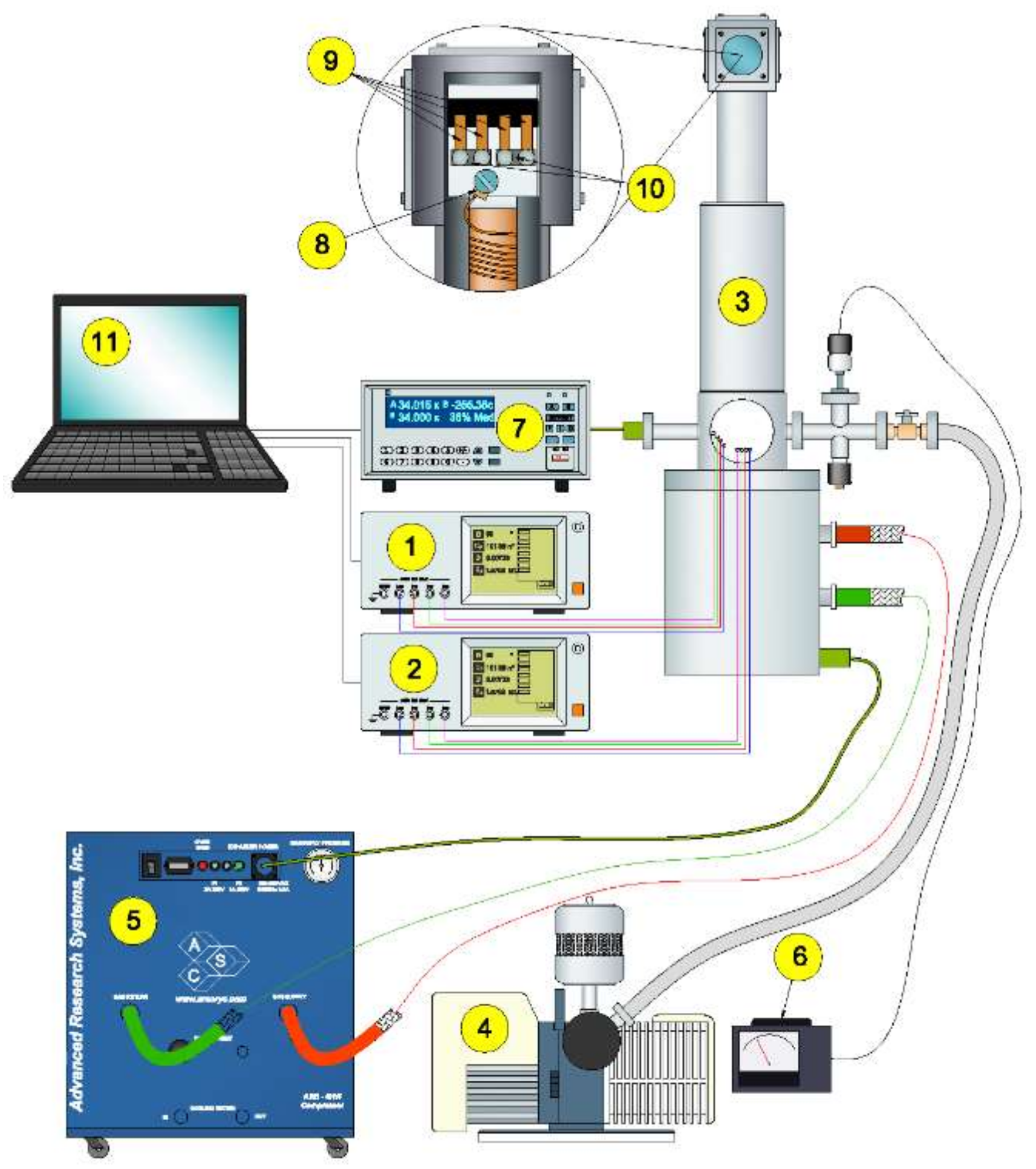
Alternating current measurements of MXene-PCL nanocomposites were carried out using a test stand developed and constructed at the Department of Electrical Devices and High Voltage Technology, Lublin University of Technology (Lublin, Poland). View of the test stand is shown in
Figure 1 [
23].
The stand includes the CS 204AE-FMX-1AL helium cryostat (Advanced Research Systems, Inc., Macungie, PA, USA) (3–7), which allows to measure temperatures in the range from 15 K to 450 K with an accuracy of 0.002 K. The entire measurement takes place under vacuum (~0.2 atm.), which is achieved using a vacuum pump (4). The tested nanocomposite sample (11) is placed in the cryostat head (3) and cooled in a closed circuit by means of a helium compressor (5). Temperature detection and control are carried out by a system consisting of a silicon sensor (8), a temperature controller (7), and a connected heater mounted in the cryostat head. Electrical parameters were measured every 1 K in the range 15 K–20 K, every 2 K in the range 20 K–40 K, every 3 K in the range 40 K–151 K, and every 7 K in the range 151 K–305 K. For the AC measurements, 3532 LCR HiTESTER (Hioki, Japan) impedance meters were used (1). The impedance meters have the ability to measure four of the following 14 electrical parameters: Z—impedance, Y—admittance, φ—phase shift angle, tg δ—loss factor, Q—Q factor, CS—static capacitance in series equivalent circuit, CP—static capacitance in parallel equivalent circuit, LS—inductance in series equivalent circuit, LP—inductance in parallel equivalent circuit, RS—effective resistance in series equivalent circuit, G—conductance, RP—effective resistance in parallel equivalent circuit, X—reactance, B—susceptance. The amplitude of the voltage applied to the test sample was U = 0.4 V. The impedance meter and the temperature controller are connected to a computer (11), where the measurement results are saved as xls files.
A program, written in the C++ environment, was developed to control the impedance meters and control and record electrical and temperature parameters. The program has the ability to select any four electrical parameters for simultaneous measurement and allows to enter specific values for measurement voltage and frequency range.
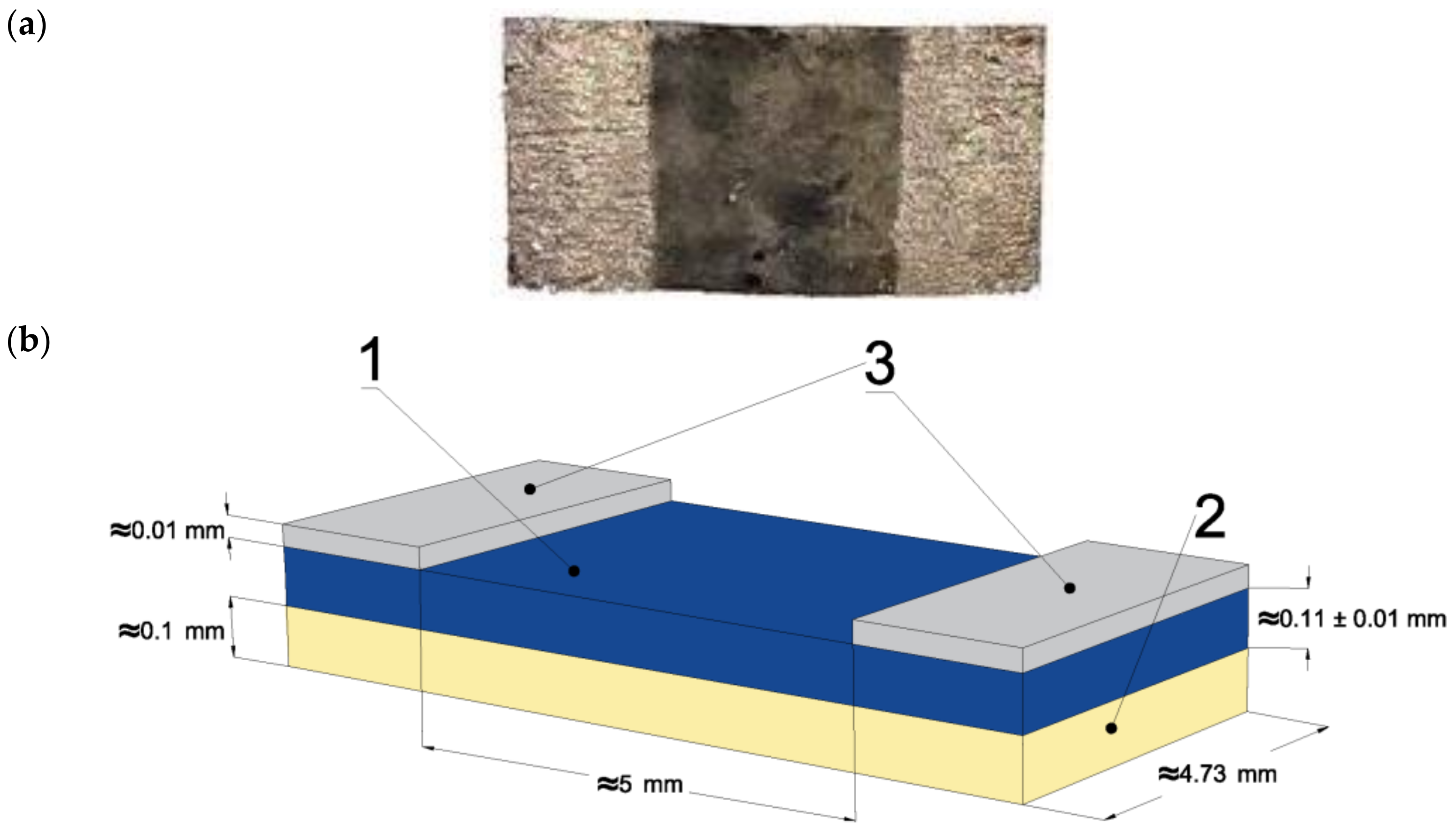
In this study, the AC properties of the MXene-PCL nanocomposite samples were investigated. At both ends of the tested nanocomposite, a thin layer (~10 µm) of silver paste was applied to eliminate the transition resistance at the point between the sample and the contacts (
Figure 2).
As shown in
Figure 2, the AC current applied at the ends of the nanocomposite layer flows between the two contacts. This means that both the real and imaginary components of the current, which consists of capacitive and inductive currents, flow between the same contacts. This means that these three currents flow in parallel in the nanocomposite layer. Therefore, a parallel equivalent impedance meter scheme was chosen to measure the alternating current parameters of the nanocomposite. Measurements were performed in the temperature range of 20 K to 305 K (70 temperatures) and frequencies from 50 Hz to 1 MHz with a step of 50 points per decade (about 240 frequency values). The following parameters were measured: phase shift angle
φ, inductance
Lp, and capacitance
Cp in the parallel equivalent scheme.
As is known [
24], there are two components of current in AC parallel circuits consisting of
RLC elements. The first one, the real (or resistive) component, is in a phase with applied sinusoidal voltage. Its value is determined by the formula:
where,
IR—real component of the current,
RP—parallel circuit resistance,
U—applied sinusoidal voltage.
The second component of the current, called the imaginary component, is determined by the value of susceptance
B:
where,
B—susceptance,
ω = 2π—circular frequency,
CP—parallel circuit capacitance,
LP—parallel circuit inductance.
Using the value of susceptance
B, the value of the imaginary component of current
II is calculated:
where,
II—imaginary component of the current.
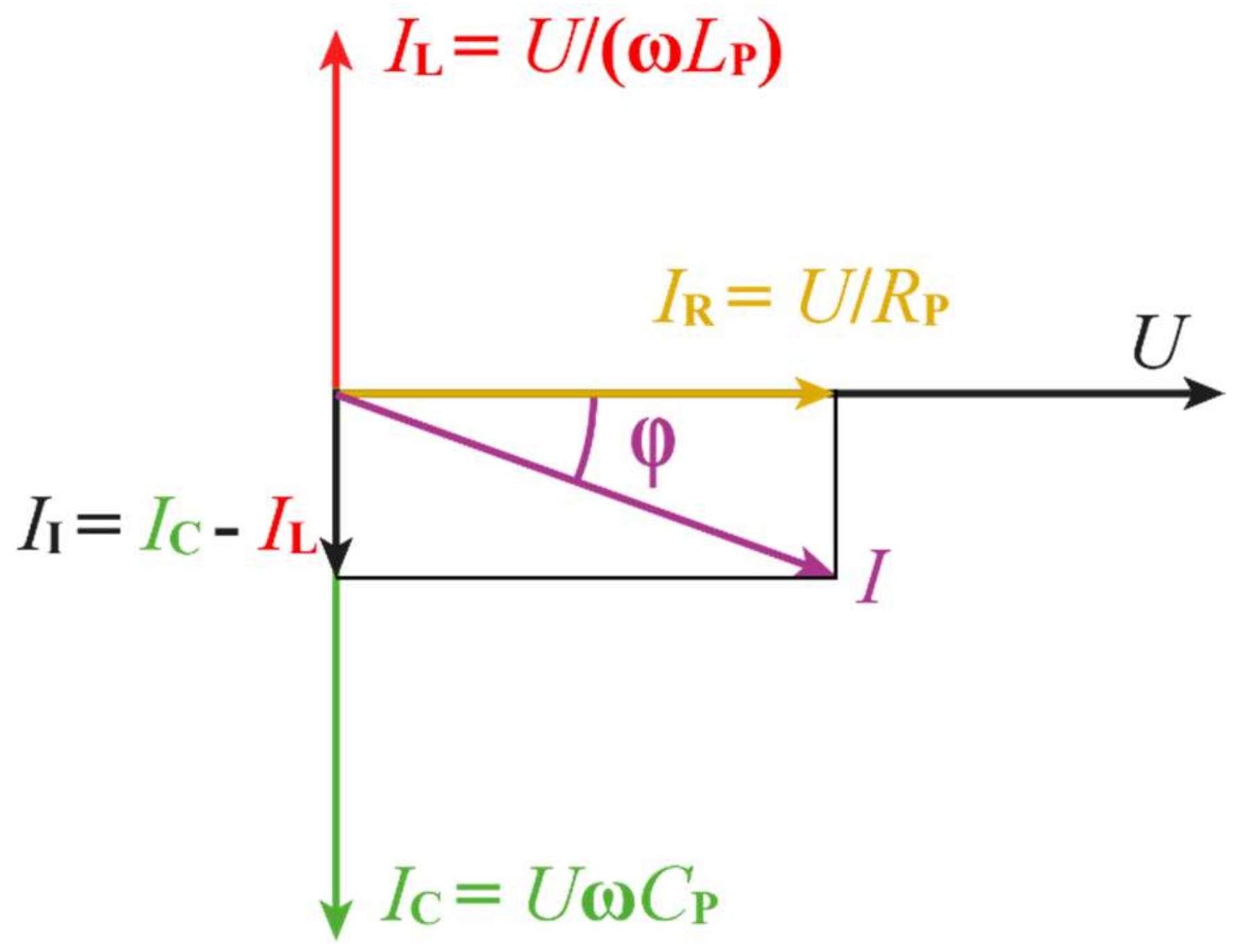
The vector of the imaginary component is perpendicular to the real current vector. The value of the angle modulus between these vectors is 90°. The sign of this angle depends on which component of susceptance (capacitive or inductive) from Formula (2) is higher. When the capacitive component is higher, the sign of the angle is negative and when the inductive component is higher, the sign of the angle is positive. One of the basic alternating current parameters of the parallel
RLC circuit is the phase shift angle between the vector of the real current component and the resultant current vector (
Figure 3). The phase shift angle value is calculated from the formula:
where,
φ—phase shift angle.
Figure 3 shows a phasor diagram of the AC sinusoidal current’s real and imaginary components for a parallel
RLC circuit in case the capacitive component is larger than the inductive component.
In parallel
RLC circuits at the resonant circular frequency
ωr = 2π
fr, a parallel resonance [
25] occurs. From Formula (2) for susceptance, it follows that at the value of resonant circular frequency
ωr, the modules of capacitive and inductive components of susceptance are equal and their difference is equal to zero.
The value of the resonant circular frequency for a parallel circuit is determined by the formula:
where,
ωr—resonant circular frequency.
Let us now examine how to measure the experimental frequency dependence of the capacitance and inductance of the MXene-PCL nanocomposites using the 3532 LCR HiTESTER impedance meter. The method of measurement and formulas for calculating the parameters are given in the user manual [
26]. According to the user manual, after applying sinusoidal voltage
U to the tested circuit, in the first stage, the meter calculates the phase shift angle
φ between the vectors of voltage
U and current
I (see
Figure 3) and the circular frequency
ω = 2π
f. In the second stage, based on three values:
U,
I, and
φ, the other parameters of the circuit under test are calculated using the formulas given in the manual. For the purposes of this work, the following formulas are needed:
where,
Y—admittance.
where,
B—susceptance.
where,
CPM—the capacitance value measured by the impedance meter.
We will now determine the relationship between the actual value of the capacitance of the parallel circuit and the value measured by the impedance meter. By substituting into Equation (8) the value of susceptance
B from Equation (2) we obtain:
where,
CP—actual value of capacitance in the tested parallel circuit,
LP—actual value of inductance in the tested parallel circuit.
Formula (9) shows that the measured capacitance is smaller than the actual one. The result of the capacitance measurement coincides with its actual value only if there is no inductance in the circuit under test. The value of the measured capacitance in the case of φ > 0° should not be taken into account.
By substituting the value of the resonant circular frequency (5) into the formula for the measured value of capacitance (9), we obtain:
Formula (10) shows that at the resonant circular frequency, the measured capacitance of the circuit should be zero. When the circular frequency ω approaches the resonant value from the side of lower values, the value of the measured capacitance becomes smaller and smaller, and at the resonant circular frequency ωr, its value, theoretically, is zero. A further increase in the circular frequency will increase the measured capacitance. This means that there will be a clear minimum in the frequency dependence of the measured capacitance. It is one of the criteria that allows to observe the parallel resonance and determine the value of the resonant circular frequency ωr.
According to the user manual, the meter performs the calculation of inductance based on the formula:
By substituting into Formula (11) the value of susceptance given by Formula (2), we obtain:
Formula (12) shows that the inductance of a parallel circuit is measured correctly only in the absence of capacitance.
By substituting the value of the resonant circular frequency (5) into Formula (12) for the measured inductance, we obtain:
As the frequency approaches its resonance value, the measured inductance begins to increase, reaching its maximum value at the resonance frequency. A further frequency increase causes the measured value to decrease.
4. Results and Discussion
Figure 4a–c represented results of XRD and SEM analysis of prepared MXene, respectively. The XRD pattern in
Figure 4a indicates that the obtained material is pure Ti
3C
2 MXene. SEM demonstrates that MXene has a typical shape, with a size from 25 to 500 nm.
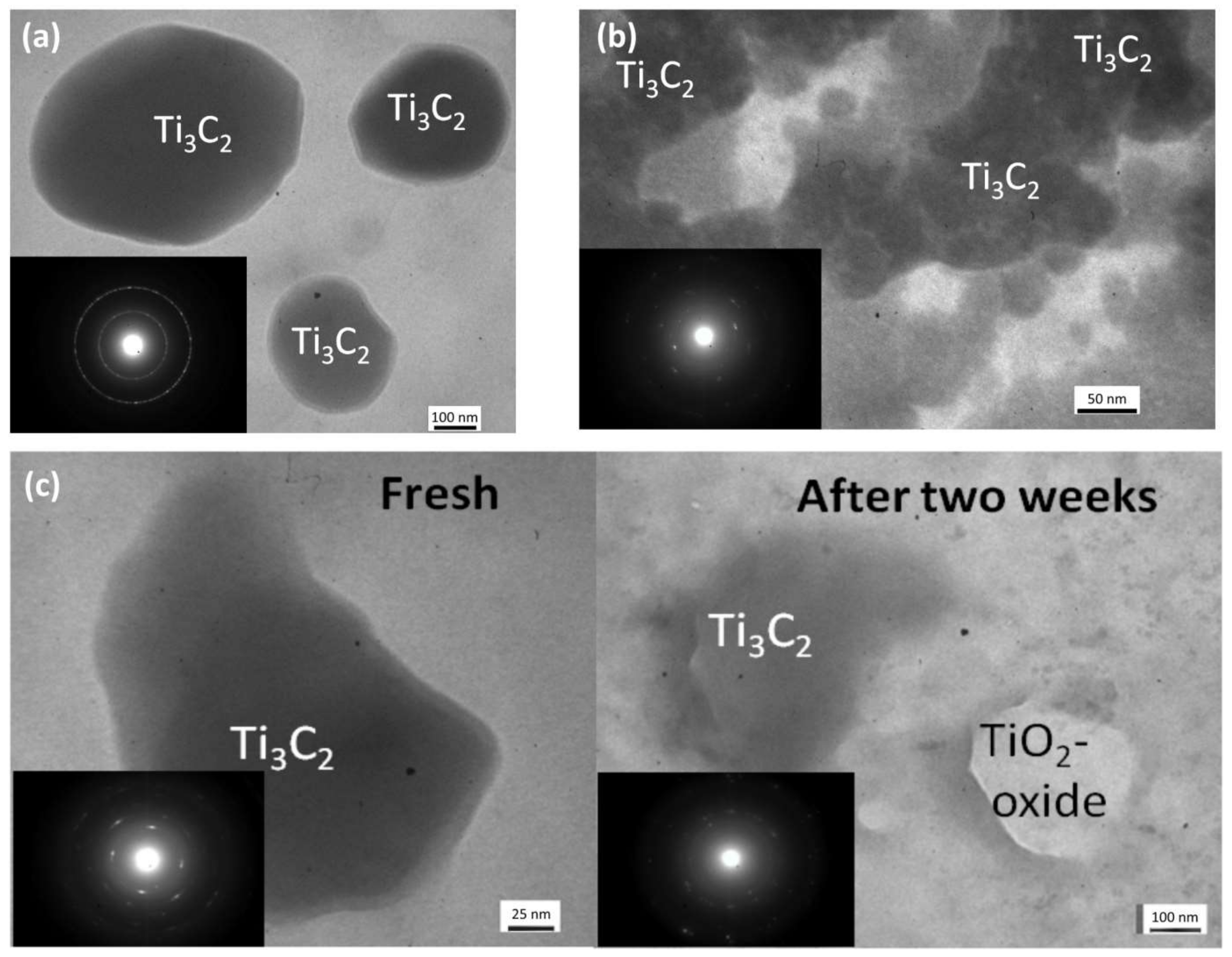
Figure 5a,b represents the dark-field images of pure Ti
3C
2T
x MXene samples. It seems that the samples exhibit good exfoliation. In some regions, MXenes are almost transparent to the electron beam because the thickness is close to several atomic distances [
27]. Further analysis of SAED from the flakes revealed the Ti
3C
2 hexagonal lattice of high crystallinity [
28]. Titanium distribution in the crystal lattice ensures good electrical conductivity. Depending on the concentration and thickness (periodicity of layers), the MXenes crystal structure varies from single crystal to polycrystalline-like. Lattice parameters were increased in the tabular Ti
3C
2 structure (hexagonal P63/mmc symmetry)
a = 3.183 Å (
atab = 3.071 Å),
c = 15.68 Å (
ctab = 15.131 Å). Test samples were then exposed to air for two weeks to analyse the oxidation behaviour. As a result of the analysis, the crystallinity of the samples was dropped (
Figure 5c). Some flakes exhibit the transition to titanium dioxide, but only local decomposition to oxygen compounds was observed. Moreover, under the thermal effect of the electron beam, the structure of the MXene layers was changed instantly. White areas changed to black, which meant that oxidation of the specimens was only partial and potentially reversible after the thermal annealing.
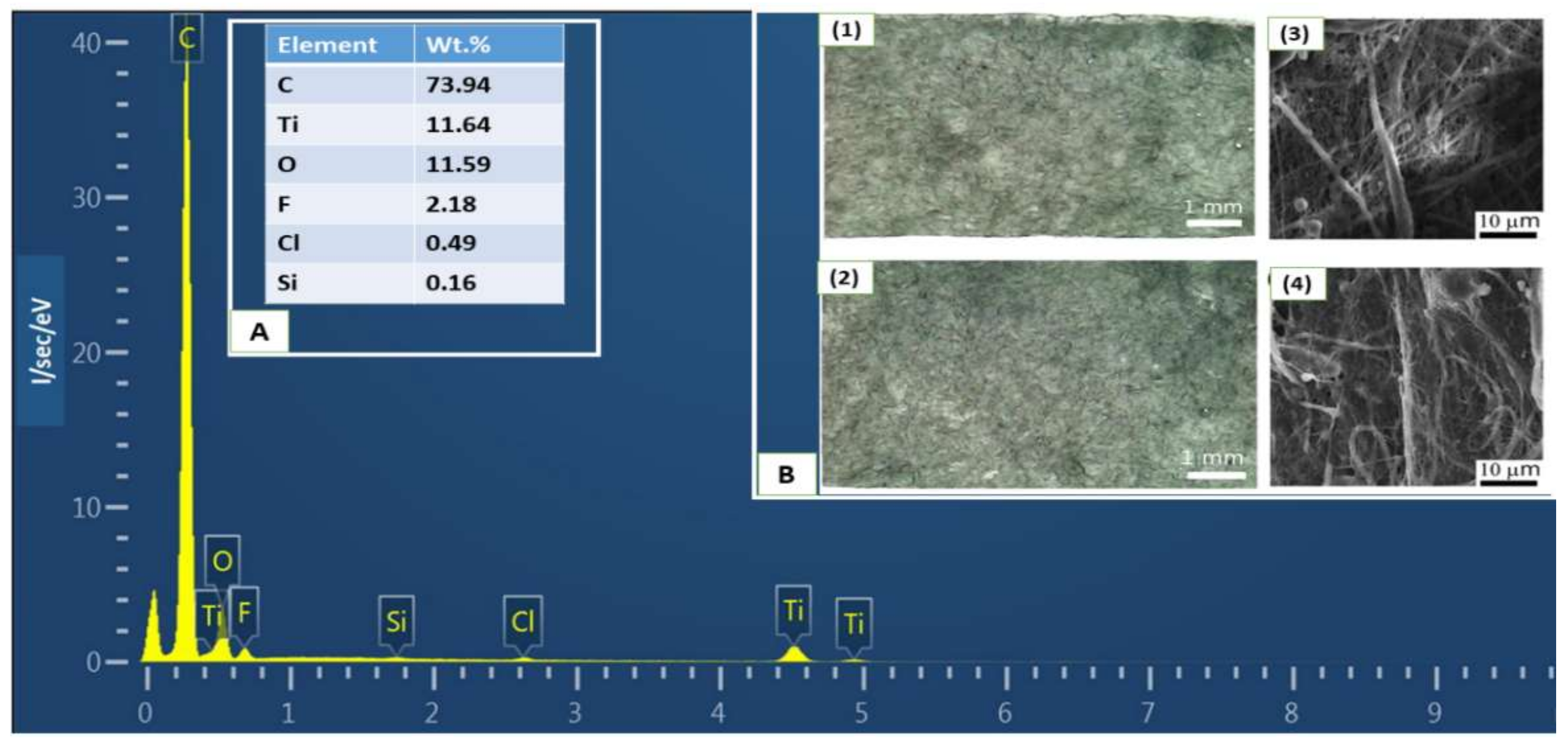
After MXene was coated on the PCL photomicrograph, an EDS scan was taken (
Figure 6). It seems that the distribution of fibers is random, with an average diameter of 1.41 ± 0.33 μm. The structure is similar to pristine PCL with unified MXene flakes along the fibers. MXene nanosheets occupy most of the space, which is very good for electron transport. The chemical composition derived from EDS is consistent with articles by other authors [
8,
29]. The most intensive signal (~74%) is from the C-Kα line since both PCL and Ti
3C
2 contains it. O, F, and Cl signals suggest that MXene exhibits a binding with the functional groups. No Al concentration was observed. Thus, it was completely removed during the precursor exfoliation.
Samples of the MXene-PCL nanocomposites were chosen for the analysis in order to obtain clear and original results.
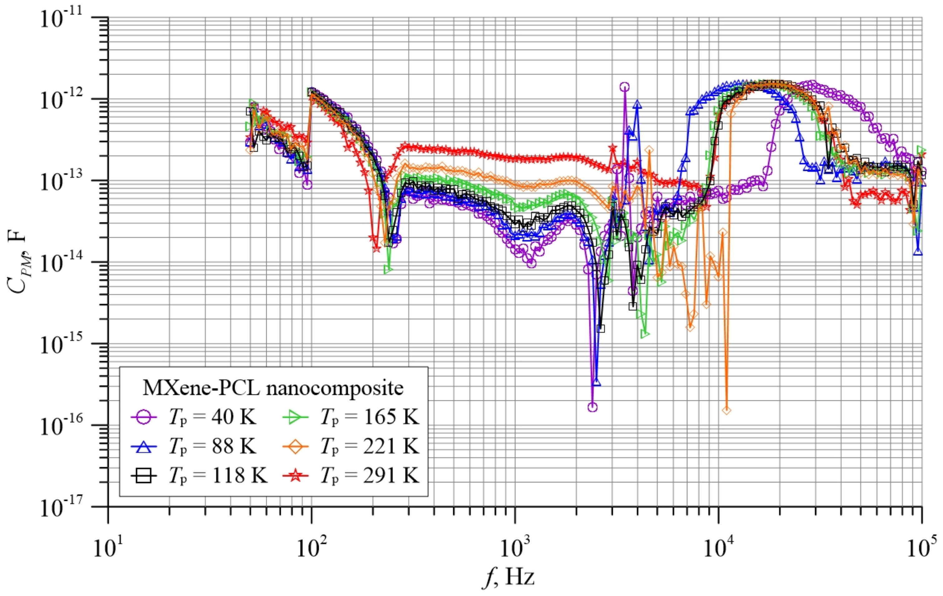
Figure 7 shows the frequency dependence of the capacitances measured in the parallel equivalent scheme. The figure shows six waveforms in the temperature range of 20 K–305 K, selected from 70 waveforms obtained during the measurements. The measurements, in order to precisely determine the positions of the minima, were performed at 50 points per decade.
The capacitance values measured in the parallel equivalent circuit diagram slowly decrease with increasing frequency. The values are in the range of 1.7 × 10
−12 pF to about 4 × 10
−13 pF. Such low capacitance values occur due to the shape of the sample, together with the contacts applied to it (
Figure 2). As can be seen from the figure, the area of the measured sample is equal to the cross-sectional area of the nanocomposite layer. The thickness of the dielectric is equal to the distance between the contacts. This results in the capacitance of the sample being very low. From the frequency dependence of the measured capacitances, shown in
Figure 7, it can be seen that the MXene-PCL nanocomposite exhibits a series of minima against a background of a slow decrease of capacitance with frequency increase. Some of them are very clear. These are minima at frequencies of around 100 Hz, around 200 Hz, around 1100 Hz and around 2200 Hz. In the frequency range above 2200 Hz, further sharp minima are observed. However, determining the frequency values at which they are observed is relatively difficult due to their very close proximity. The only thing is that these minima practically disappear at room temperature. A broad clear maximum is observed in the frequency range from about 10
4 Hz to about 10
5 Hz. The position of the maximum, depending on the temperature, occurs at frequencies from about 1.3 × 10
4 Hz to about 3 × 10
4 Hz. In the frequency range above 10
5 Hz, oscillations of large amplitudes occur that completely interfere with the capacitance measurements. Oscillations of this type were not observed by us for other types of nanocomposites [
30,
31,
32]. The oscillations are probably related to the unique structure of the MXene-PCL nanocomposites. Explanation of their causes requires additional research, far beyond the scope of this article. Accordingly, this paper focuses on the analysis of the behaviour of the minima observed in the frequency range up to 10
5 Hz. Therefore, in
Figure 7,
Figure 8 and
Figure 9, the frequency range is limited to 10
5 Hz.
As can be seen from Equation (10), the capacitance values at the minima should be zero. This is consistent for a parallel
RLC circuit, whose resistance is zero. In the case of non-zero resistance, the depth of the minimum is smaller, which is also observed in
Figure 7. A second factor, reducing the depth of the minimum, is that measurements were made for 50 points per decade. This means that it was difficult to precisely hit the value of the resonant frequency. As a result of missing such hits, the measured capacitance for a given minimum does not reach zero. The minimum at 2200 Hz is closest to the resonance frequency, and its depth is more than two orders. In conventional parallel
RLC circuits consisting of discrete elements, there is only one minimum. This is due to the fact that the values of the discrete elements are constant values. However, in nanocomposites, capacitance and inductance values are functions of the frequency, morphology, and structure of the nanomaterial [
33,
34]. This allows a greater number of frequencies to occur in the nanocomposite at which parallel resonance is observed.
We will now analyse the effect of temperature on the minima occurring at frequencies of around 100 Hz, around 200 Hz, around 1100 Hz, and around 2200 Hz. It can be seen from
Figure 7 that the depth of the minimum at about 100 Hz practically does not depend on the temperature. A similar situation is also characteristic for the minimum at around 200 Hz. An increase in the temperature value causes a slight shift of the minimum position into the area of lower frequencies. The temperature increase practically does not change position of minimum around 1100 Hz, but it clearly reduces its depth. At 291 K, this minimum almost disappears. The next minimum at around 2200 Hz shifts slightly into the higher frequency region as the temperature increases. The depth of this minimum reaches more than two orders and decreases rapidly with increasing temperature. The depth of minima, located in the frequency region (10
4–10
5) Hz, also decreases rapidly with increasing temperature and disappears at room temperature. This means that there are at least two types of tunneling between nanoparticles in the nanocomposite, which become apparent in the form of
CPM minima. This is evidenced by the different way in which the depth of the minima changes under the influence of temperature. For the minima of the first group (at 100 Hz and 200 Hz), their depth practically does not depend on temperature. For the second group (1100 Hz and 2200 Hz and minima in the frequency region (10
4–10
5) Hz)), the depth of the minima decreases very rapidly with increasing temperature. At room temperature, the minima of the second group practically disappear. The two different types of tunneling can be related to the different morphologies and structures of the nanoparticles between which tunneling takes place.
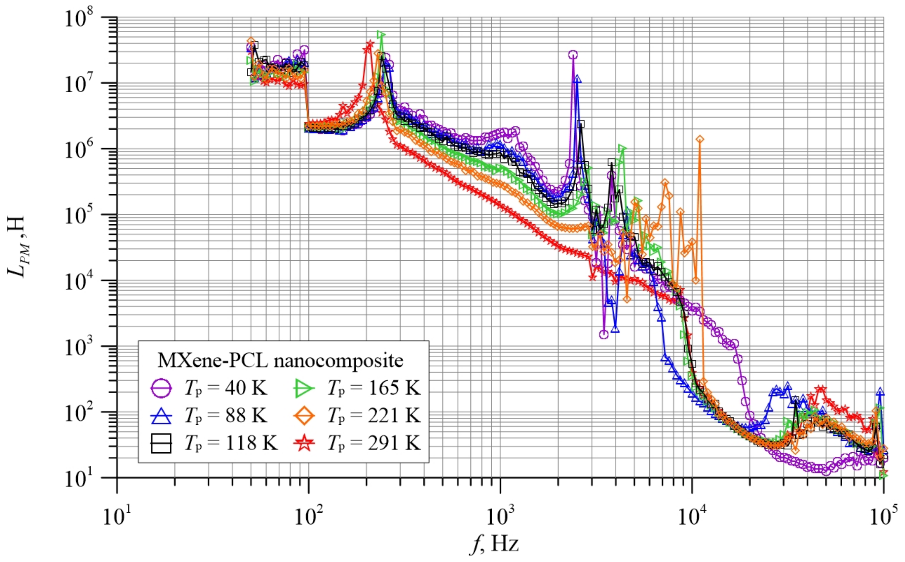
The frequency dependence of the MXene-PCL nanocomposite inductance measured in the parallel equivalent scheme is shown in
Figure 8. Only 6 waveforms, selected from 70, obtained during the tests for temperatures ranging from 20 K to 305 K, are shown in the figure. As can be seen from
Figure 8, there are a number of maxima on the frequency dependence of
LPM(
f). Their positions exactly match the positions of the minima on the frequency dependence of the measured capacitances, shown in
Figure 7. This means that the frequencies at which inductance maxima occur are the frequencies for which parallel resonance occur. The value of inductance measured at maxima for a circuit not containing resistance should be infinity—Formula (13). The presence of a resistance causes the value at maximum of the measured inductance to be lower. A second factor lowering the value at maximum is that the measurements were made with a step of 50 points per decade. As a result of the simultaneous interaction of these two factors, the inductance at the maximum does not reach infinity. The maximum at 2200 Hz is closest to the resonance frequency. Its amplitude is about two orders. Wide clear minima are observed on the
LPM(
f) relation at frequencies from about 1.3 × 10
4 Hz to about 3 × 10
4 Hz—depending on the temperature. The positions of the minima of the measured inductances (
Figure 8) exactly coincide with the positions of the maxima on the frequency dependence of the measured capacitances (
Figure 7). In the frequency range above 2200 Hz to about 10,000 Hz, further sharp maxima are observed.
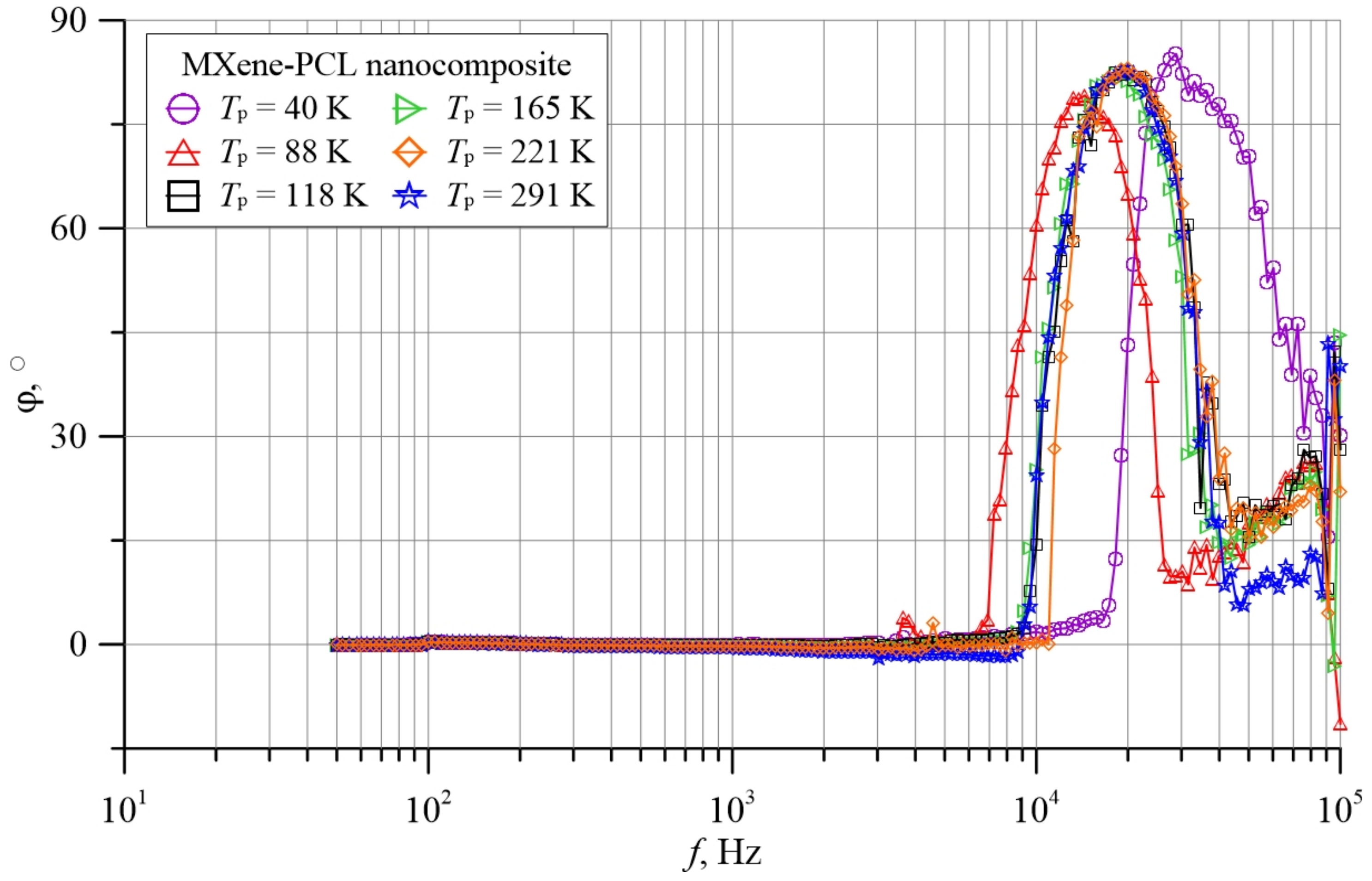
Figure 9 shows 6 selected from 70 frequency dependencies of the MXene-PCL phase shift angle
φ, obtained for temperatures ranging from 20 K to 305 K. The measurements, in order to precisely determine the frequencies in which the maximum occurs, were made at 50 points per decade.
The figure shows that up to a frequency of about 10
3 Hz, the values of the phase shift angle are close to 0°. With further frequency increase practically up to about 10
4 Hz, the values of the phase shift angle are weakly negative. It follows that in this frequency region, the capacitive component of the conductivity is slightly larger than the inductive component. Beyond a frequency of 10
4 Hz, the values of the phase shift angle become positive. As can be seen from
Figure 9, in the frequency region from about 10
4 Hz to about 10
5 Hz, an increase in positive phase angle values is observed and a maximum is reached, the value of which ranges from about 80° to about 85°, depending on the temperature. A further increase in frequency causes a decrease in the value of the phase shift angle—the values of which remain positive. This means that in this frequency range, the inductive component of the conductivity of the MXene-PCL nanocomposite is many times greater than the capacitive component. This phase shift angle behavior occurs in a range of nanocomposites containing conductive phase nanoparticles in dielectric matrices [
35,
36,
37,
38,
39,
40]—both capacitive and inductive components were observed in them.
It should be noted that in conventional
RLC circuits, inductance occurs, as a rule, in the form of a coil wound from a thin conductor. In the nanocomposite layers studied, there were no windings (
Figure 2). The occurrence of a phase shift in them, characteristic of coils, is related to the conduction mechanism based on the phenomenon of electron tunneling between neighbouring nanoparticles [
41]. This paper [
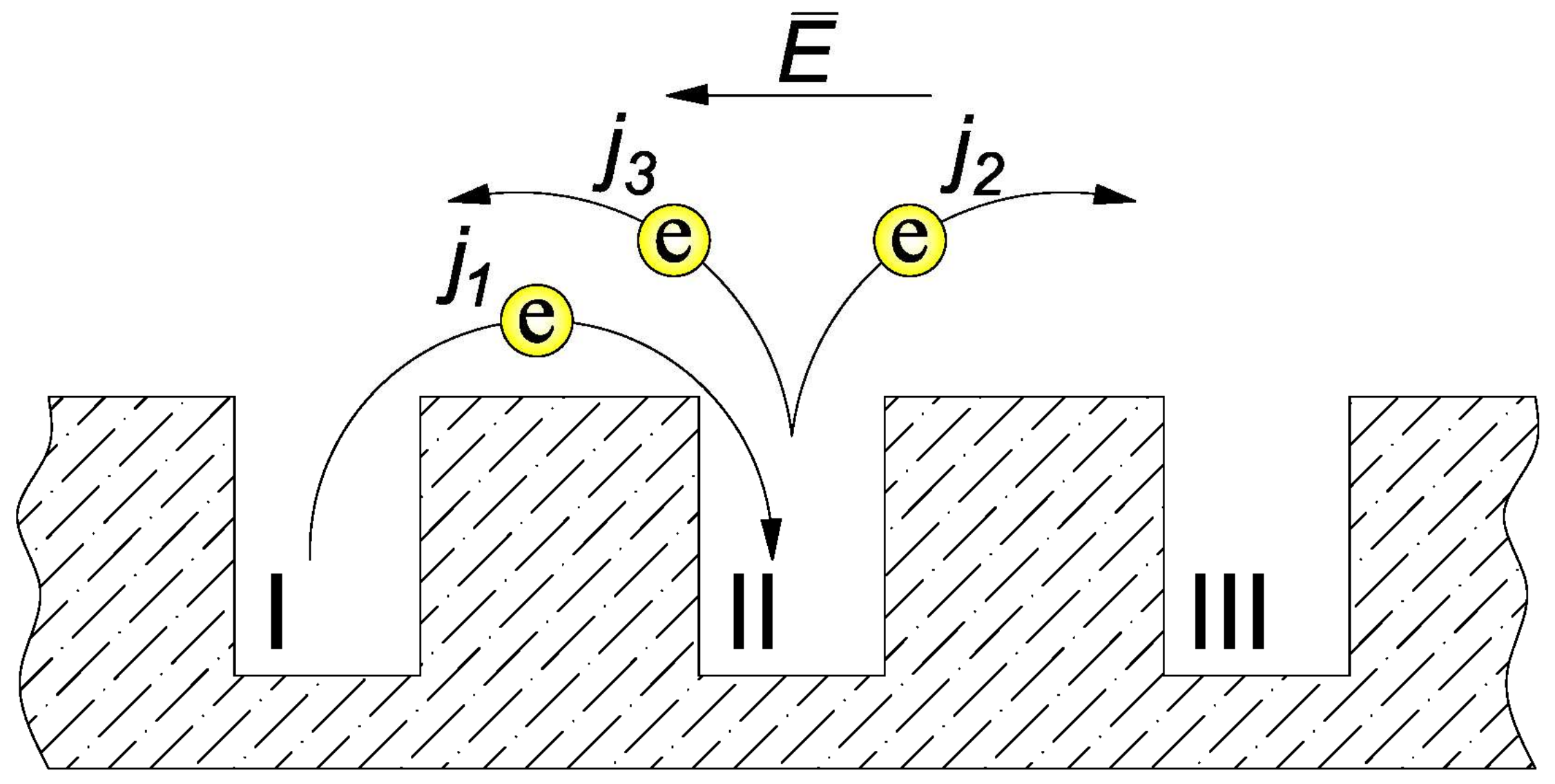
41] presents an impedance model and its experimental verification for nanocomposites in which conductivity takes place by electron tunneling between nanoparticles. The model assumes that there are nanometer-sized potential wells in the material where electrons are located (
Figure 10). Distances between the wells are also nanometric. This allows the electrons to tunnel between neighbouring wells of the potential, defined by the following formula [
42,
43]:
where,
r—distance over which the electron is tunneling,
α—value close to the inverse of the radius of location of the tunneling electron (so called Bohr radius),
β—numerical coefficient close to 2 [
44], Δ
W—activation energy of electron tunneling,
k—Boltzman’s constant,
T—temperature,
P0—numerical factor.
The electric field forcing the current flow is weak and does not change the probability of electrons tunneling from one neutral potential well to another. The field only leads to an asymmetry of the jumps, related to the Debye factor [
44]:
where,
e—charge of the electron,
r—distance the electron tunneling,
E—electric field strength.
The value of a weak electric field can be defined as:
where,
E0—amplitude of the electric field strength.
Under the influence of this field (on the tunneling path between adjacent potential wells) flow, a current of density (
Figure 10):
where,
σ—conductivity.
The electron, after tunneling into the second well, remains there for relaxation time
τ. The value of the relaxation time is a function of the temperature and the distance over which the electron tunnels [
45]. After the relaxation time, two variants of tunneling are possible. In the first one, the electron with probability
p tunnels to the next (third) well in the direction determined by the forcing electric field (
Figure 10). This results in a second component of the current density:
In the second variant, the electron after relaxation time
τ tunnels from the second well to the first one (
Figure 10) with probability (1−
p). This results in the appearance of the third component of current density:
Equations (17)–(19) can be used for the temperature region T < 500 K, when values p(T)τ << 1 (see Formula (14)).
This means that the resultant current density, due to electron tunneling, has both a real and an imaginary component.
We will now extract the real and imaginary components of the tunneling current density from Equations (17)–(19). The current density j1 is in the same phase as the forcing electric field and therefore contains only the real component.
The
j2 and
j3 components are in an equal phase. Hence:
From Formulas (17) and (20), it follows that the real component of the tunneling current density is:
and the imaginary component of the current density due to tunneling is:
The phase shift angle between the real (21) and imaginary (22) components of the current density due to tunneling is:
By substituting the value of
θ into Equations (21) and (22), we obtain:
A material of the same composition as the nanocomposite, in the absence of tunneling in it, has a dielectric permittivity
εr > 1. This means that, according to Maxwell’s second equation, there will be a component of capacitive current flowing through the material that is not related to electron tunneling. The density of this current component is described by the following formula [
46]:
where,
εr—relative dielectric permittivity,
ε0—dielectric permittivity of vacuum.
The total density of the imaginary component of the current, taking into account Formulas (22) and (26), is:
The phase shift angle between the real and imaginary components of the current density is:
From Equation (28), it follows that the value of the phase shift angle is a function of conductivity σ, dielectric permittivity
εr, relaxation time
τ and frequency
ω. From Equation (28), it follows that in the low frequency region, where:
Formula (28) transforms to the form:
Equation (30) shows that for low frequency values (ωτ << 2σp), the phase shift angle φ is negative and close to zero.
In the paper [
41], computer simulations were performed based on Equation (28). They show that with further increase of frequency depending on the conductivity value
σ, the following cases can occur:
- (a)
For low conductivity values in the low frequency range, the phase shift angle
φ is approximately equal to 0° and a decrease of the phase shift angle value to about −90° with stabilization at this level is observed. This situation occurs, according to Equation (28), in the high frequency region when:
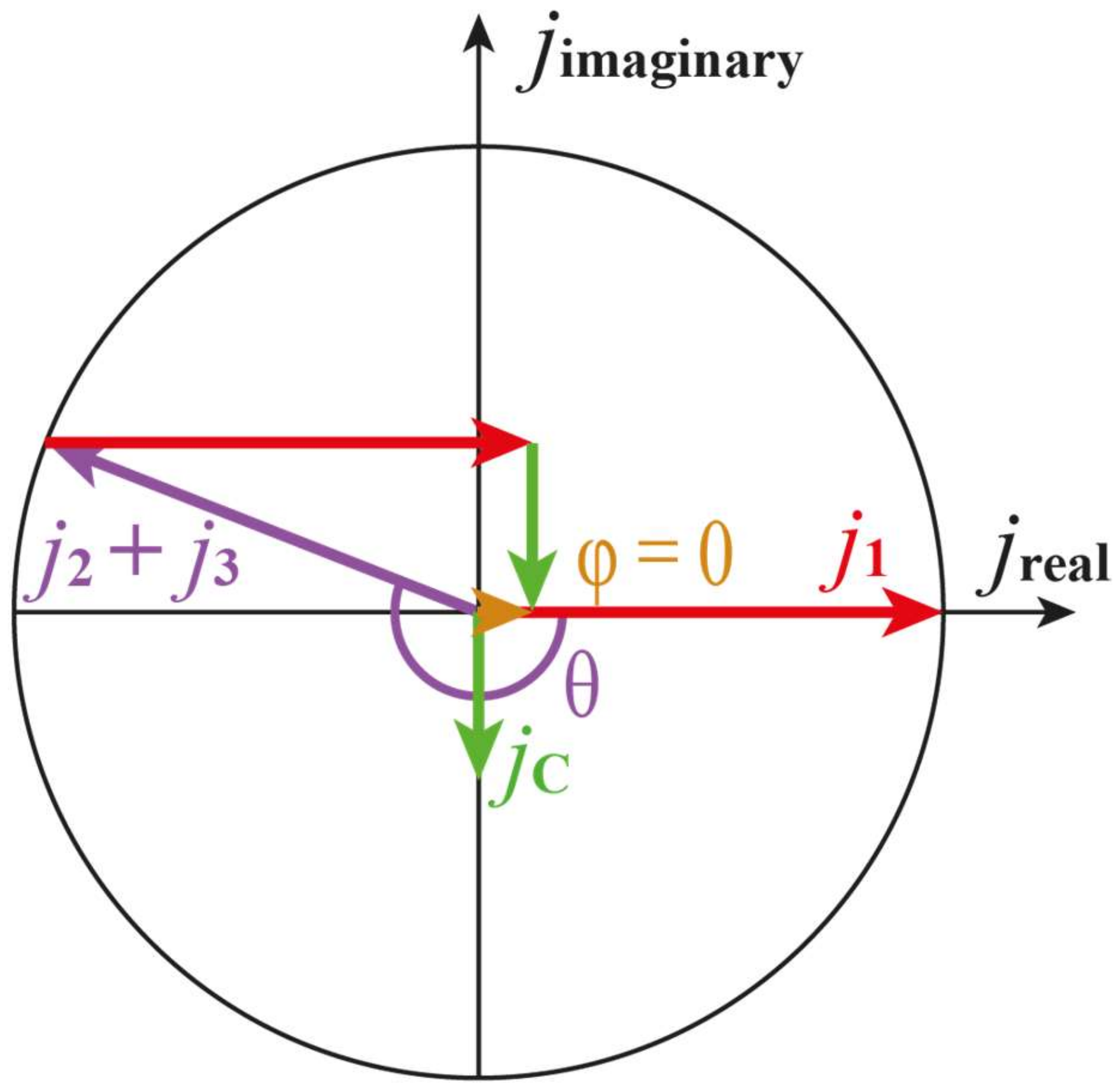
An indication diagram for this case is shown in
Figure 11.
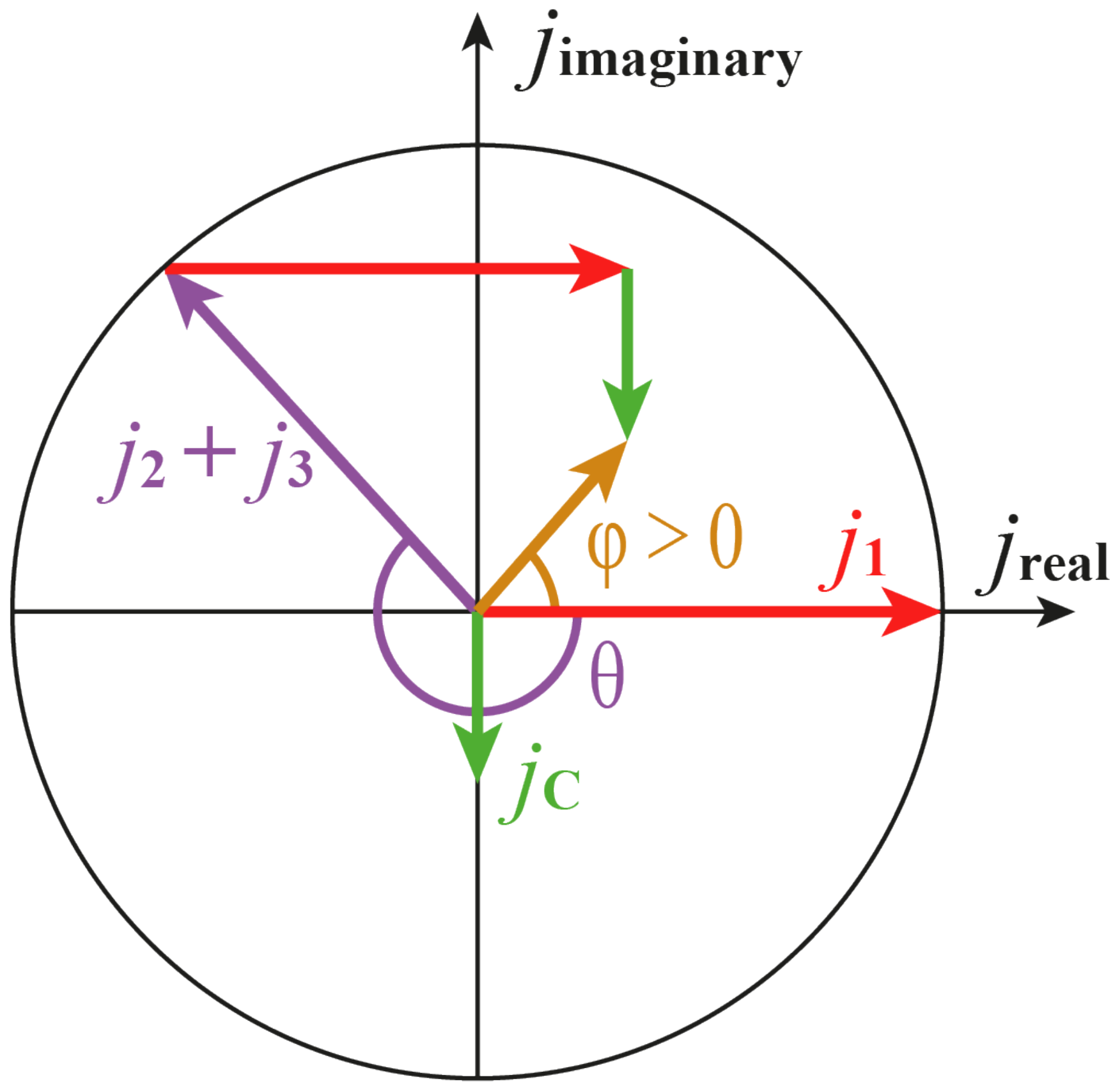
- (b)
For average conductivity values, the phase shift angle
φ waveforms show values close to zero in the low frequency region. An increase of frequency causes an increase of negative values until a minimum is reached. After crossing zero, positive values of the phase shift angle occur, passing through the maximum and then decreasing the phase shift angle. The zero crossing at frequency
ωr corresponds to the phenomenon of parallel resonance. From Equations (22) and (28), it follows that
φ = 0° occurs when:
An indication diagram for the case of parallel resonance is shown in
Figure 12.
- (c)
For high values of conductivity, when
σ >> εrε0ω and medium values of frequency, positive values of the phase shift angle occur. When the maximum is reached, the value of which
φmax ≈ 90°, a decrease in the phase shift angle value takes place. An indication graph for this case is shown in
Figure 13.
Figure 12 shows that the angle θ between the
j1 and
j2 +
j3 components at the resonance frequency is slightly more than −
π. From the value of the frequency at the inductance maximum of about 8×10
4 Hz and using Formula (23), it is possible to determine the values of the relaxation times τ for the individual sharp maxima observed in
Figure 8. For maximum at frequency
f1 ≈ 100 Hz,
τ1 ≈ 5×10
−3 s; for
f2 ≈ 200 Hz,
τ2 ≈ 2.5 × 10
−3 s; for
f3 ≈ 1100 Hz
τ3 ≈ 4.5 × 10
−4 s, and for
f4 ≈ 2200 Hz,
τ4 ≈ 2.3×10
−4 s.
As can be seen from
Figure 9, in the frequency range
f < 10
4 Hz, there are close to zero values of the phase shift angle. This means that resistive conduction is dominant in this range. The series resonance observed in this range (
Figure 7 and
Figure 8) prove that apart from resistive conduction, capacitance and inductance are simultaneously present. If the nanocomposite layer had a resistive conductivity and only one of the imaginary components, inductive or capacitive, the resonance of the currents would not occur.
This means that in the MXene-PCL nanocomposite, at least two types of nanoparticles are involved in tunneling in this frequency range. This is due to differences in the behavior of the amplitudes and frequencies of the individual minima induced by the temperature change. The two types of tunneling occurring in this frequency range belong to the case of average conductivity values, described in (b), Formula (28) and (32). An indication diagram is shown in
Figure 12. In the region from about 10
4 Hz to about 10
5 Hz, there is a broad maximum of the phase shift angle, values in which are 80° ≤
φ ≤ ~85° (
Figure 9). The position of the maximum is at frequencies from about 1.3 × 10
4 Hz to about 3 × 10
4 Hz, depending on the temperature. This situation is described in (c)—Equation (28). The appearance of a wide maximum at frequencies from about 10
4 Hz to about 10
5 Hz means that this is associated with a case of dominant conduction of the inductive type—as shown in case (c). This shows that a third type of tunneling occurs in the MXene-PCL nanocomposite. From the value of the frequency at the maximum of the phase shift angle, the expected value of the relaxation time was determined. At 40 K, it is
τM ≈ 8 × 10
−5 s. The occurrence of at least three types of tunneling in the MXene-PCL nanocomposite, with different relaxation times, is probably related to differences in the morphology and structure of the nanoparticles between which tunneling takes place and the distances over which electrons tunnel.
From calculations based on the amplitude and frequency of the position of the wide maximum (
Figure 8), the actual value of the inductance of the MXene-PCL nanocomposite layer was determined to be
LP (4 × 10
4 Hz) ≈ 1 H. It is important to consider what causes the nanocomposite layer to have such a high inductance. For this, we use the formula for the inductance value of a conventional coil without a ferromagnetic core given in [
25]:
where,
μ0—magnetic permittivity of vacuum,
n—number of coils per unit length,
v—volume of coil.
By transforming Equation (33), we obtain the “distance between neighbouring coil windings” from the nanocomposite:
Using this formula, obviously with a high degree of approximation, it is possible to determine the geometric dimensions of a single “coil” formed by the nanocomposite. By substituting into Equation (34) the values of
LP (4 × 10
4 Hz) ≈ 1 H,
μ0 and the values of geometrical dimensions of the nanocomposite sample from
Figure 2, we obtain the “distance between neighbouring coil windings” of the nanocomposite, which is about ∆
l ≈ 5.7 nm. As noted above, conduction in the nanocomposite occurs by electron tunneling between neighbouring nanoparticles. After each jump, the electron remains for a relaxation time
τ in the nanoparticle on which it has tunneled and thus causes a phase shift between the real and imaginary components of the current density due to tunneling (see Equations (18)–(23)). There is some analogy here with an induction coil, where each coil affects the phase shift of the current. This may mean that the “distance between neighbouring coil windings” from the nanocomposite obtained from Equation (34) is, to a large approximation, the expected value of the distance over which the electron tunnels.


 ,
, 


