
Easily Prepared Transparent Electrodes for Low-Cost Semitransparent Inverted Polymer Solar Cells

Abstract
:
1. Introduction
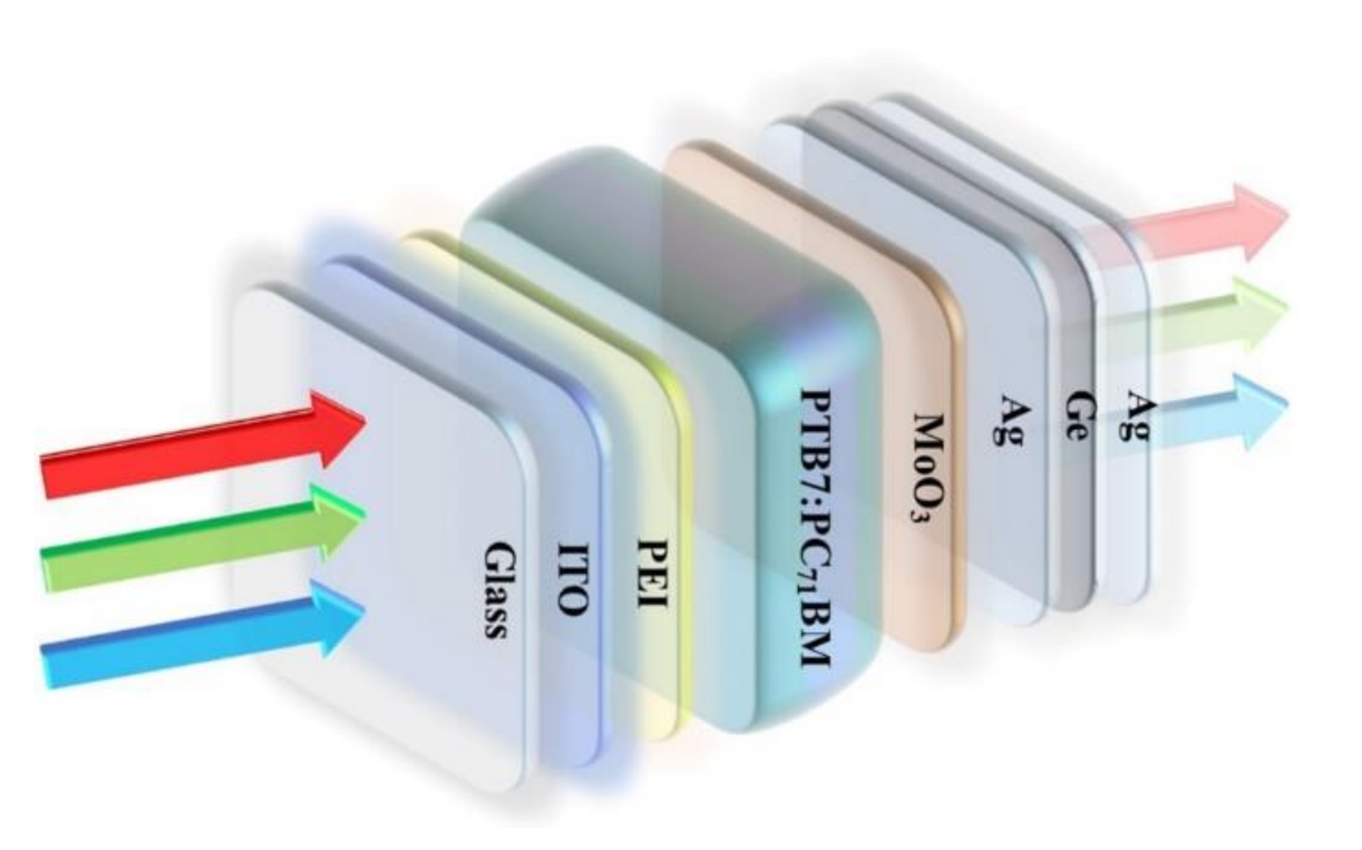
2. Experimental
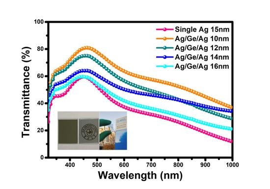
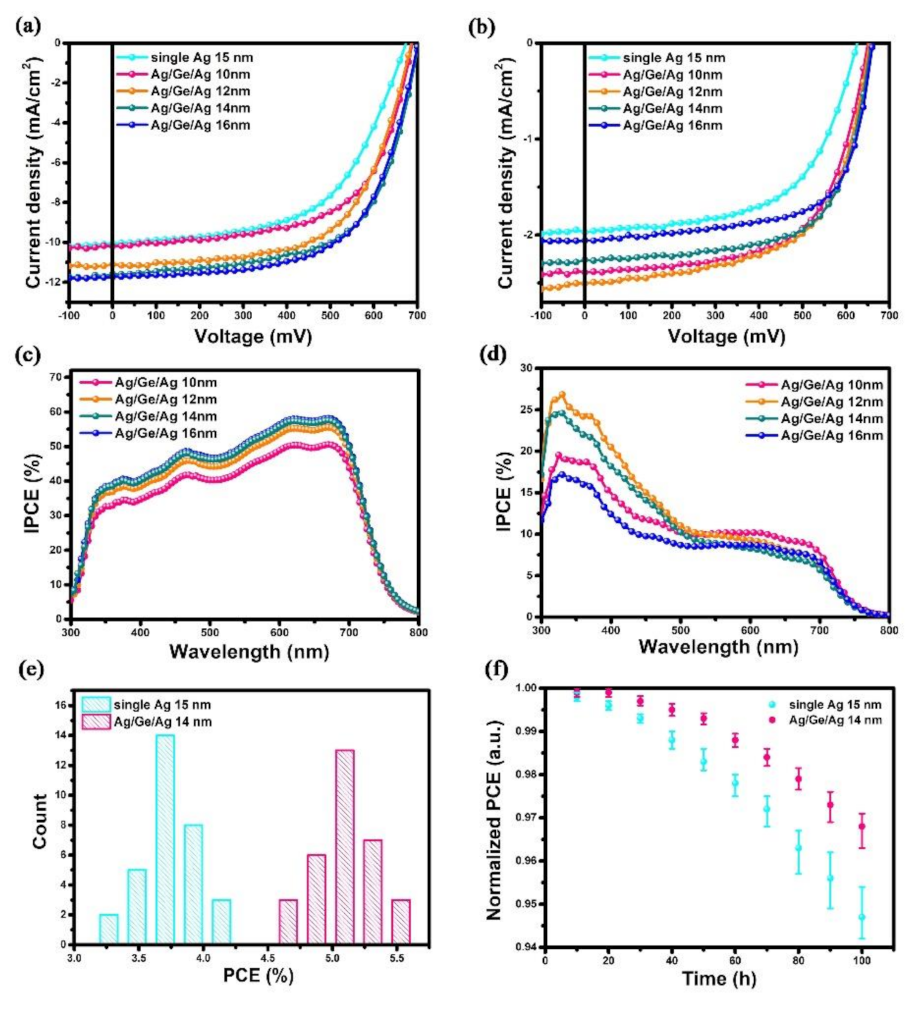
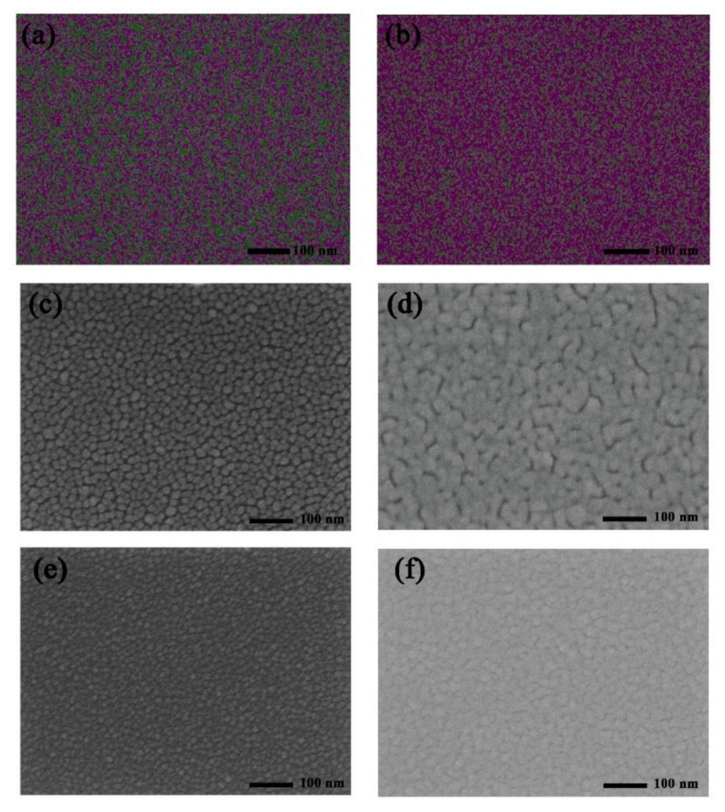
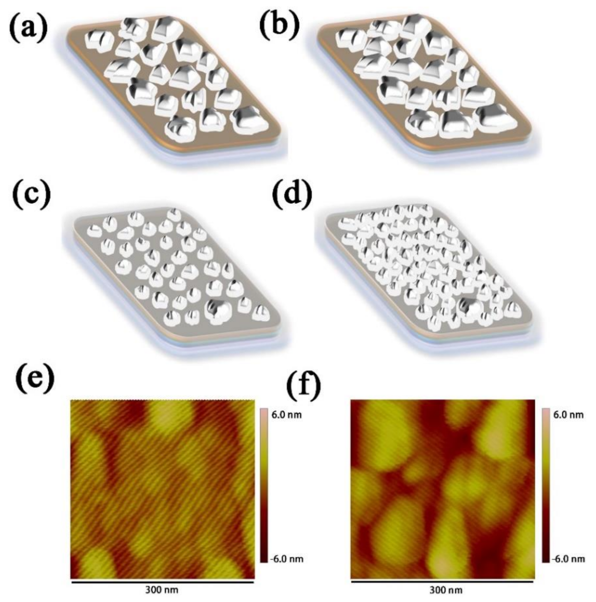
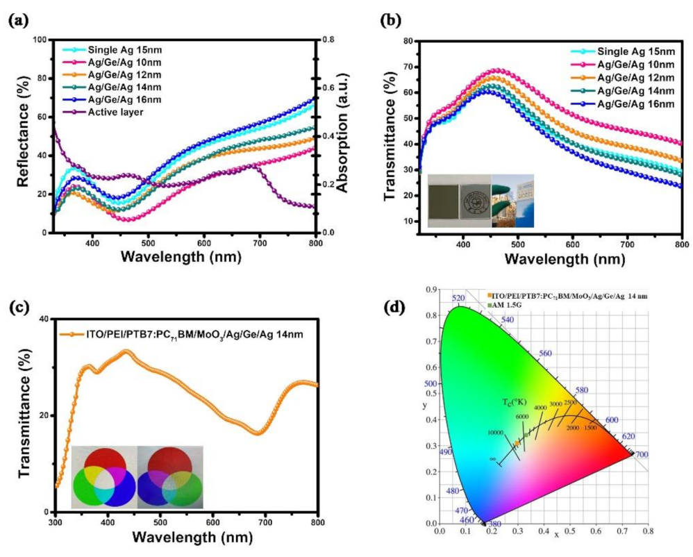
3. Result and Discussion
4. Conclusions
Supplementary Materials
Author Contributions
Funding
Data Availability Statement
Acknowledgments
Conflicts of Interest
References
- Dennler, G.; Scharber, M.C.; Brabec, C.J. Polymer-fullerene bulk-heterojunction solar cells. Adv. Mater. 2009, 21, 1323–1338. [Google Scholar] [CrossRef]
- Chen, X.; Jia, B.H.; Zhang, Y.A.; Gu, M. Exceeding the Limit of Plasmonic Light Trapping in Textured Screen-printed Solar Cells Using Al Nanoparticles and Wrinkle-like Graphene Sheets. Light Sci. Appl. 2013, 2, e92. [Google Scholar] [CrossRef] [Green Version]
- Tang, C.W. Two-layer organic photovoltaic cell. Appl. Phys. Lett. 1986, 48, 183–185. [Google Scholar] [CrossRef]
- Li, X.C.; Xie, F.X.; Zhang, S.Q.; Hou, J.H.; Choy, W.C. MoOx and V2Ox as Hole and Electron Transport Layers Through Functionalized Intercalation in Normal and Inverted Organic Optoelectronic Devices. Light Sci. Appl. 2015, 4, e273. [Google Scholar] [CrossRef] [Green Version]
- Zhang, Y.; Zhou, H.; Seifter, J.; Ying, L.; Mikhailovsky, A.; Heeger, A.J.; Bazan, G.C.; Nguyen, T.Q. Molecular Doping Enhances Photoconductivity in Polymer Bulk Heterojunction Solar Cells. Adv. Mater. 2013, 25, 7038–7044. [Google Scholar] [CrossRef] [PubMed]
- Guo, C.F.; Sun, T.S.; Cao, F.; Liu, Q.; Ren, Z. Metallic Nanostructures for Light Trapping in Energy-harvesting Devices. Light Sci. Appl. 2014, 3, e161. [Google Scholar]
- Park, B.; Yun, S.H.; Cho, C.Y.; Kim, Y.C.; Shin, J.C.; Jeon, H.G.; Huh, Y.H.; Hwang, I.; Baik, K.Y.; Lee, Y.I.; et al. Surface plasmon excitation in semitransparent inverted polymer photovoltaic devices and their applications as label-free optical sensors. Light Sci. Appl. 2014, 3, e222. [Google Scholar] [CrossRef]
- Lee, K.; Lee, J.; Mazor, B.A.; Forrest, S.R. Transforming the cost of solar-to-electrical energy conversion: Integrating thin-film GaAs solar cells with non-tracking mini-concentrators. Light Sci. Appl. 2015, 4, e288. [Google Scholar] [CrossRef] [Green Version]
- Zhong, Y.; Trinh, M.T.; Chen, R.; Purdum, G.E.; Khlyabich, P.P.; Sezen, M.; Oh, S.; Zhu, H.; Fowler, B.; Zhang, B.; et al. Molecular helices as electron acceptors in high-performance bulk heterojunction solar cells. Nat. Commun. 2015, 6, 1–8. [Google Scholar] [CrossRef] [PubMed] [Green Version]
- Su, Y.H.; Ke, Y.F.; Cai, S.L.; Yao, Q.Y. Surface Resonance of Layer-by-Layer Gold Nanoparticles Induced Photoelectric Current in Environmentally-friendly Plasmon-Sensitized Solar Cell. Light Sci. Appl. 2012, 1, e14. [Google Scholar] [CrossRef]
- Blum, O.; Shaked, N.T. Predication of photothermal phase signatures from arbitrary plasmonic nanoparticles and experimental verification. Light Sci. Appl. 2015, 4, e322. [Google Scholar] [CrossRef] [Green Version]
- Kosten, E.D.; Atwater, J.H.; Parsons, J.; Polman, A.H.; Atwater, A. Highly Efficient GaAs Solar Cells by Limiting Light Eemission Angle. Light Sci. Appl. 2013, 2, e45. [Google Scholar] [CrossRef]
- Huang, W.; Cheng, P.; Yang, Y.; Li, G.; Yang, Y. High-Performance Organic Bulk-Heterojunction Solar Cells Based on Multiple-Donor or Multiple-Acceptor Components. Adv. Mater. 2018, 30, 1705706. [Google Scholar] [CrossRef] [PubMed]
- Chen, H.-Y.; Hou, J.; Zhang, S.; Liang, Y.; Yang, G.; Yang, Y.; Yu, L.; Wu, Y.; Li, G. Polymer solar cells with enhanced open-circuit voltage and efficiency. Nat. Photonics 2009, 3, 649–653. [Google Scholar] [CrossRef]
- Deibel, C.; Dyakonov, V. Polymer-fullerene bulk heterojunction solar cells. Rep. Prog. Phys. 2010, 73, 096401. [Google Scholar] [CrossRef] [Green Version]
- Gilot, J.; Wienk, M.M.; Janssen, R.A.J. Optimizing Polymer Tandem Solar Cells. Adv. Mater. 2010, 22, E67–E71. [Google Scholar] [CrossRef] [PubMed]
- Hu, Z.H.; Wang, J.; Ma, X.L.; Gao, J.H.; Xu, C.Y.; Wang, X.L.; Zhang, X.L.; Wang, Z.; Zhang, F.J. Semitransparent organic solar cells exhibiting 13.02% efficiency and 20.2% average visible transmittance. J. Mater. Chem. A 2021, 9, 6797–6804. [Google Scholar] [CrossRef]
- Hu, Z.H.; Wang, Z.; An, Q.S.; Zhang, F.J. Semitransparent polymer solar cells with 12.37% efficiency and 18.6% average visible transmittance. Sci. Bull. 2020, 65, 131–137. [Google Scholar] [CrossRef] [Green Version]
- Hu, Z.H.; Wang, J.; Ma, X.L.; Gao, J.H.; Xu, C.Y.; Yang, K.X.; Wang, Z.; Zhang, J.; Zhang, F.J. A critical review on semitransparent organic solar cells. Nano Energy 2020, 78, 105376. [Google Scholar] [CrossRef]
- Sista, S.; Park, M.-H.; Hong, Z.; Wu, Y.; Hou, J.; Kwan, W.L.; Li, G.; Yang, Y. Highly efficient tandem polymer photovoltaic cells. Adv. Mater. 2010, 22, 380–383. [Google Scholar] [CrossRef] [PubMed]
- Chung, W.-S.; Lee, H.; Lee, W.; Ko, M.J.; Park, N.-G.; Ju, B.-K.; Kim, K. Solution processed polymer tandem cell utilizing organic layer coated nano-crystalline TiO2 as interlayer. Org. Electron. 2010, 11, 521–528. [Google Scholar] [CrossRef]
- Van De Groep, J.; Spinelli, P.; Polman, A. Transparent conducting silver nanowire networks. Nano Lett. 2012, 12, 3138–3144. [Google Scholar] [CrossRef] [PubMed]
- Li, G.; Chu, C.-W.; Shrotriya, V.; Huang, J.; Yang, Y. Efficient inverted polymer solar cells. Appl. Phys. Lett. 2006, 88, 253503. [Google Scholar] [CrossRef] [Green Version]
- Ng, G.-M.; Kietzke, E.L.; Kietzke, T.; Tan, L.-W.; Liew, P.-K.; Zhu, F. Optical enhancement in semitransparent polymer photovoltaic cells. Appl. Phys. Lett. 2007, 90, 103505. [Google Scholar] [CrossRef]
- Chen, F.-C.; Wu, J.-L.; Hsieh, K.-H.; Chen, W.-C.; Lee, S.-W. Polymer photovoltaic devices with highly transparent cathodes. Org. Electron. 2008, 9, 1132–1135. [Google Scholar] [CrossRef]
- Huang, J.; Li, G.; Yang, Y. A semi-transparent plastic solar cell fabricated by a lamination process. Adv. Mater. 2008, 20, 415–419. [Google Scholar] [CrossRef]
- Yim, J.H.; Joe, S.-Y.; Pang, C.; Lee, K.M.; Jeong, H.; Park, J.-Y.; Ahn, Y.H.; de Mello, J.C.; Lee, S. Fully solution-processed semitransparent organic solar cells with a silver nanowire cathode and a conducting polymer anode. ACS Nano 2014, 8, 2857–2863. [Google Scholar] [CrossRef]
- Yu, W.; Jia, X.; Long, Y.; Shen, L.; Liu, Y.; Guo, W.; Ruan, S. Highly efficient semitransparent polymer solar cells with color rendering index approaching 100 using one-dimensional photonic crystal. ACS Appl. Mater. Interfaces 2015, 7, 9920–9928. [Google Scholar] [CrossRef]
- Chen, C.-C.; Dou, L.; Zhu, R.; Chung, C.-H.; Song, T.-B.; Zheng, Y.B.; Hawks, S.; Li, G.; Weiss, P.S.; Yang, Y. Visibly transparent polymer solar cells produced by solution processing. ACS Nano 2012, 6, 7185–7190. [Google Scholar] [CrossRef]
- Cioarec, C.; Melpignano, P.; Gherardi, N.; Clergereaux, R.; Villeneuve, C. Ultrasmooth silver thin film electrodes with high polar liquid wettability for OLED microcavity application. Langmuir 2011, 27, 3611–3617. [Google Scholar] [CrossRef]
- Melpignano, P.; Cioarec, C.; Clergereaux, R.; Gherardi, N.; Villeneuve, C.; Datas, L. E-beam deposited ultra-smooth silver thin film on glass with different nucleation layers: An optimization study for OLED micro-cavity application. Org. Electron. 2010, 11, 1111–1119. [Google Scholar] [CrossRef]
- Liu, S.; Liu, W.; Yu, J.; Zhang, W.; Zhang, L.; Wen, X.; Yin, Y.; Xie, W. Silver/germanium/silver: An effective transparent electrode for flexible organic light-emitting devices. J. Mater. Chem. C 2014, 2, 835–840. [Google Scholar] [CrossRef]
- Xia, R.; Brabec, C.J.; Yip, H.-L.; Cao, Y. High-throughput optical screening for efficient semitransparent organic solar cells. Joule 2019, 3, 2241–2254. [Google Scholar] [CrossRef]
- Li, Z.; Zhang, X.; Liu, C.; Zhang, Z.; He, Y.; Li, J.; Shen, L.; Guo, W.; Ruan, S. The performance enhancement of polymer solar cells by introducing cadmium-free quantum dots. J. Phys. Chem. C 2015, 119, 26747–26752. [Google Scholar] [CrossRef]
- Kang, T.S.; Chun, K.H.; Hong, J.S.; Moon, S.H.; Kim, K.J. Enhanced stability of photocurrent-voltage curves in Ru (II)-dye-sensitized nanocrystalline TiO2 electrodes with carboxylic acids. J. Electrochem. Soc. 2000, 147, 3049. [Google Scholar] [CrossRef]
- Ahmed, R.T. Obtaining and analyzing the characteristics curves of a solar cell. IJOCAAS 2017, 2, 94–98. [Google Scholar] [CrossRef]
- Moliton, A.; Nunzi, J.-M. How to model the behaviour of organic photovoltaic cells. Polym. Int. 2006, 55, 583–600. [Google Scholar] [CrossRef]
- Bahmani, E.; Zakeri, A.; Aghdam, A. Microstructural analysis and surface studies on Ag-Ge alloy coatings prepared by electrodeposition technique. J. Mater. Sci. 2021, 56, 6427–6447. [Google Scholar] [CrossRef]
- Brenner, A. Electrodeposition of Alloys: Principles and Practice; Elsevier: Amsterdam, The Netherlands, 2013. [Google Scholar]
- Kumaraguru, S.; Pavulraj, R.; Vijayakumar, J.; Mohan, S. Electrodeposition of cobalt/silver multilayers from deep eutectic solvent and their giant magnetoresistance. J. Alloy. Compd. 2017, 693, 1143–1149. [Google Scholar] [CrossRef]
- Łukaszewski, M.; Klimek, K.; Czerwiński, A. Microscopic, spectroscopic and electrochemical characterization of the surface of Pd–Ag alloys. J. Electroanal. Chem. 2009, 637, 13–20. [Google Scholar] [CrossRef]
- Tai, C.; Su, F.; Sun, I. Electrodeposition of palladium–silver in a Lewis basic 1-ethyl-3-methylimidazolium chloride-tetrafluoroborate ionic liquid. Electrochim. Acta 2005, 50, 5504–5509. [Google Scholar] [CrossRef]
- Sun, G.; Shahid, M.; Fei, Z.; Xu, S.; Eisner, F.D.; Anthopolous, T.D.; McLachlan, M.A.; Heeney, M. Highly-efficient semi-transparent organic solar cells utilizing non-fullerene acceptors with optimized multilayer MoO3/Ag/MoO3 electrodes. Mater. Chem. Front. 2019, 3, 450–455. [Google Scholar] [CrossRef]
- Xu, G.; Shen, L.; Cui, C.; Wen, S.; Xue, R.; Chen, W.; Chen, H.; Zhang, J.; Li, H.; Li, Y.; et al. High performance colorful semitransparent polymer solar cells with ultrathin hybrid-metal electrodes and fine-tuned dielectric mirrors. Adv. Funct. Mater. 2017, 27, 1605908. [Google Scholar] [CrossRef]


| Device (nm) | Illumination | JSC (mA/cm2) | VOC (V) | FF (%) | PCE (%) |
|---|---|---|---|---|---|
| Single Ag 15 | Bottom | 10.07 | 0.673 | 56 | 3.8 |
| Single Ag 15 | Top | 1.96 | 0.626 | 58 | 0.7 |
| Ag/Ge/Ag 10 | Bottom | 10.16 | 0.688 | 62 | 4.3 |
| Ag/Ge/Ag 10 | Top | 2.39 | 0.651 | 62 | 1.0 |
| Ag/Ge/Ag 12 | Bottom | 11.18 | 0.686 | 61 | 4.7 |
| Ag/Ge/Ag 12 | Top | 2.51 | 0.654 | 61 | 1.0 |
| Ag/Ge/Ag 14 | Bottom | 11.63 | 0.703 | 63 | 5.1 |
| Ag/Ge/Ag 14 | Top | 2.27 | 0.659 | 66 | 1.0 |
| Ag/Ge/Ag 16 | Bottom | 11.75 | 0.702 | 62 | 5.1 |
| Ag/Ge/Ag 16 | Top | 2.04 | 0.660 | 69 | 1.0 |
Publisher’s Note: MDPI stays neutral with regard to jurisdictional claims in published maps and institutional affiliations. |
© 2021 by the authors. Licensee MDPI, Basel, Switzerland. This article is an open access article distributed under the terms and conditions of the Creative Commons Attribution (CC BY) license (https://creativecommons.org/licenses/by/4.0/).
Share and Cite
Guo, J.; Bu, Z.; Han, S.; Deng, Y.; Liu, C.; Guo, W. Easily Prepared Transparent Electrodes for Low-Cost Semitransparent Inverted Polymer Solar Cells. Energies 2021, 14, 5837. https://doi.org/10.3390/en14185837
Guo J, Bu Z, Han S, Deng Y, Liu C, Guo W. Easily Prepared Transparent Electrodes for Low-Cost Semitransparent Inverted Polymer Solar Cells. Energies. 2021; 14(18):5837. https://doi.org/10.3390/en14185837
Chicago/Turabian StyleGuo, Jiaxin, Ziming Bu, Shuo Han, Yanyu Deng, Chunyu Liu, and Wenbin Guo. 2021. "Easily Prepared Transparent Electrodes for Low-Cost Semitransparent Inverted Polymer Solar Cells" Energies 14, no. 18: 5837. https://doi.org/10.3390/en14185837