1. Introduction
In the last few decades, energy harvesting from renewable energy sources has been growing rapidly, as a result of increased fossil fuel costs and increased power demand. However, the growing environmental problems are a serious concern in our society, which must not be neglected. Solar and wind energy are the two types of renewable energy sources that concentrate the biggest interest for clean energy generation. More specific, solar energy is gaining more and more attention and the photovoltaic (PV) power injection to the utility grid is growing, since it offers many advantages, such as [
1,
2]:
Solar energy is a non-exhaustible energy source.
PV cells now offer increased power conversion efficiency and low cost.
Energy conversion can be achieved without extra pollution.
PV cells produce maximum power during midday, when the power demand reaches its peak value.
For all these reasons, large-scale, high-power PV plants are being implemented, ranging from tens of kilowatts up to several megawatts [
2]. Although PV plant technology is growing rapidly, there are some problems that can cause severe power loss. The most common problems reported in PV plants (at the PV panel level) are the hot spots on the PV panels and the potential induced degradation (PID) effect [
3].
By the term hot spot, we refer to the PV cells within the PV panel, which are characterized by an increased temperature value. The main reasons that can cause hot spots in PV panels are the mismatched PV cells’ electrical characteristics, the partial shadowing of the panel and the microcracks. When n series-connected cells supply a load while one or more cells are damaged (or shadowed), they consume a part of the generated power. The power consumed by the faulty cells is converted to heat, causing a rise in their temperature. This power loss can be limited in practice by connecting bypass diodes in parallel from twelve to twenty-four cells [
4].
Another problem that can affect the power generated from PV panels is the PID effect, where the energy generated from a PV plant is decreased when the PID effect is present [
4,
5]. This problem is caused to PV panels, which are feeding the grid with active power, by using non-isolated inverters. The eliciting factor of the PID effect is the high voltage difference between the PV cell and the aluminium frame of the PV panel, due to the high number of series-connected panels and the inability of earth-grounding one of the output terminals of the string [
6,
7]. The presence of a strong electric field between the PV cell and the aluminium frame, which is earth-grounded, causes an electron leakage [
8,
9]. This phenomenon can be recognized either by the thermal imaging of the PV panel or by measuring its electrical values (voltage and current) under load. From the literature, it is deduced that the PID effect is a reversible phenomenon if it is diagnosed and treated in its first stages [
10]. Nonetheless, there are cases where the PID effect may cause irreversible damage to the PV panel, as presented in [
11].
To deal with the degradation of PV panels, various methods have been proposed, some related to the prevention of the PID phenomenon, while others to revert its effects. The PID appears in PV arrays where there is an inability to connect the negative or positive pole of the array (depending on the cell type) to the earth-ground. Therefore, the use of electronic devices that allow the earth-grounding of the PV panel is a good solution that can be applied in advance when building a PV unit. For example, power converters with galvanic isolation [
12] or advanced converters without isolation that allow the PV panel terminals to be earth-grounded [
13] are ways to prevent the degradation. This, however, requires particular system specifications and is not always feasible. On the other hand, at the microscopic level, an alternative way to prevent the PID is to use specific PV cells and frames (glass surface, anti-reflective coating, etc.) that have a special molecular structure, with the advantage that they do not leak e- or they have a significantly reduced leakage current [
14,
15]. This solution, like the previous one, may have limitations and increased cost in case of replacement of the existing units in a photovoltaic park. Thermal recovery is another way to solve the PID problem [
10]. Storing PID-affected PV panels in chambers with a temperature around 100 °C leads to the recovery of the PV panel, but it causes high stress on the panel materials, which may affect their overall lifetime. The subjection of the PID-affected panel to UV exposure reverses the phenomenon. Both solutions require special infrastructure. Another method for solving the PID phenomenon is the biasing of the PV cells with a high voltage, with a polarity opposite to the voltage causing the phenomenon. Specifically, a high voltage can be applied between the cell and the frame [
16] or by using corona discharge [
10,
17]. Commercial products, such as in [
18,
19,
20], apply high voltage to PV panels to deal with PID problems that already exist, but the complexity of their power conversion stage is unknown. However, to the best knowledge of the authors, there is no specific power electronics converter solution described in the literature for the given application.
In this paper, a comprehensive solution for regenerating PV cells affected by PID is proposed. A simple and low cost high step-up power electronics converter, based on the Cockroft–Walton voltage multiplier, is implemented, with the ability to treat and artificially create PID for research purposes. The converter can provide a four-step variable DC voltage, which is useful for research purposes when the rate of the PID effect development is investigated. Moreover, with a portable plug-and-play device, compatible with communication protocols, the PID effect can be studied without the relocation of the PV panels. The rest of the paper is organized as follows. In
Section 2, the operational principals of the PID and the proposed regenerative method are presented. In
Section 3, the power converter, deployed for the high voltage generation, is analyzed, along with all the power conversion stages. In
Section 4, the experimental validation of the implemented device is presented in a standalone operation and with actual PV panels.
Section 5 concludes the paper.
2. Regeneration of Photovoltaic Cells
In this section, a simple and comprehensive explanation of the PID effect is given. As already described in Section I, PID is a reversable phenomenon and there are different methods to encounter it. The suggested method is by utilizing a power converter that can be externally connected to multiple PV panels, even if they are already installed in a photovoltaic park. By regenerating the PV cells, the maximum output power is increased, by restoring the open circuit voltage, the short-circuit current and the maximum power point (MPP), close to their nominal values.
2.1. Potential Induced Degradation on p-Type & n-Type Cells
The PV cells that make up a PV panel are divided into two categories depending on their structure. Based on the type of semiconductor used as a base for their construction, a PV panel can be either p-type or n-type. The PID effect occurs in both cases but under different conditions [
9]. Therefore, it is necessary to either know the structure of the cells or to be able to determine it experimentally, as will be analyzed below.
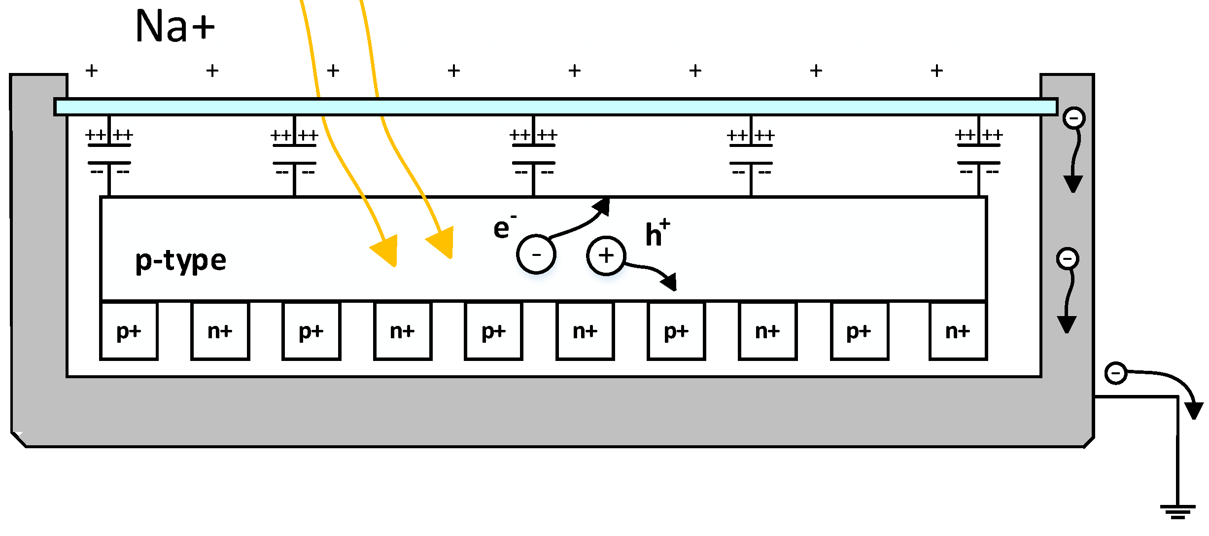
During normal operation, the electrons accelerate towards the n+ region, under the influence of the potential barrier between the p-n contact and the holes towards the p+ region. In
Figure 1, the cross-section of a p-type PV panel is illustrated. The group of cells are supported on an aluminum base and covered by a glass surface and an anti-reflective coating, which reduces the reflected radiation. The PID effect occurs when a positive charge, such as sodium cations (Na
+), settle on the glass surface. Photons produced by solar irradiation fall on the p-type semiconductor of the cell, creating holes (h
+) and electrons (e
−). In the event that a positive charge has accumulated on the surface (e.g., silicon dioxide (SiO
2)) and on the anti-reflective coating (e.g., silicon nitride (Si
3N
4)), the electrons are attracted to the glass surface, or otherwise the holes are directed to the p
+ region. Charge accumulation can be represented by equivalent capacitors between the cells and the glass [
21], as shown in
Figure 1. As a result, there is leakage of electrons to the earth-ground, meaning that the conventional direction of the current is from the earth-ground towards the frames. As a consequence, a negative potential difference between the cells and earth-ground is developed [
9]. This bias effect is intensified by high humidity, which reduces the impedance between the glass surface and the aluminum support frame, increasing the leakage current. The aluminum frame is naturally connected to the earth-ground. The cells that are most affected by this phenomenon are those closest to the negative pole of the DC voltage, where the voltage potential with respect to the earth-ground is higher [
4,
5].
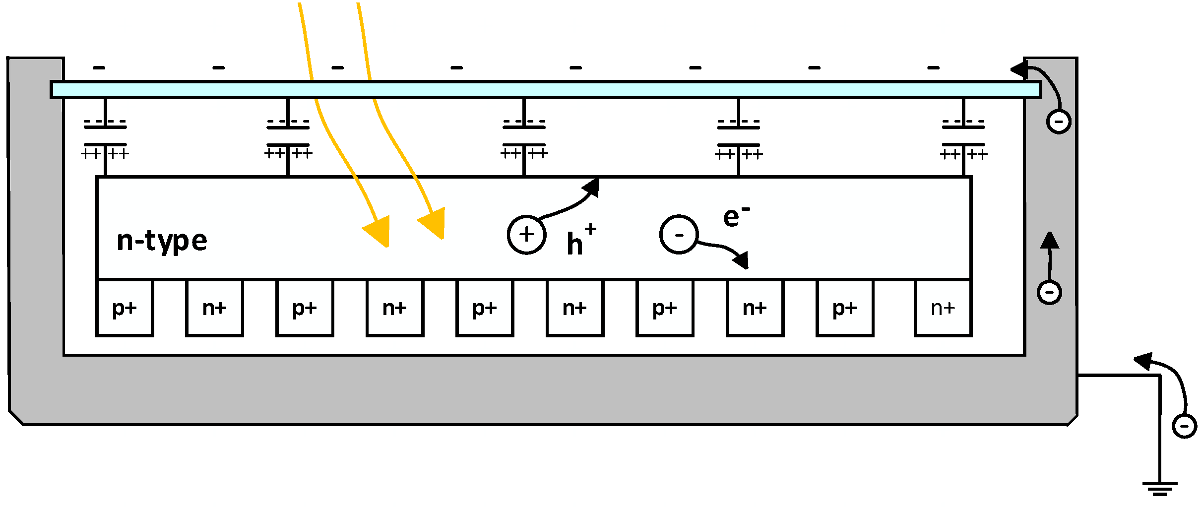
If the PV cells are constructed with n-type semiconductors, the occurrence of the PID phenomenon is similar with the p-type cells that was previously described. In
Figure 2, a representative example is shown, where a negative charge has accumulated on the glass surface, creating a parasitic capacitance. A positive potential with respect to the earth-ground is now present. As shown in
Figure 2, the leakage is opposite to the previous case and the phenomenon is more intense at the cells towards the positive pole of the output voltage [
9].
In any case, by short-circuiting the output of the PV panels, it is possible to detect the potential difference by measuring the voltage between this common point with the aluminum support frame. In this way the cell type is identified.
2.2. Regeneration with a Power Converter
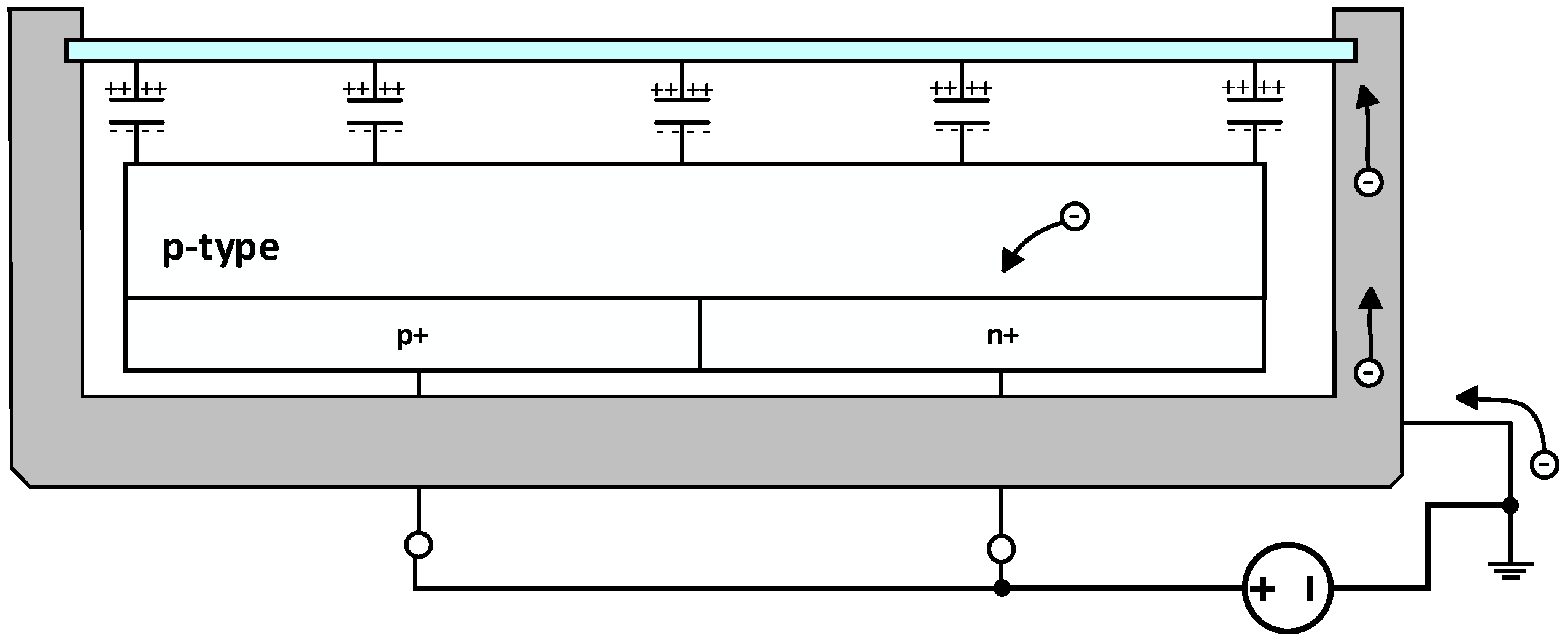
As mentioned earlier, the reverse of PID effect can be achieved with the use of a power electronics converter. A high DC voltage is applied between the PV panel output and the aluminum support frame, which is directly connected to the earth-ground, as shown in
Figure 3. The polarity of the voltage is the opposite of that which causes the degradation phenomenon. This way, the potential of the PV panel relative to the earth-ground is raised, and the leakage current is eliminated by reversing the flow of electrons back to the PV cells. The voltage amplitude should not exceed the maximum system voltage, as defined by the manufacturer of the PV panel. The device can operate when there is no energy production, either during the night or if the panels are manually and totally shaded [
17]. The regeneration process even can be speeded-up, if the glass surface is damp, since the impedance of the escape path of the e- is reduced [
9].
Our goal is not only to reverse the PID effect on the panels, but also to create a device that can be installed easily and at any environment, that can be applied to any type of cells (p-type or n-type), and that is simple and safe to use. In a PV park, the outputs of the PV array are short-circuited during the regeneration, while the main inverter is disconnected from the grid.
The PID effect on p-type cells does not occur when the voltage applied by the converter is positive. Therefore, there is no risk of causing any damage to the PV panels due to prolonged polarization of the array. This automatically provides safety to the system and reduces the complexity of the power converter control. The converter can be connected to multiple PV arrays that are parallelly connected, so that they are polarized with the same voltage.
2.3. Artificial Creation of PID on PV Panels
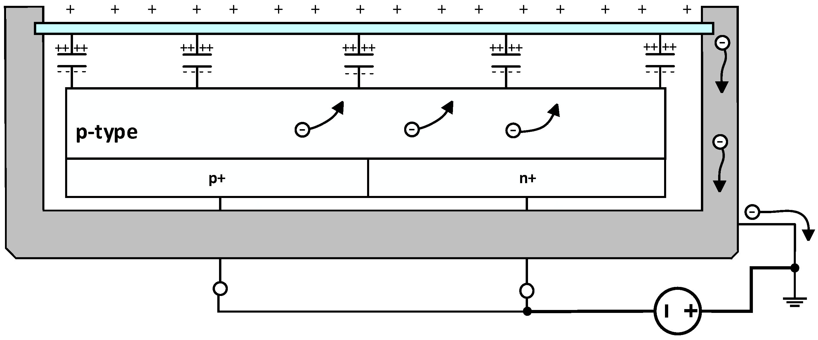
As already mentioned, the PID phenomenon is evolving slowly and its effects are becoming apparent in the long run. To study the problem and analyze the effects and the damages it causes on PV panels, an easy method to artificially create PID on PV panels under controlled conditions is proposed. By utilizing the same power converter that is used for the regeneration of the PV cells and reversing the output voltage, the electric field that causes the leakage of electrons is applied to the panel. In
Figure 4, an example of artificially creating PID is depicted, where the power converter is connected in reverse, compared to
Figure 3, and the flow of electrons is forced in such a direction so as to degrade the PV cells. A positive charge has accumulated on the glass surface as a result, just like the naturally occurring phenomenon shown in
Figure 1.
Compared to the other solutions mentioned in
Section 1, the proposed method offers many advantages: not only it is a low cost solution, but, also, there is no need for special equipment to generate a high voltage and place cations on the glass surface; the device is portable and can be tested anywhere, by simply shading the panel surface; and multiple panels can be connected in parallel or in series for mass testing.
3. Power Converter Description
The main requirements of the power electronics converter in this application is to produce a high DC voltage at light load conditions (due to the low leakage currents), the ability to use low rating semiconductor devices to cut down the cost and to simplify the control of the output voltage. What is more, since high accuracy of the converter output voltage level is not a strict requirement, the converter is designed to generate four discrete voltage levels. As the device features a plug-and-play operation, a pre-charge circuit is used for the start-up when the mains utility voltage of 230 V/50 Hz is connected. The galvanic isolation is also a requirement to prevent unexpected short circuits, since the neutral of the power distribution network and the DC output of the converter are both earth-grounded.
The power converter used for generating a high DC voltage is based on the Cockroft–Walton voltage multiplier (CW-VM). The CW-VM topology is selected for this application, since it offers many advantages, such as the use of semiconductor devices and capacitors with low ratings, since the maximum theoretical voltage of the switching devices and the capacitors is equal to the double of the peak input voltage at the worst-case scenario.
The voltage gain of the CW-VM with n stages can be calculated by (1) (without load), in which
Epk is the peak value of the input voltage and
Vo,nl is the mean value of the non-loaded output voltage [
22]. In this application, the output current of the converter does not exceed the magnitude of some mA (or less); therefore, the voltage drop of the output can be neglected. Even more, due to the nature of the application, there are no abrupt changes in the load that can affect the converter output voltage.
As described in [
22], a voltage ripple across the capacitors of the topology is present under load. This voltage ripple can be very high if the frequency of the AC voltage source supplying the CW-VM is low. Taking into consideration that the utility grid has a frequency equal to 50 Hz, there are two solutions for limiting the voltage ripple. The obvious solution is to increase the total capacitance of the CW-VM, and the second solution is to feed the voltage multiplier with a high frequency AC voltage. In this paper, the second solution is adopted to decrease the total volume of the device. To do so, a Half-Bridge inverter is used to produce the high frequency AC voltage required [
23]. The significant advantage of the proposed topology is the simplicity of the control. Specifically, the frequency and the duty cycle of the Half-Bridge are kept constant and the adjustment of the output voltage is implemented using a relay network connected to the CW-VM outputs.
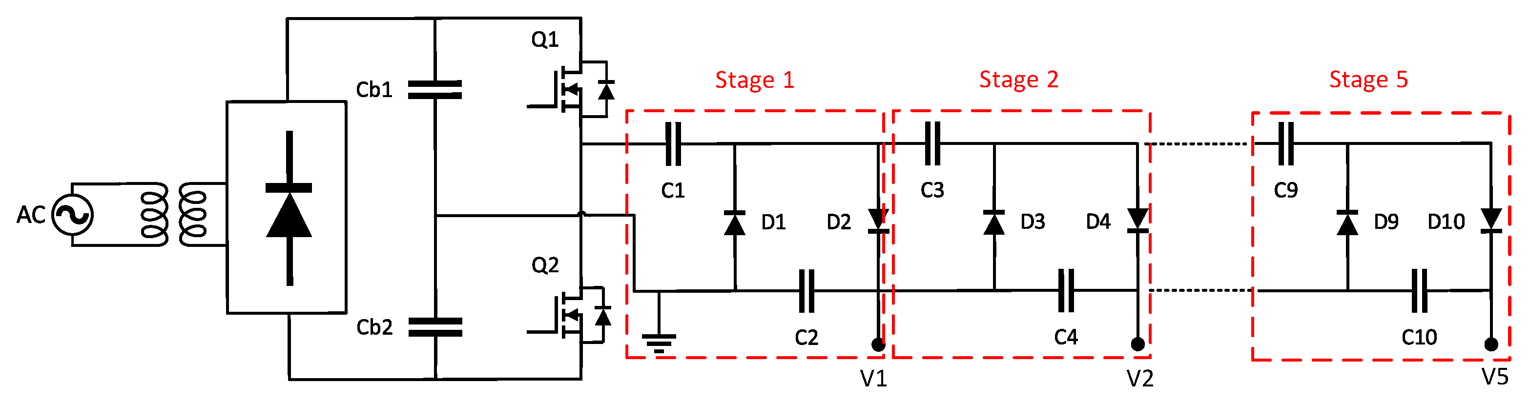
Specifically, the mains voltage is stepped down with the use of a transformer to provide a 144 V/50 Hz voltage. Then, a rectifier with filtering capacitors is used to produce a smooth DC voltage for the DC/AC conversion stage. The final power conversion stage is the voltage multiplication stage. The stepped down voltage is necessary for the CW-VM to produce five different voltage levels at the output, ranging from approximately 200 V to 1000 V, with steps of 200 V. The output voltage level can be selected by controlling the state of the relays connected at the output of Stage 2–Stage 5 of the CW-VM. The total converter topology is depicted in
Figure 5.
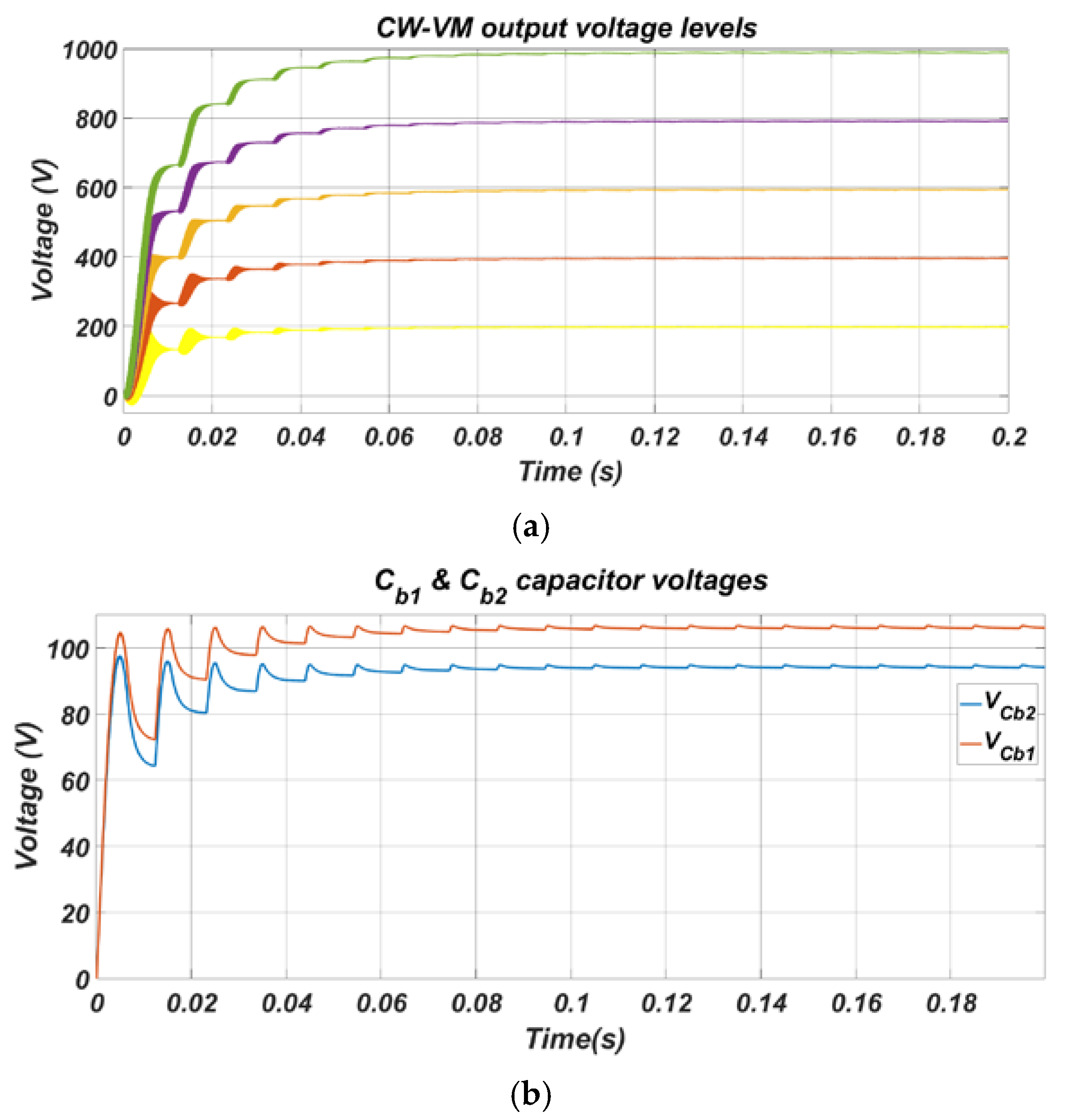
To verify the operation of the proposed converter, some indicative simulation results are presented in
Figure 6a,b. The Half-Bridge capacitances were chosen solely based on the desired voltage ripple
Cb1 =
Cb2 = 94 μF and each CW-VM capacitance
Ci (i = 1,2,..,10) is equal to 12 μF, with the load current been equal to 5 mA. The semiconductor switches
Q1 and
Q2 are controlled with complementary pulses with a frequency of 20 kHz.
As can be seen from
Figure 6a, a small voltage drop is noticeable due to the operational properties of the CW-VM compared to (1) [
22]. What is more, from
Figure 6b is deduced that the voltages across the capacitors
Cb1 and
Cb2 are not equal. This can be easily explained if the single stage CW-VM topology is considered. When the
Q2 transistor is ON, the capacitor
Cb2 is connected in parallel with capacitor
C1. In the time interval in which the
Q1 transistor is ON, the capacitor
Cb1 is in parallel with the series connection of capacitors
C1 and
C2. Following a similar logic, it can be deduced that the effective capacitance at the positive half-cycle of the DC/AC stage is smaller compared to the effective capacitance of a negative half-cycle. Hence, the voltage across capacitor
Cb2 is lower.
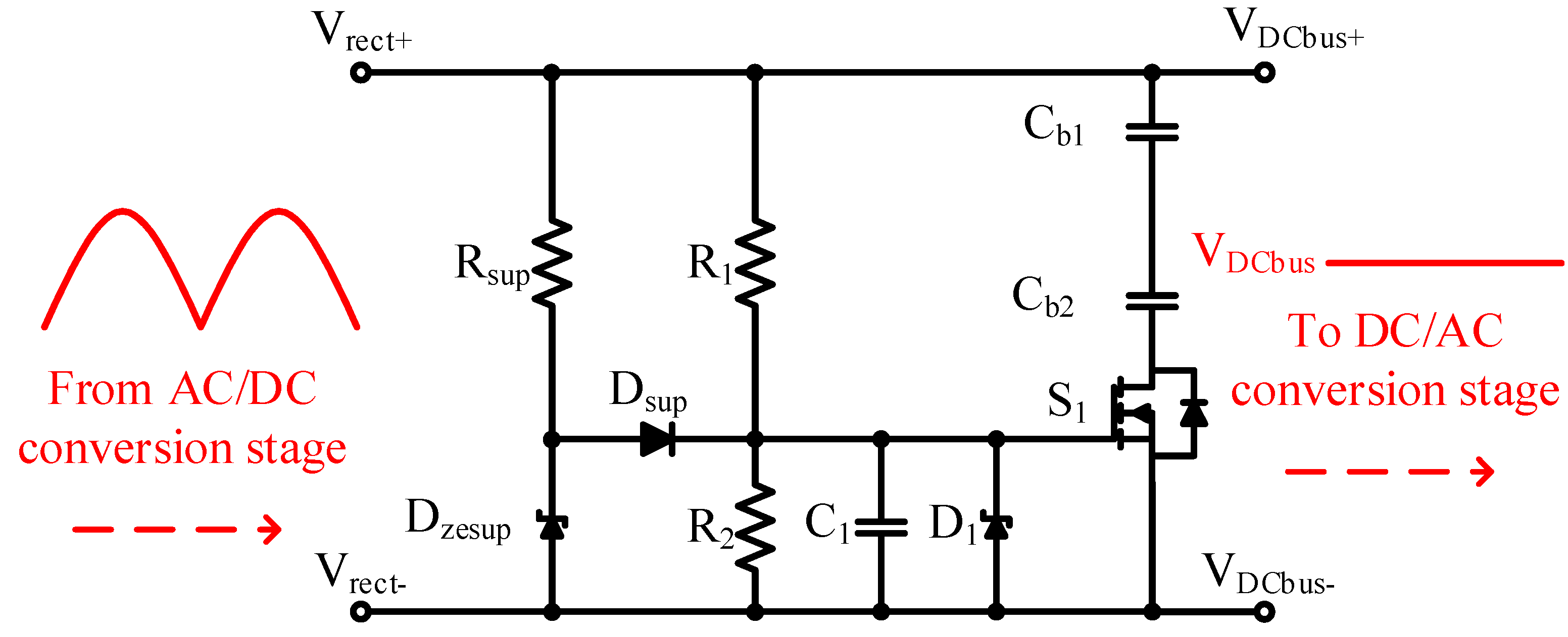
As described, the power electronics converter is designed to be supplied by the utility grid (230 V/50 Hz). For long-term and reliable operation, the electrolytic capacitors at the output of the rectifier must be soft charged to limit the high inrush current. There are several ways to provide a soft charging for the smoothing capacitors. The pre-charge circuit used in our application is depicted in
Figure 7, which is an improved version of the pre-charge circuit reported in [
24], to speed up the initial charging process of the capacitors
Cb1 and
Cb2, especially for cases where the input voltage comes from the rectified mains voltage. The
CDCbus capacitor is the series combination of
Cb1 and
Cb2.
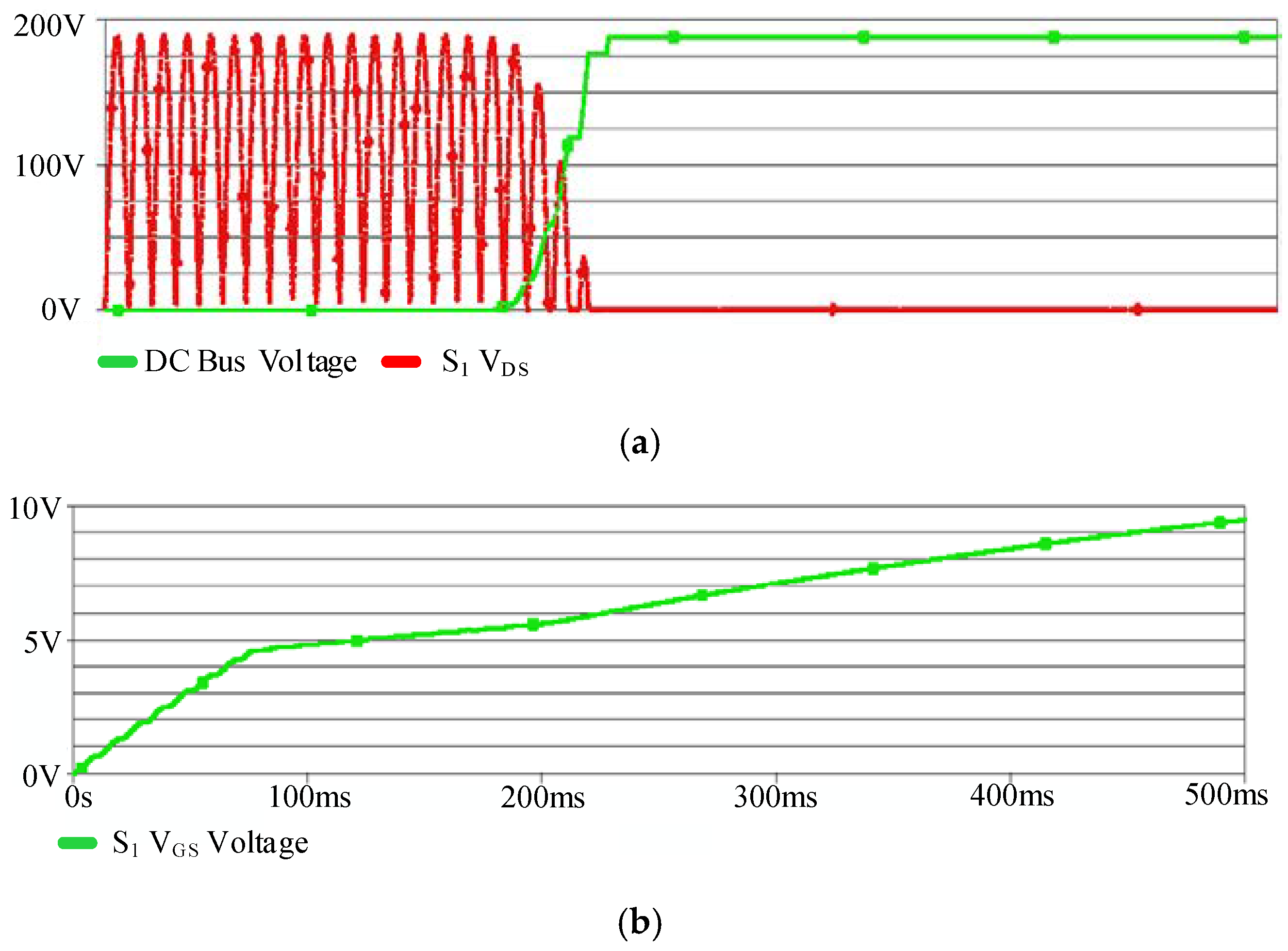
The simulation results of the pre-charge circuit are shown in
Figure 8. Specifically, in
Figure 8a, the DC bus voltage along with the drain-source voltage
VDS of the
S1 transistor are shown, whereas in
Figure 8b the gate-source voltage
VGS of the transistor is presented. The effects of the additional circuitry (
Rsup,
Dsup, and
Dzesup) can been noticeable up to 80 ms, where the
S1 gate-source is speeded-up, up to a value close but below the transistor threshold voltage.
4. Experimental Validation
The proposed power converter was implemented and tested on real photovoltaic panels, in order to validate both the artificial creation of the PID phenomenon and the regeneration of the PV cells. It is a plug-and-play device, with output voltage and current measurements as well as overvoltage and overcurrent protection features. First, the device was tested separately, to verify its operation and its plug-and-play capability. Next, the PID phenomenon was artificially created on one PV panel, while another healthy one was used as the “control panel”, serving as a reference point for comparison before and after the PID. After degrading the PV cells of the selected panel for 2 weeks, the regeneration process followed for the same time period. Measurements of the characteristic P-V and I-V curves of both panels were taken along the process. The durability and the operational principles of the device were successfully verified.
4.1. Experimental Prototype
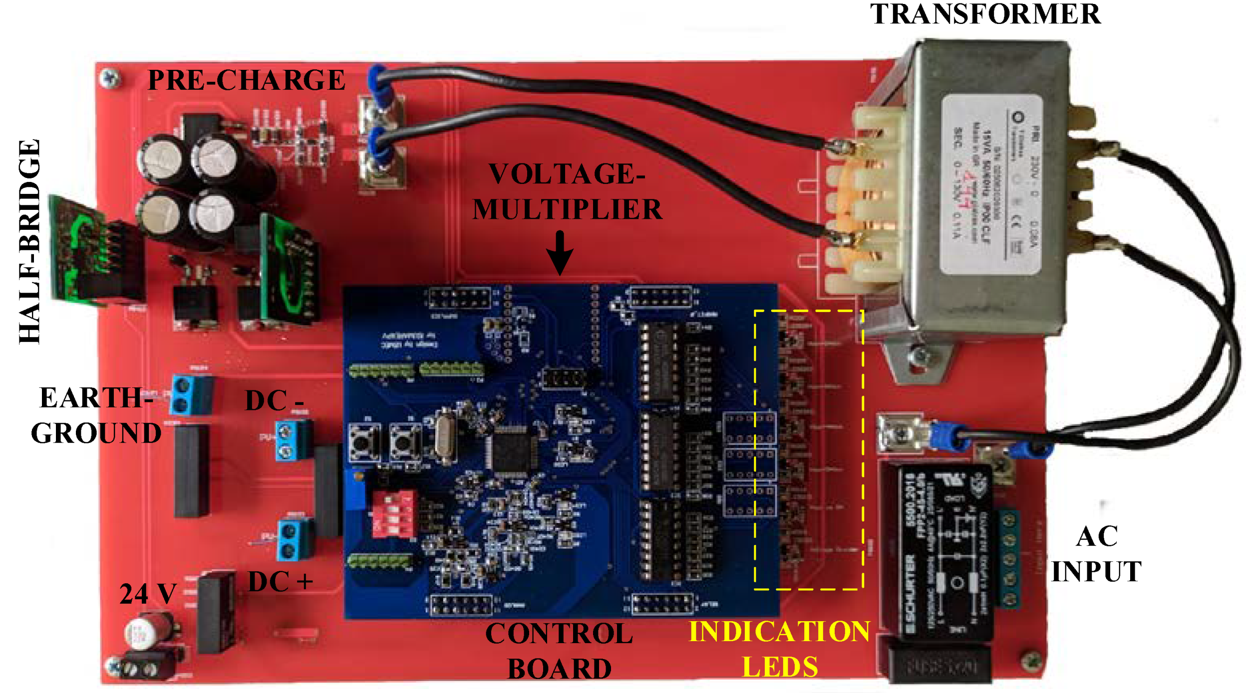
An experimental prototype device based on the Cockroft–Walton voltage multiplier topology was designed and implemented. In
Figure 9, the power circuit (red PCB) and the control board (blue PCB) are shown. The detailed characteristics of the power converter are given in
Table 1. The different stages of the output voltage make this device adaptable in a wide variety of systems with different characteristics.
The desired output is selected via a DIP-switch and the active output stage (Vo,2, Vo,3, Vo,4, Vo,5) is indicated with on-board LEDs when the corresponding relay is closed. There are also LEDs that indicate when the relays, which short-circuit the PV terminals PV+ with PV-, and the voltage measurement divider are turned on. The latter is very important, because if the device is constantly connected to the PV panel, it can monitor the reverse voltage that is caused due to the PID effect between the PV- and the earth-ground. However, the voltage divider placed between these terminals for measuring causes additional leakage when the PV cells are not regenerated, enhancing the leakage of electrons. Therefore, when only monitoring the PV panel and the power circuit is off, the voltage of the PV with respect to earth-ground is discontinuously sampled by switching on and off the corresponding relay, instead of constantly measuring it. The output current was also measured; however, its value is extremely small, since the output impedance is very high and mainly of capacitive nature. Despite that, both voltage and current measurements were obtained during operation and send via UART communication to a computer for evaluation.
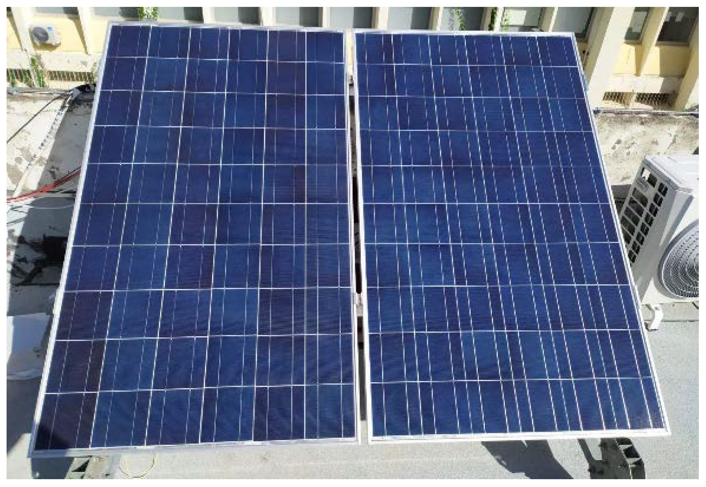
Two almost identical and healthy/undamaged PV panels were used in the experiments. In
Table 2, the detailed ratings of each panel are given. The second panel PV
2, which has slightly higher characteristics in power, voltage and current, was selected as the test subject for the PID phenomenon. This was chosen to ensure that any degradation of the electrical characteristics of its output, compared to the “control panel” PV
1, would be due to the PID effects. In
Figure 10, the experimental setup of the PV panels installed on the rooftop of our laboratory is shown. The PV panels were shaded during the artificial creation of the PID phenomenon and when regenerating the PV cells. The PID device was enclosed in a waterproof box to be protected while being installed under the PV panels.
4.2. Experimental Results
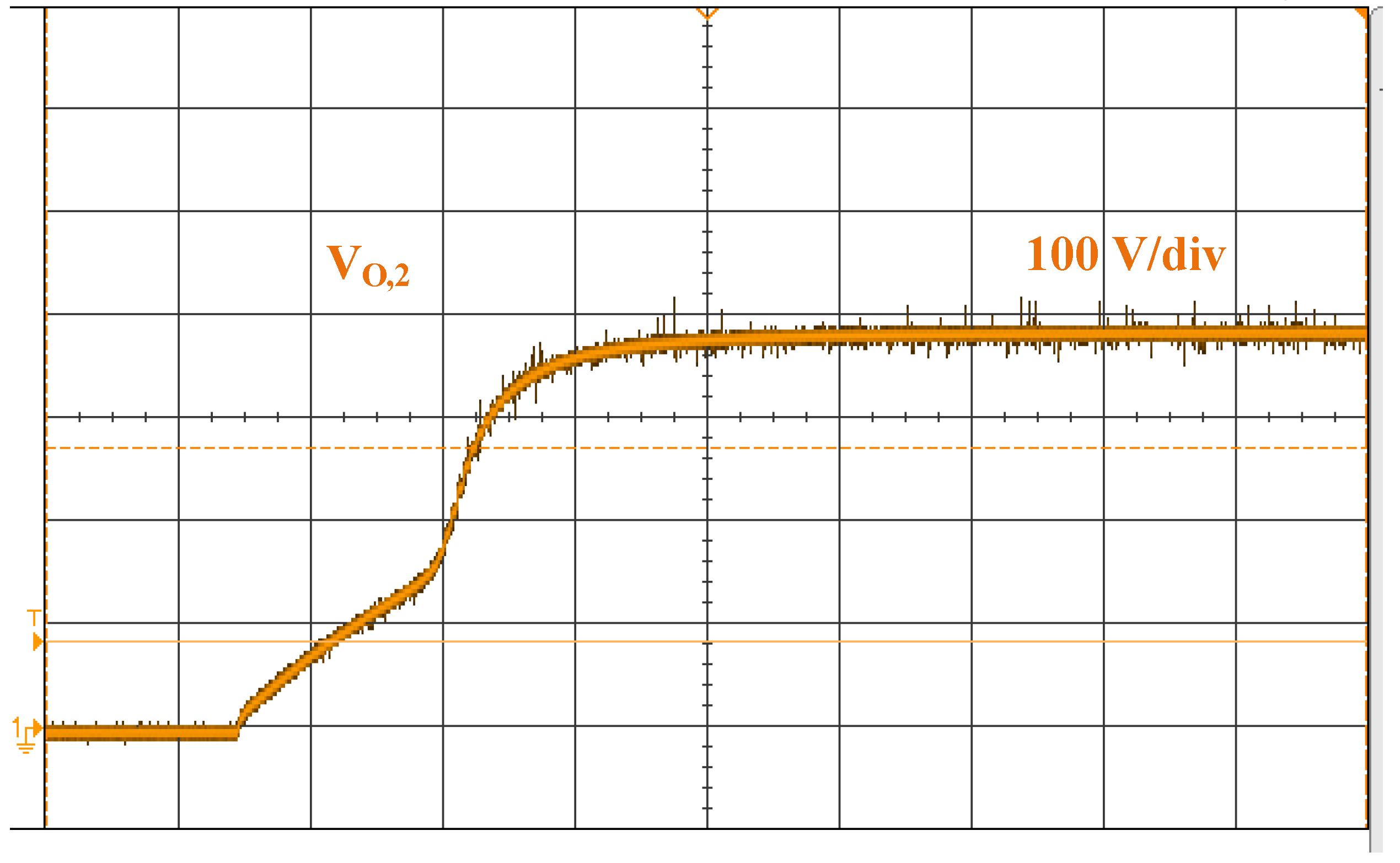
First, the converter was tested in a laboratory environment, to examine its behavior during start-up, as well as in the steady-state operating point. In
Figure 11, the input DC bus capacitors voltage
VC,DCbus is depicted, along with the DC bus voltage, during start-up. The effectiveness of the pre-charge circuit is verified, and a gradual charging of the capacitors is accomplished. As can be seen from
Figure 11, the MOSFET used for the pre-charge initially is in the cut-off state; then, as the DC capacitor voltage is raised, the MOSFET enters the saturation region; and finally, when the DC bus capacitors are fully charged, MOSFET enters the linear region. Moreover, in
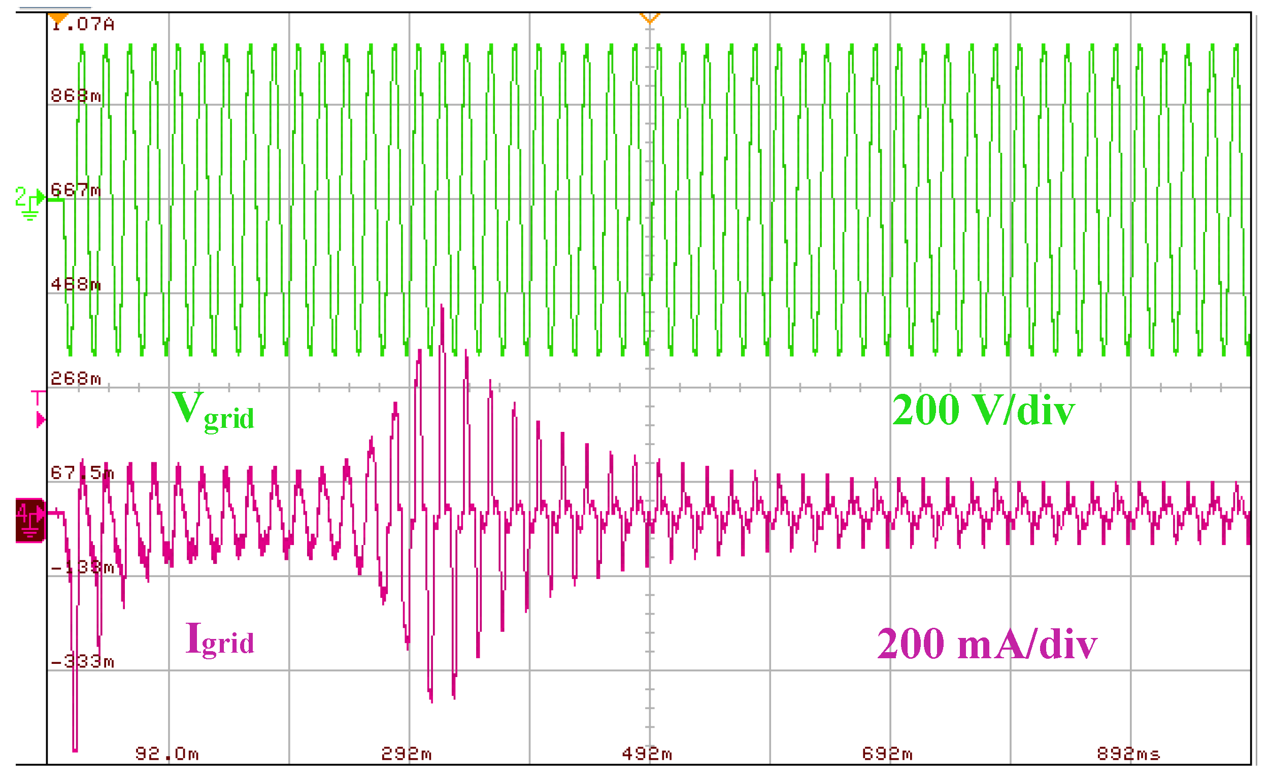
Figure 12, the input current of the grid-side is depicted, when plugging the device into the grid and no significant current overshoot is noted. In
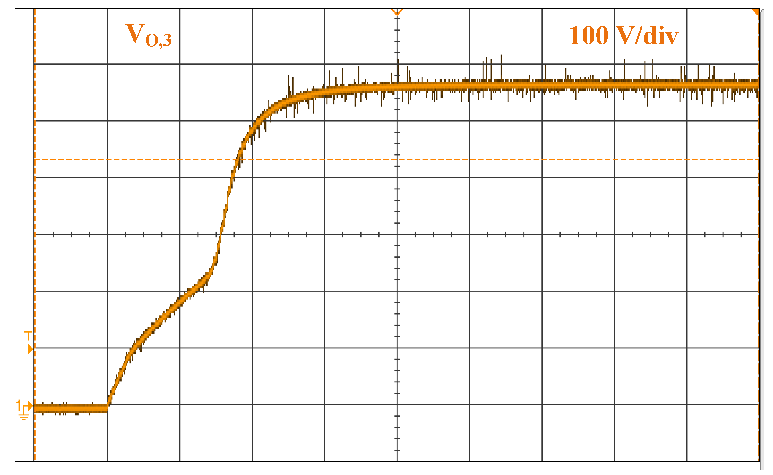
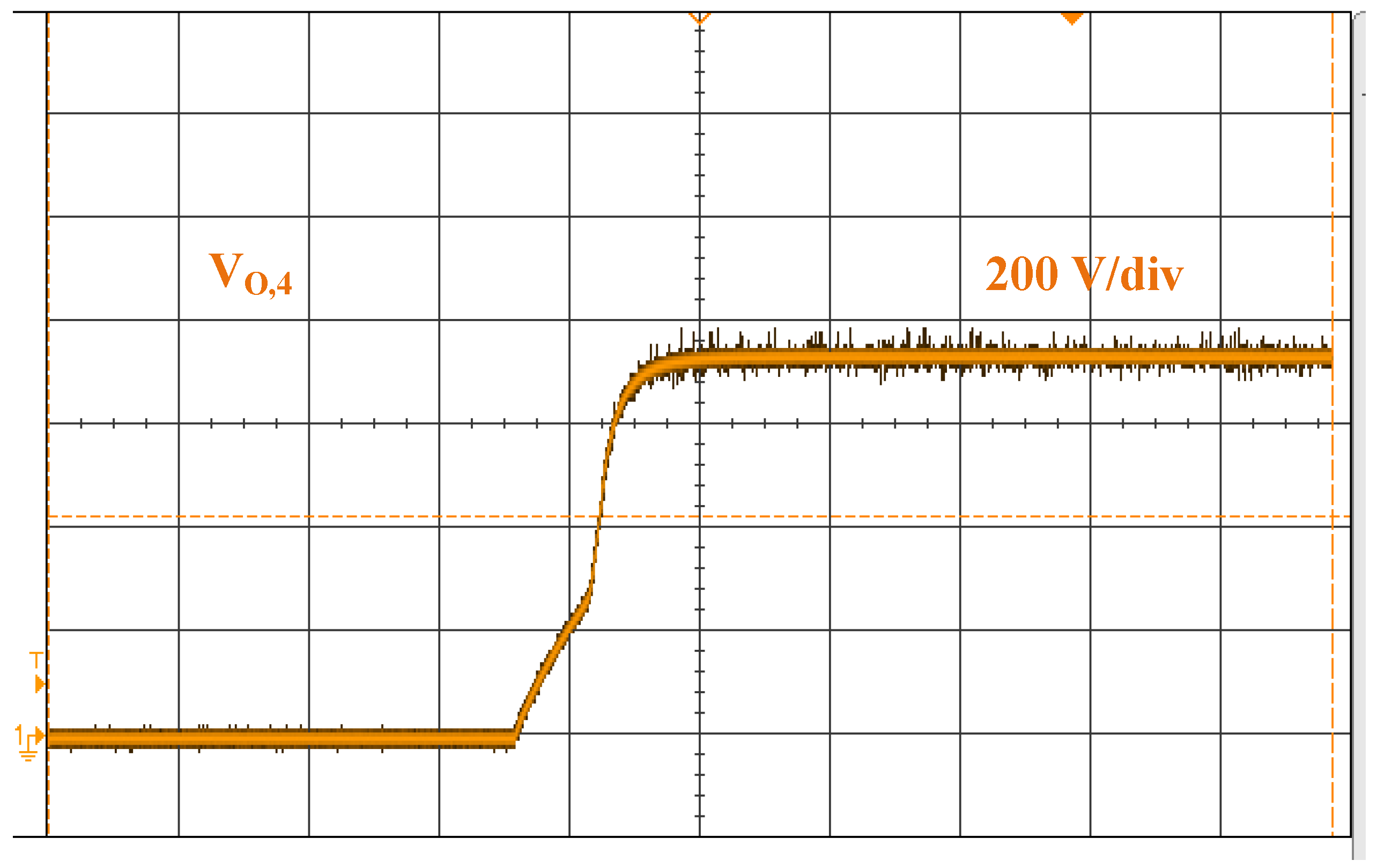
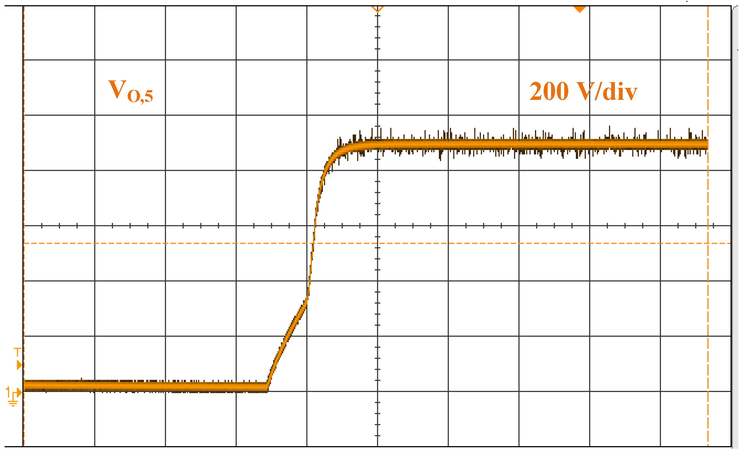
Figure 13,
Figure 14,
Figure 15 and
Figure 16, the voltage transients of all output stages during start-up are shown. There is no voltage spike detected on the output voltages in any of the stages; thus, the start-up of the converter is smooth. In
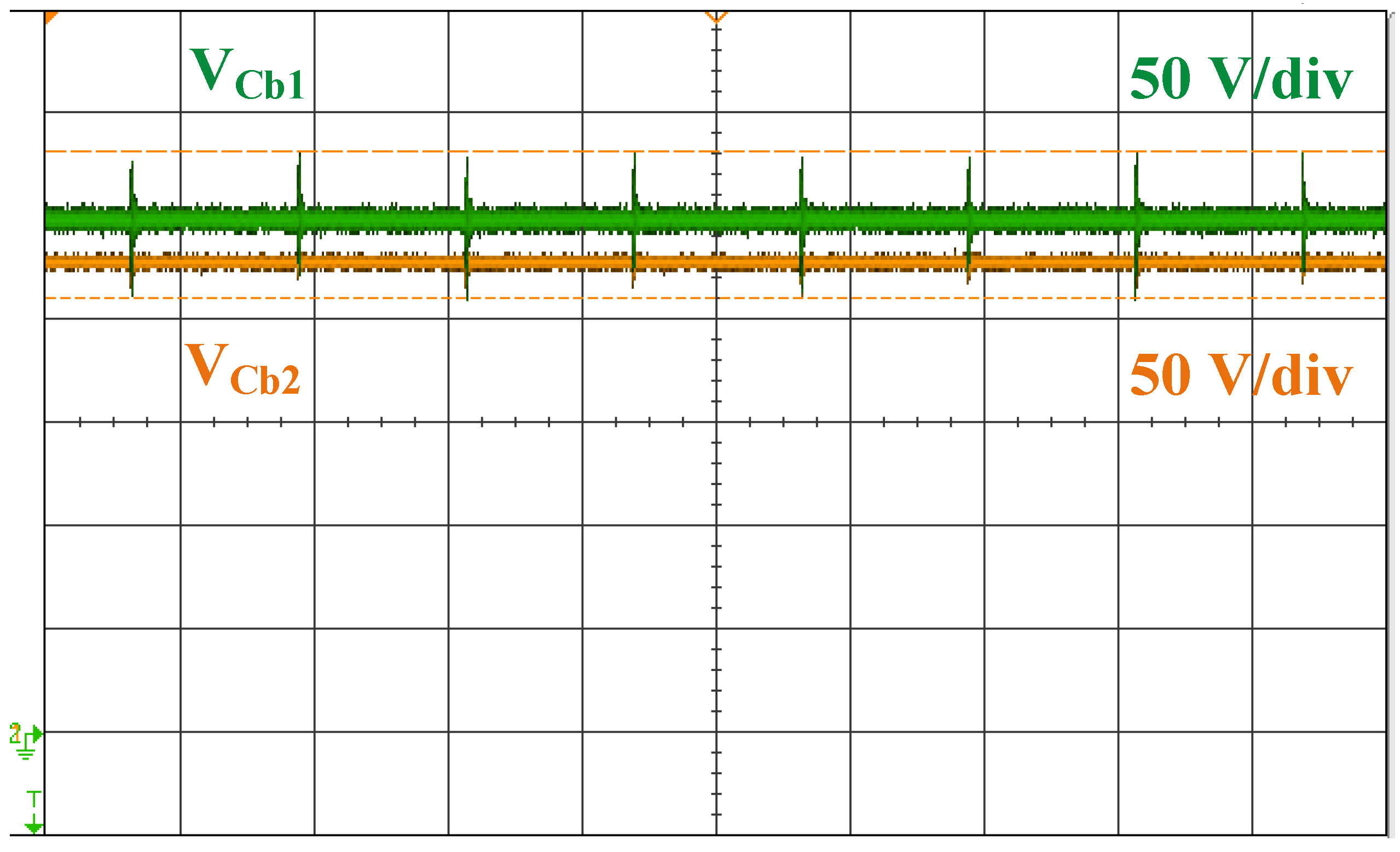
Figure 17 the unequal voltages of the input DC capacitors of the Half-Bridge are depicted, as was expected from the simulation results (
Figure 6b). In
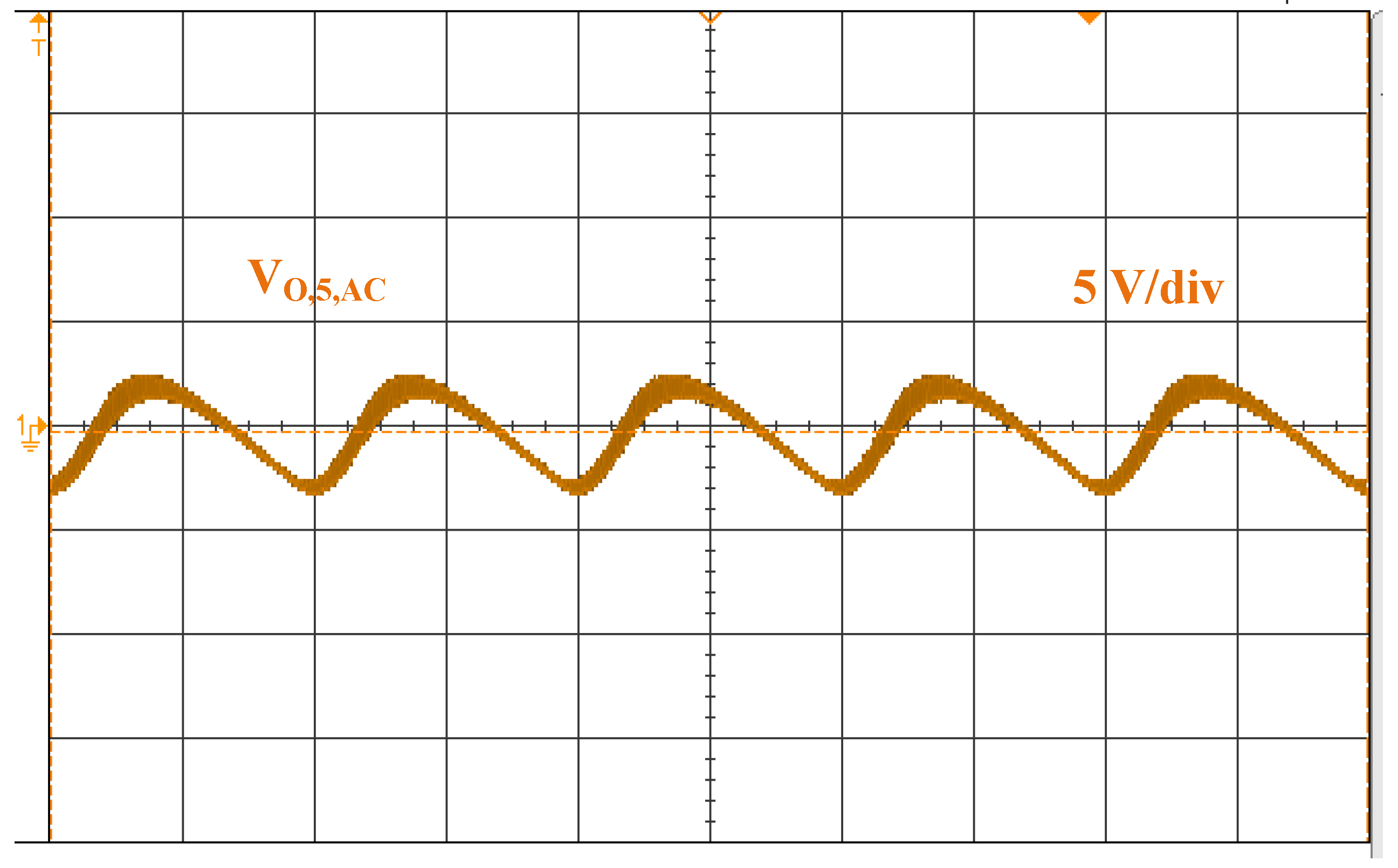
Figure 18, a ripple voltage of 0.3% for the maximum output level is shown, which is more than acceptable in our application.
Later, the consumption of the power converter was measured for different operating modes and the results are shown in
Table 3. For these measurements, a 1 MΩ resistor was connected to the output, in order to emulate the leakage of electrons in case of the PV panel regeneration.
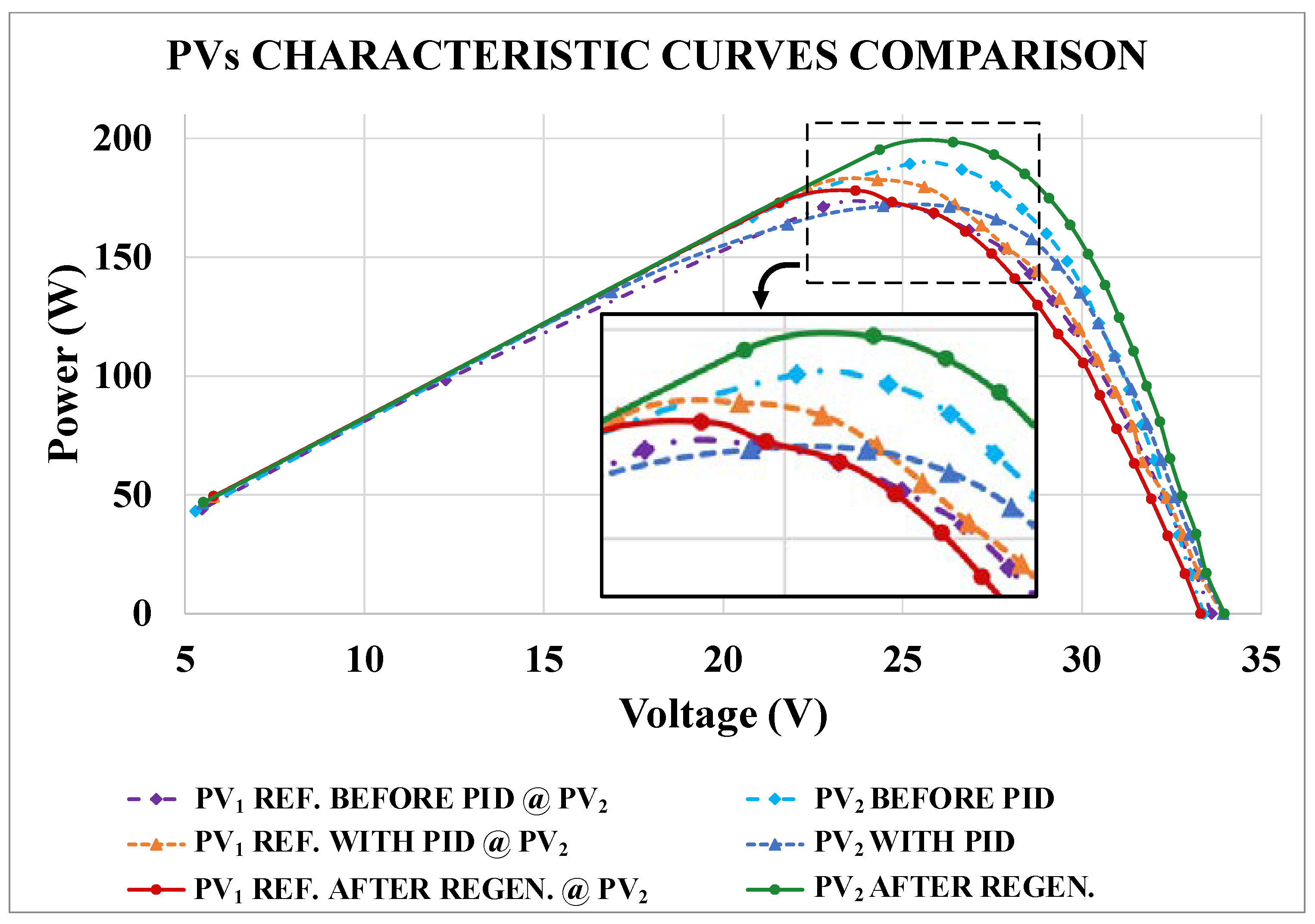
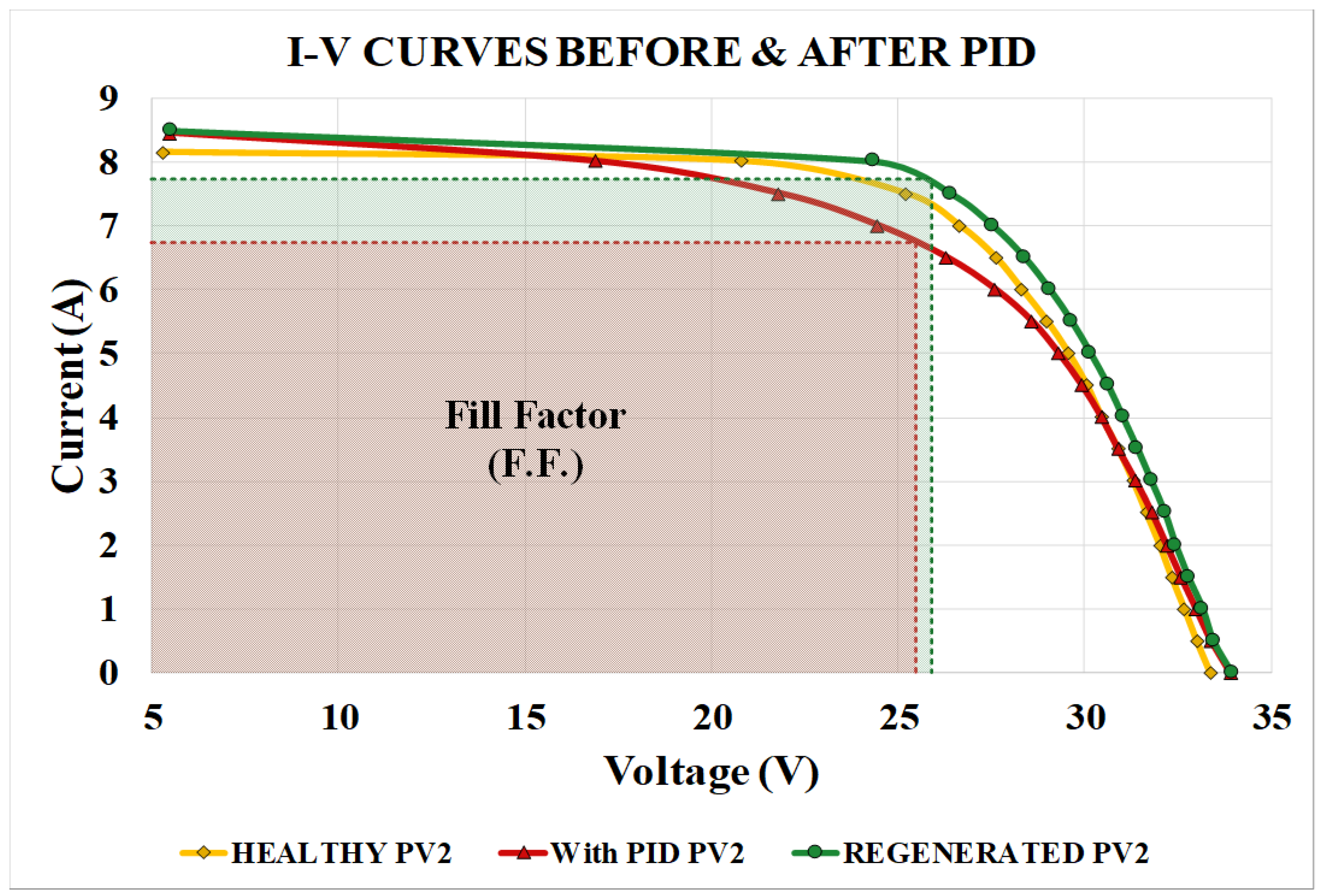
Afterwards, measurements on real PV panels followed, to verify the operational principles of the power converter, both for PID creation and regeneration of PV cells. First, the characteristic curves (P-V and I-V) of two PV panels (PV
1 and PV
2) were measured for several days at peak hours of solar radiation. The day with the group of data closest to the nominal ratings was selected. The corresponding curves are shown with dot-dashed lines in
Figure 19 and
Figure 20. Next, the proposed device is used to artificially create the PID phenomenon on PV
2. Reverse polarity was applied continuously for two weeks and then new measurements of the characteristic curves were taken for both panels. The P-V and I-V curves for this case are depicted with dashed lines. Afterwards, right polarity was applied to the PV
2 panel, in order to regenerate the PV cells and restore its power production capability. The curves after the regeneration process are depicted with continuous lines in
Figure 19 and
Figure 20.
By observing the curves in
Figure 19 and
Figure 20, important conclusions can be derived. Considering only the results of the panel under test PV
2, it is evident that after the enforced PID degradation, the output power generated by the PV is decreased, while after regeneration it is increased even beyond the initial state. However, the results could be ambiguous, since it is impossible for the solar radiation factor to be constant for all the tests. This is the reason why the PV
1 was used as the “control panel”, to have an indication of the solar radiation.
Before degrading the PV2, its power production was higher than PV1, as expected based on their nominal characteristics. After the PID emulation, the P-I and V-I curves of PV2 were measured lower than before, but the PV1 power production was increased, meaning that there was more solar radiation during those measurements. Therefore, it is absolutely verified that the PID was artificially created in PV2, by polarizing the panel with the proposed power converter.
After regenerating the PV2, its power production was increased with respect to the previous measurement where it was under PID. Meanwhile, the PV1 was measured lower than previously. Hence, the successful regeneration of the degraded PV cells is ensured, because a higher power and larger fill factor (F.F.) was detected compared to the previous case, even with lower solar radiation.
The experimental results at the MPP are shown in
Table 4 for the three different states of measurements: the initial healthy state, after enforced PID on PV
2 and after regenerating the PV
2 panel.


